Hierarchically assembled microspheres consisting of nanosheets of highly exposed (001)-facets TiO2 for dye-sensitized solar cells†
Abstract
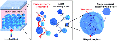
In this work, the mono-dispersed TiO2 microspheres with highly exposed (001)-facets (ca. 82%), high surface area (112.2 m2 g−1), and self-ordered 3D porous network have been rapidly synthesized by an in situ facet-controlling approach without any organic templates and employed as photoanodes of dye-sensitized solar cells (DSSCs). Owing to the stacking of 3D nanosheets of microspheres, the self-ordered internal porous network (ca. 30 nm) provides an efficient pathway for electrolyte and dye molecules penetrating into the interior part of a microsphere. Besides, the large voids among microspheres (ca. 300 nm) establish a highway for electrolyte diffusion. The formation processes of the prepared microspheres have been discussed, in which oriented self-assembly is involved. A reasonable mechanism is proposed to explain its high dye loading capacity (dye loading per gram/surface area of TiO2). Furthermore, according to the difference of normalized photocurrents of the cells with (001)-facet TiO2 and Ref-TiO2, the long wavelength region (600 to 800 nm) contributes 67.5% of the integrated photocurrent density; this result confirms its superior light scattering property. Finally, under 100 mW cm−2 light irradiation, a high photoelectric conversion efficiency of about 11.13% was achieved, as compared to that of the cell with a Ref-TiO2 film (8.11%). In light of their successful application in high-performing I3−/I−-based DSSCs, it is envisaged that these TiO2 microspheres with highly exposed (001)-facets can be used as excellent semiconductor materials in mass transfer limited cobalt-based DSSCs, and also in other fields, such as photocatalysis, water splitting, and lithium ion battery.
 Please wait while we load your content...

