I. Castro-Hurtado*ab,
J. Gonzalez-Chávarriab,
S. Morandic,
J. Samàd,
A. Romano-Rodríguezd,
E. Castañoab and
G. G. Mandayoab
aCeit-IK4 and Tecnun, Paseo Manuel Lardizabal 15, 20018, San Sebastián, Spain. E-mail: ichurtado@ceit.es; Fax: +34 943213076; Tel: +34 943212800
bCIC microGUNE, Goiru Kalea 9, Polo Innovación Garaia, Mondragón, Spain
cDipartamento di Chimica and NIS Inter-departamental center, Università di Torino, Via P. Giuria 7, 10125 Torino, Italy
dUniversitat de Barcelona (UB), MIND-IN2UB-Dept. Electrònica, C/Martí I Franquès 1, 08028 Barcelona, Spain
First published on 9th February 2016
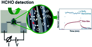
Tin dioxide nanowires have been grown by thermal oxidation of sputtered thin films by means of a VLS method. A tin sputtered layer catalyzed by gold nanoparticles acts as a material seed for the localized growth of NWs directly on gas sensor devices, avoiding the manipulation and transport of the nanowires to the electrodes. XRD and HRTEM analysis show that the nanowires crystallize in a rutile structure with a [100] preferential growth direction, and are single-crystalline with diameters lower than 50 nm. The response of nanowires to formaldehyde has been compared to thin film based sensors. A sensitivity of 0.10 ppm−1 is reported, twofold the sensitivity of the thin film, and short response and recovery times are measured (6 times shorter than thin films). The sensing mechanism proposed for the SnO2 NWs under formaldehyde exposure is explained by means of conduction measurements and FT-IR analysis. Oxygen species chemisorbed on the surface of each SnO2 nanowire produce a band bending, which generates a potential barrier (of 0.74 ± 0.02 eV at 300 °C) between the point contact of different nanowires. As evidenced by IR spectroscopy at 300 °C, electrons in the conduction band and in mono-ionized oxygen vacancies (at 0.33 eV below the bottom of the conduction band) are responsible for gas detection.
Among all the VOCs, formaldehyde (HCHO) is actually considered one of the first priority indoor air pollutants as described in the INDEX project.15 A significant source of formaldehyde in buildings are adhesives, plastics or pressed-wood products containing formaldehyde resins.16 Exposure to formaldehyde can cause nasopharyngeal cancer and pulmonary damage even at levels of 6 ppm.17 As a consequence, the Occupational and Safety Health Administration (OSHA) established a short-term exposure limit of 2 ppm and the National Institute for Occupational Safety and Health (NIOSH) states a long-term (30 min) exposure limit of 0.07 ppm.17,18 Thus, taking into account these detection standards, a fast and high sensitive HCHO sensor is required. The lack of commercial sensors that fulfil these requirements (high sensitivity, selectivity, stability and fast response), turns research on formaldehyde gas sensors necessary. It is worth noting that only very recent studies are targeted on HCHO detection by nanomaterials based sensors.4,5,19–24 Then, the need for development of an efficient and high sensitive HCHO sensor in a simple and cost-effective way is still present.
In this work, tin dioxide (SnO2) is selected as sensing material because most of the fundamental work done to explain the sensing mechanism of MOx gas sensors is developed based on the experimental results obtained with this n-type semiconductor as thick or thin film. In this way, a novel method to grow localized nanowires based on thermal oxidation of sputtered thin films is described. The precursor, the catalyst and the final nanowires are in the same spot. Thus, the NWs are grown on-chip and evenly distributed over the electrodes. Then, formaldehyde detection mechanism is studied in detail, focused on the elucidation of the effect of morphology of the sensing material. With this aim, characterization of the crystallinity and morphology of SnO2 nanowires and thin films is reported and their sensing characteristics are compared. The method proposed is suitable for growing high sensitive formaldehyde SnO2 NWs-based gas sensors by sputtering techniques, providing reliable response and mass production capability.
Absorption IR spectra were carried out on a Perkin-Elmer FT-IR System 2000 spectrophotometer equipped with a Hg–Cd-Tecryo-detector, working in the range of wavenumbers 7200–580 cm−1 at a resolution of 2 cm−1. The sample was placed in a commercial heated stainless steel cell (Aabspec) allowing thermal treatments in situ under vacuum or controlled atmosphere and the simultaneous registration of spectra at temperatures up to 600 °C.
![]() | ||
Fig. 1 Nanowire growing process by an annealing treatment of sputtered films at 900 °C and oxygen concentration of 6% over Pt electrodes on alumina substrate. |
Different factors can affect the growing process of the NWs, among them oxygen concentration is the most relevant parameter. Fig. 2a is a micrograph of the SnO2 nanowires grown on alumina substrate at 900 °C and under a 6% of oxygen concentration. An EDS element analysis of the NW sample shows a composition of Sn (67.51 wt%), O (30.63 wt%) and Al (1.87 wt%). If oxygen is not introduced during the annealing process (0% of O2), the Au–Sn liquid alloy particles solidify when the temperature is decreased. As a consequence, Au–Sn particles with diameters in the range of microns are obtained (Fig. 2b) with an element composition of Au (41.22 wt%), Sn (54.19 wt%) and C (4.59 wt%). In this case C comes from the carbon layer employed to cover non-conducting samples for SEM analysis. On the other hand, if oxygen is introduced in very high concentration (50% of O2), the oxidation of the Sn film is produced hampering the diffusion of the Sn atoms to the liquid alloy and avoiding the growth of the nanowires (Fig. 2c). The element composition is Sn (57.54 wt%), O (40.89 Wt%) and Al (1.47 Wt%) and the % Sn/% O ratio is diminished compared to the NWs. This confirms that fully oxidized big SnO2 clusters are obtained. Fig. 2d corresponds to the surface of a 200 nm-thick SnO2 thin film deposited by reactive sputtering. It serves to compare the different morphology that can be achieved by only varying the sputtering and thermal annealing process.
![]() | ||
Fig. 2 (a) SEM micrograph of samples grown at 900 °C and different oxygen concentrations. (a) 6% of O2. (b) 100% of N2 (c) 50% of O2, (d) SnO2 thin film deposited by reactive sputtering. |
The NW growing method can be easily transferred to the fabrication process of a gas sensing device, because only sputtering and annealing treatments are needed. Moreover it allows delimiting the sensing area (where the nanowires grow) by means of a photolithographic process. However, if the Pt–Sn phase diagram is examined,26 it seems that both Pt and Sn could be in a liquid phase at temperatures higher than 770 °C. In order to avoid a possible damage of Pt electrodes, a SnO2 protective layer was introduced before the Sn film deposition. A reactive sputtering in a mixture atmosphere of O2 and Ar was carried out to deposit a 50 nm thick SnO2 layer. Then, the oxygen was removed to continue with the deposition of the 1 μm-thick Sn layer over the SnO2 film and finally the 5 nm-thick gold film was deposited. Thus, only the tin film and gold nanoparticles would be melted and oxidized during the annealing process protecting electrodes and assuring good electrical contact. An image of the sample used for the testing measurement is shown in Fig. 3a and a cross section of the sensing device where Pt layer can be distinguished, showing a continuous and densely-packed film without defects is presented in Fig. 3b. Profiles of the elements across the EDS line-scan analysis of the cross section show a well-defined peak corresponding to platinum. It means that the Pt electrodes (200 nm-thick) are not affected by the high temperature annealing process. Moreover, the microstructure of nanowires is not affected by the addition of this SnO2 thin film as shown in the ESI (Fig. S3†), where micrographs of the SnO2 NWs grown on a chip over the Pt electrodes at 900 °C under 6% of O2 for 2 hours are shown.
![]() | ||
Fig. 3 (a) Image of the gas sensing device showing the SnO2 NWs over the electrodes and (b) FIB cross-section of the SnO2 NWs over Pt electrodes and EDS line scan analysis of the cross-section. |
Thus, this method provides an easy to implement technique suitable for mass production of gas sensing devices. As for example, with our sputtering equipment, 4 wafers of 3′′ × 3′′ dimensions have been processed at one time. Each wafer consists of 144 chips with dimensions of 6.35 × 6.35 mm. Thus, with one synthesis process 576 chips were obtained. As the uniformity in the Sn thickness layer is high (thicknesses of 1 μm ± 7% are measured), the concentration and length of the NWs is maintained.
The obtained NWs have been characterized by transmission electron microscopy (TEM). In Fig. 4a, conventional TEM analysis show the morphology of the samples, where some branching and kinking inside the nanowires can be observed. The NWs present different lengths and uniform widths ranging from 30 to 50 nm. In Fig. 4b, high-resolution TEM (HRTEM) images allow to confirm that the nanowires are single crystals, showing clear lattice fringes. Fast Fourier Transformation (FFT) of selected areas in the nanowires show interplanar distances of 4.74 Å, that correspond to (100) and (010) planes, in agreement with the a and b lattice constants of the rutile SnO2 (P42/mnm 136). Thus, the diffraction pattern can be indexed according to the tetragonal rutile SnO2 structure (PDF card 41-1145). The analysis indicates that the main growth direction of the nanowires is along [100] direction, in agreement with other studies on the VLS growth of the SnO2 nanowires.27
![]() | ||
Fig. 4 (a) TEM analysis of the SnO2 NWs (b) HRTEM images observed along (001) zone axis. The FFT of the area marked with dotted square is shown as inset. |
HCHO + O(ads)− → HCOOH + e− | (1) |
HCHO + 2O(ads)2− → CO2 + H2O + 4e− | (2) |
Sensor response is measured as the ratio of resistance of the sensing material in air and the resistance under the gas to be detected (SR = R0/Rgas).
In Fig. 5a the sensor response of the samples under 10 ppm of HCHO is presented at different operating temperatures. The maximum response (SR = 2.45) is obtained for a temperature of 270 °C. At this temperature, response and recovery times are 1.5 and 2.5 minutes respectively, which are within the time range expected by legislation. A faster response would be expected if the volume of the chamber (63 cm3) was decreased. Fig. 5b shows the transient response under different concentrations of HCHO at the operating temperature of 270 °C. The sensitivity of the sensor, change on sensor response per gas concentration unit (S = ΔSR/Δppm), calculated from the slope of the calibration graph is 0.107 ppm−1.23 The theoretical limit of detection (LOD) calculated from 3σ/b where σ is the standard deviation of the blank (baseline, response in air) and b the sensitivity, gives a value of LOD: 0.16 ppm assuming a linear range at low concentrations.
![]() | ||
Fig. 5 (a) Sensor response at different operating temperatures in dry air. (b) Comparison of dynamic response in dry air at 270 °C in a range of 2–20 ppm of SnO2 nanowires and thin film based sensor. |
In order to evaluate the advantages of the in situ grown SnO2 NWs with respect to conventional sputtered films, a sensing device based on a 200 nm-thick SnO2 film was also tested. A decrease in sensitivity and slower response than in NWs based sensors is obtained, which can be related to the compact morphology of the layer (average grain size of 30 nm). This result puts in evidence that the morphology of the sensing material plays a crucial role on formaldehyde detection. Fig. 6a shows the stability and repeatability of the sensor response tested at 270 °C under 5 ppm of HCHO in dry air. A small deviation from the baseline is measured, and the same experiment was repeated once a day during 5 days, resulting in a good stability with a 4% maximum variation. Moreover, the effect of humidity has to be considered when developing sensors for real environment applications. Fig. 6b shows the sensor response where the relative humidity (RH) has been varied in the range 0–80%. A decrease from 2 to 1.42 is measured when RH is raised to normal humidity conditions (40% RH). The interaction of water vapour at temperatures above 200 °C leads to the adsorption of hydroxyl groups. The bonding of these species increases surface conductivity in SnO2 films which is explained by the following reaction (eqn (3)).29
H2O + O(ads)− + 2Sn ↔ 2(Sn–OH) + e− | (3) |
![]() | ||
Fig. 6 (a) Repeatability measurements under 5 ppm at 270 °C and (b) influence of relative humidity on the sensor response of SnO2 NWs sensors. |
Hence, a competitive reaction is produced between vapour molecules and HCHO molecules. This causes the decrease in sensor response, because less reactive sites are available for HCHO molecules. Furthermore, selectivity against CO2, C6H6 and NH3 has been measured because they are within the major indoor contaminants.15 The PEL values as reported by OSHA are 1 ppm, 5000 ppm and 50 ppm for CO2, C6H6 and NH3 respectively.30 In this work, the response of the prototype to representative concentrations, above their indoor limits, have been selected on purpose. A good cross sensitivity (Q = SRHCHO/SRinterferent) of Q = 1.90, 1.92 and 1.95 against NH3, C6H6 and CO2 respectively is obtained compared to 5 ppm of HCHO (ESI Fig. S4†). In order to extend selectivity to other ubiquitous gases like ethanol or acetone, SnO2 NWs could be doped with NiO. It has been reported in other works that in both NiO–SnO2 films and nanowires a good selectivity against toluene, ethanol and acetone is obtained.11,31
With the aim of obtaining a general correlation between gas response and SnO2 morphology, Table 1 has been included to compare HCHO gas sensing characteristics of different works. It is clear that surface-to-volume ratio and porosity of the sensing material have impact on the sensing response and kinetics. Porous sensing layers based on nanofibers11,21 have a higher response than nanoparticle based compact films.31–33 This general assumption is consistent with the results from Xu et al.,24 where a sensitivity of 0.58 ppm−1 is measured for SnO2 micro-rods containing meso/macro-pores and decreases to 0.27 ppm−1 for thick films consisting in densely packed grains without pores.
Material form | Deposition technique | Operating temperature (°C) | Sensitivity (ppm−1) | Response time (min) | Recovery time (min) | Ref. |
---|---|---|---|---|---|---|
SnO2 NWs | Thermal oxidation PVD | 270 | 0.10 | 1.5 | 2.5 | This work |
SnO2 nanoparticle compact film | PVD | 270 | 0.055 | 8.5 | 14.5 | This work |
NiO-doped SnO2 NFibers | Electrospinning | 200 | 0.15 | 0.9 | 1.3 | 11 |
SnO2/In2O3 NFibers | Electrospinning | 375 | 0.285 | 2 | 2 | 21 |
SnO2 hierarchical porous micro-rods | Screen printing | 320 | 0.58 | 0.07a | 0.33a | 24 |
SnO2–NiO nanoparticle compact film | Co-precipitation | 300 | 0.055 | 0.3 | 1 | 31 |
Pd-doped SnO2 nanoparticle compact film | Sol–gel | 250 | 0.04 | 2b | 1b | 32 |
Cu-doped SnO2 nanoparticle compact film | Co-precipitation | 200 | 0.010 | 3.5 | 3 | 33 |
Our samples attend to the same principle, as single-crystalline NW array shows better sensing characteristics than polycrystalline compact thin films. These results are in accordance with the gas diffusion/consumption model developed by Iizuka et al. for HCHO detection with SnO2 porous films.34 In that work, both theoretical and experimental results predict a higher sensor response for films containing micro- and macro-pores than those including only micro-pores. With respect to the response kinetics, the discussion might be focused on studies that test samples with different morphologies but under the same conditions such as volume chamber, gas flow and operating temperature. In the work from Xu et al.24 response time increases from 4.3 seconds in SnO2 micro-rods to more than 1 minute for densely packed thick films. They suggest that, for a given temperature and in the absence of a catalyst that promotes surface reaction, gas diffusion should be considered the first factor controlling the rate of response. In this way, single-crystalline NW array presents numerous channels for gas transport whereas SnO2 thin film restricts gas transport to inner particles due to particle agglomeration.
O2(ads) + e− ↔ O2(ads)− | (4) |
O2(ads)− + e− ↔ 2O(ads)− | (5) |
O(ads)− + e− ↔ O(ads)2− | (6) |
Electron transfer from conduction band to chemisorbed species gives rise to a negatively charged surface region. In order to preserve electrical neutrality, a positive space charge layer of width w, also called depletion region, is developed in the surface. This causes a shift in the electrostatic potential and an upward bending (qVs) of the energy bands toward the surface.38 This upward bending generates a potential barrier between point contacts (primarily grain boundaries) that electrons have to overcome during conduction. Thus, the conductance of the sensing material is dependent on the potential barrier and the following relationship serves as a link between surface states (chemisorbed oxygen species) and measured conductance.39
![]() | (7) |
In the case of SnO2 NWs this barrier model can be applied to the electron transport between neighboring nanowires, as there is a point contact between them and the thin layer, which assures percolation and barrier crossing. Thus, the conductivity of the nanomaterial is exponentially dependent on the potential barrier which is related to the activation energy of conduction on changing temperature.40 In order to evaluate the height of the potential barrier, temperature-stimulated conductance measurements have been carried out. This method, explained in detail in the work from Carotta et al.,41 consists in evaluating the conductance transient response under a fast temperature change. This data is shown in Fig. S5 in the ESI.† Fig. 7 shows the dependence with temperature of the barrier energy measured for SnO2 NWs in air. Above a transition temperature of 200 °C, also observed in screen printed SnO2 thick films,41 the value of the barrier energy increases up to 0.74 ± 0.02 eV at 300 °C. This means that the amount of adsorbed oxygen species is greater above this temperature and as a consequence the sensor response of the material to reducing gases like HCHO might increase. Similar values in the range 0.55–0.7 eV are reported by Malagù et al.,42 calculated with the same method for SnO2 nanoparticles (>30 nm) obtained via sol–gel route. Moreover, a value of 0.6 ± 0.1 eV is estimated by Kwoka et al.43 by photoemission studies of non-stoichiometric ([O]/[Sn] = 1.20) L-CVD deposited SnO2 films, whereas samples close to stoichiometry ([O]/[Sn] = 1.95) correspond to near flat band conditions.
![]() | ||
Fig. 7 Energy barrier dependence on temperature in dry air of the SnO2 NWs calculated by stimulated temperature conductance changes. |
Furthermore, to gain deeper insight into the role of oxygen vacancies and chemisorbed oxygen species, FT-IR studies of the sensing material have been performed. It allows following the electrical absorption variations induced by gaseous environment change. In this way, it is possible to put in evidence the injection of electrons in the material during the interaction with formaldehyde. For this analysis, SnO2 NWs have been grown on silicon substrate that allows spectra recording in transmission mode. The synthesis process is the same followed for the device fabrication on alumina substrate and the same microstructural properties are obtained. The sample is preventively treated at 550 °C in dry oxygen to let oxygen species adsorb on the surface of the semiconductor following eqn (4)–(6). Then, the interaction with 20 mbar of pure formaldehyde at temperatures in the range 100–350 °C with increasing steps of 50 °C is studied. In this second stage, reactions of HCHO with adsorbed species are produced as described in eqn (1) and (2). It is important to point out that FT-IR spectra are reported as difference spectra, where the subtrahend spectrum is always that of the oxidised sample (after treatment at 550 °C) recorded in O2 at the same temperature as in formaldehyde. Examples of the spectra in O2 and in HCHO are shown in the ESI (Fig. S6†). This operation allows putting in evidence sample modification induced by formaldehyde interaction and allows avoiding baseline changes arising from temperature increase.
In Fig. 8 difference spectra of SnO2 nanowires after interaction with formaldehyde at increasing temperature are reported. Up to 250 °C, no modifications induced by formaldehyde are observed. Only roto-vibrational modes of formaldehyde in the gas phase are evidenced. Starting from 300 °C, very broad absorption, extended from 1000 to 5000 cm−1 starts to develop and increases in intensity on increasing temperature. This broad absorption is centered at about 2700 cm−1 which corresponds to energy of 0.33 eV. As known, oxygen vacancies are the predominant intrinsic defects in SnO2 crystals and powders in the range of temperatures in which our samples have been prepared.44 Thus, this absorption is related to the electronic transition from the energy level of oxygen vacancies to the conduction band. It can be assigned as the second ionization energy of oxygen vacancies, which in traditional nano-structured SnO2 powder appears at 1200 cm−1 (at a lower energy of 0.15 eV).38,44 First ionization energy of oxygen vacancies (0.03 eV) allows the thermal excitation of electrons in the conduction band already at room temperature and it is not detectable in the medium IR region.
![]() | ||
Fig. 8 FT-IR difference spectra of SnO2 NWs in interaction with 20 mbar of HCHO at 250 °C (black line), 300 °C (red line) and 350 °C (blue line). |
In accordance with the obtained results, a model of the sensing mechanism for the in situ grown SnO2 NWs is proposed. Oxygen adsorption is produced by two different paths: one involves conduction band electrons, which influences band bending and electrical conductivity, and the second, evidenced in the FT-IR analysis, is associated to electrons trapped in mono-ionized oxygen vacancies. Regarding the first path, morphology of the nanowires is decisive because electron conduction is limited by the presence of potential barriers between point contacts. Henceforth, in the case of our single-crystal SnO2 NWs, as they are free of grain boundaries, each nanowire acts as a conduction channel where electrons move freely. The very thin layer (50 nm) deposited over the Pt electrodes serves as a buffer layer that puts into contact different nanowires and drives the electrons to the electrode.45 These electrons must overcome a potential barrier generated in the point contacts of adjacent NWs or passing through the NW to the buffer layer as shown in Fig. 9a. The height of this potential barrier depends on temperature, as it is related to oxygen ionosorption mechanism which gives rise to gas detection. A good ohmic contact between sensing material and Pt electrodes is verified by I–V curves of the samples (ESI Fig. S7†) measured in two probe mode. A linear behaviour with the applied voltage (−5 to +5 V) throughout the entire temperature range (200–300 °C) is obtained.46
On the other hand, Fig. 9b shows the energy band diagram of the n-type semiconductor considering two paths for oxygen ionosorption. As revealed in the FT-IR analysis, a transfer of electrons from mono-ionized oxygen vacancies to oxygen species is produced, generating bi-ionized oxygen vacancies
. This is described in the band diagram by the formation of new donor levels below the conduction band (Ed2). During the interaction with formaldehyde (Fig. 9c), HCHO molecules react with adsorbed oxygen species (eqn (1) and (2)), and electrons are released. These electrons replenish the conduction band and the potential barrier decreases (from qVs1 to qVs2) giving rise to a smaller depletion region w2 < w1 (Fig. 9c). As evidenced in IR spectra, electrons also re-populate oxygen vacancies in a significant way at 300 °C. Thus, bi-ionized oxygen vacancies
are populated by the released electrons and mono-ionized oxygen vacancies
are created. In this way, the broad absorption centered at 2700 cm−1 can be related to the photo-ionization of
by the incident IR radiation
. This broad absorption in the difference spectra validates the fact that HCHO re-populates
creating new
for photo-ionization, otherwise the spectra in O2 and in HCHO would be the same.
The NWs based sensing devices have been tested under HCHO concentrations in the range 2–20 ppm. Moreover, their sensing characteristics have been compared to SnO2 thin films gas sensors, to put in evidence the influence of morphology on the detection mechanism of HCHO. Nanowires present higher sensitivity at the operating temperature of 270 °C and shorter response and recovery times.
A sensing mechanism is proposed for these in situ grown SnO2 NWs, which stablishes a relation between conductance and surface states (oxygen chemisorbed species). Oxygen species are adsorbed as they pick-up electrons from the conduction band generating a potential barrier, that increases above 200 °C. On the other hand, at 300 °C also mono-ionized oxygen vacancies play a role on oxygen adsorption. At this temperature, HCHO interacts with chemisorbed oxygen species in a significant way, re-populating bi-ionized oxygen vacancies and replenishing the conduction band. This result may explain the high response of the nanowires at 270 °C. This work opens up a new window for the development of reliable and low cost nanomaterials based gas sensors.
Footnote |
† Electronic supplementary information (ESI) available. See DOI: 10.1039/c5ra26105h |
This journal is © The Royal Society of Chemistry 2016 |