Qayyum Zafar*a,
Fakhra Azizab and
Khaulah Sulaimana
aLow Dimensional Materials Research Centre (LDMRC), Department of Physics, Faculty of Science, University of Malaya, 50603 Kuala Lumpur, Malaysia. E-mail: qayyumzafar@gmail.com; Fax: +60 3 79674146; Tel: +60 1 73738342
bDepartment of Electronics, Jinnah College for Women, University of Peshawar, Peshawar 25120, Pakistan
First published on 26th January 2016
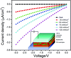
Herein, we demonstrate a novel solution-processed photodetector using an organic composite blend of VOPcPhO and PCDTBT to function as the donor (D) and the acceptor (A) materials, respectively. The absorption spectra of the composite blend have been successfully broadened to encompass almost the entire visible region by exploiting the spectral properties of PCDTBT moiety. The photodetector shows an efficient photo-current response as a function of varied illumination levels. Furthermore, current density–voltage (J–V) characteristics of the device, in the dark, have been employed to extract device parameters such as barrier height and rectification ratio. The conduction mechanisms at the electrode–semiconductor interface have also been investigated. As the proposed photodetector can harvest incident photons over almost the whole visible range, it can be potentially employed for practical applications.
In recent years, metal phthalocyanines have attracted much attention in photovoltaic applications owing to their high p-type conductivity, chemical and thermal stability.4–6 Phthalocyanine molecules are mostly conjugated i.e., they contain π–electron system,7 which is a key to their good photosensitivity.8 Among the metal phthalocyanine, vanadyl 2,9,16,23-tetraphenoxy-29H,31H-phthalocyanine (VOPcPhO) is capable to act as a sensitizer of photo-induced electron transfer when blended with a suitable acceptor material.9 VOPcPhO is a macro-cyclic compound consisting of four isoindole units surrounding the centre vanadyl metal atom.10 In our previous study,11 we reported that VOPcPhO exhibits intense light absorption in the visible wavelength range, thus making it suitable for photodetection application. However, since VOPcPhO is unable to absorb light in 450–600 nm range, therefore it needs to be blended with a suitable acceptor material (possessing complementary absorption spectra in lower energy wavelength range), so that it may lead to efficient light absorption in nearly whole visible spectrum.
Low bandgap co-polymers based on polycarbazole derivatives, exhibiting alternating donor acceptor moieties have also recently attracted significant attention. These copolymers have been developed with deeper highest occupied molecular orbital (HOMO) energy levels to harvest the incident photons in the low energy part of the solar spectrum. In general, these copolymers are characterized by the internal charge transfer from an electron-rich unit to an electron-deficient moiety within each repeating unit. Among these copolymers, poly[N-9′-heptadecanyl-2,7-carbazole-alt-5,5-(4′,7′-di-2-thienyl-2′,1′,3′-benzothiadiazole)] (PCDTBT) has been subjected to intense study for the fabrication of field effect transistors and solar cells. PCDTBT is a non-crystalline copolymer and is characterized by an intermediate level of order resulting from π–π stacking between the conjugated back-bones. Further the copolymer is stable towards oxidation from air as previously suggested by Y. S. Peng et al., since the HOMO energy level of PCDTBT (5.45 eV) is well below oxidation threshold from air (5.27 eV).12
Albeit, PCDTBT donor–acceptor copolymer is believed to be a typical p-type material, but in the present work we have utilized it as an acceptor material. Prior to this study, S. Cho et al., have also reported n-type electron mobility as high as 5.8 × 10⁻⁴ cm2 V−1 s−1 in PCDTBT based ambipolar FET.13 Further, as previously reported by C. R. McNeill, that the assignment of donor and acceptor is relative and is determined by the relative position of HOMO and lowest unoccupied molecular orbital (LUMO) energy levels, so a polymer that acts as an electron donor in one combination may also work as an electron acceptor in another combination.14 K. Yao et al., also described that the same conjugated polymer can operate either as an electron-acceptor or an electron-donor provided that its energy levels have the correct offsets with respect to its counterpart in the blend.15 The present work is motivated by the polymer optoelectronic devices approach, in which n-type polymer is used as an acceptor material instead of fullerene derivatives.14–17 The unique advantage of this approach is broad absorption profile of photoactive layer owing to the synergetic or complementary absorption of donor and acceptor materials. The low bandgap polymers have high absorption coefficients in the low energy visible spectral region (red and near-infrared regions), while fullerene derivatives are typically unable to absorb low photon energies.16 Therefore, we find it interesting to investigate VOPcPhO as a donor and PCDTBT as an acceptor material by virtue of their complementary absorption profile.
Finally VOPcPhO and PCDTBT both are readily soluble in a common solvent (chloroform) and interact in a way to favor phase-separated domains. This favorable mixing property not only renders them suitable for solution processability but also facilitates the creation of nanoscale, phase-separated morphologies required for optimum device operation. In the present work, PCDTBT has been anomalously used as an acceptor and VOPcPhO as a donor to form a composite blend for a solution-processable visible wavelength photodetector. The spectral properties of both moieties have been exploited to broaden the absorption spectra of the composite blend which encompasses almost the entire visible region between 350 and 800 nm.
Indium tin oxide (ITO) coated glass substrates (25 × 25 mm dimension, sheet resistance ∼ 10 Ω sq−1), were cleaned by ultrasonic treatment in soap water, de-ionized (DI) water, acetone, isopropyl alcohol and DI water sequentially and were subsequently dried by nitrogen blow in a dust free environment. A 45 nm-thick PEDOT:PSS anodic buffer layer was spun cast onto the ITO substrates and dried at 120 °C for 30 min on a hot plate. However prior to the thin film deposition, PEDOT:PSS aqueous solution was filtered by commercially available nylon 0.45 μm filters to avoid any solid contents. PEDOT:PSS not only smoothes out the rough surface of ITO but also increases the anodic selectivity by increasing electron blocking.18
25 mg ml−1 concentrated solutions for both VOPcPhO and PCDTBT were prepared in chloroform separately and stirred overnight using a magnetic stirrer. The organic blend was then prepared by mixing VOPcPhO and PCDTBT solutions in five different stoichiometries by volume (2:
1, 1.5
:
1.0, 1
:
1, 1.0
:
1.5 and 1
:
2). The organic D/A binary blend with stoichiometry of interest, was later spin coated on the ITO/PEDOT:PSS substrates at a speed of 2500 rpm to achieve ∼100 nm thickness of photoactive thin film. Albeit, organic photoactive film is generally annealed, which not only causes recrystallization but also reduces the free volume and the density of defects at the interfaces.19 However, in the present study, annealing was avoided since it is known to have a deteriorating effect on the performance of PCDTBT based devices.20,21
Finally, to complete device fabrication process, lithium fluoride (LiF) and aluminium (Al) electrodes were deposited by thermal evaporation at high vacuum 3 × 10⁻⁵ Torr through a shadow mask with circular openings of 2 mm2. LiF is particularly used as a cathodic modification material to improve the performance of the organic photovoltaic (OPV) devices and organic photodetectors.22,23 In the present work LiF thin film (∼3 nm) has been deposited to form an effective interfacial dipole between Al and organic semiconductor, which results in lowering the work function of Al cathode as previously suggested by Y. S. Peng et al.12
All the fabrication process was conducted in open air inside the clean room. The cross-sectional view of the fabricated ITO/PEDOT:PSS/VOPcPhO:PCDTBT/LiF/Al OPD and energy level diagram of the components is shown in Fig. 2(a) and (b), respectively. As is well known that while selecting the photoactive material pair, their HOMO and LUMO energy levels should support the exciton dissociation at the D/A interface. If the energy offset of the LUMO and the HOMO between the donor and acceptor is large enough, excitons will be promptly dissociated into electron–hole pairs with a difference in binding energy near the donor/acceptor interface due to the preferable properties of charged carriers with regard to energy.24 The energy-level diagram of the OPD shows a good choice of organic VOPcPhO (D) and PCDTBT (A) materials, exhibiting sufficient offset for the efficient charge separation.25
![]() | ||
Fig. 2 (a) Schematic diagram of the ITO/PEDOT:PSS/VOPcPhO:PCDTBT/LiF/Al photodetector (b) schematic energy band diagram of the device components referenced to the vacuum level. |
In the present study, X-ray diffraction patterns (XRD) were obtained from the Panalytical Xpert pro. AFM images were obtained from Agilent Technologies 5500 atomic force microscope. UV-vis absorption spectra were carried out using a UV-vis-NIR spectrophotometer (Shimadzu UV-3101PC). The steady state photoluminescence (PL) characteristics were measured by RENISHAW inVia Raman microscope instrument. During PL measurements the laser source of 325 nm wavelength was used. The current density–voltage (J–V) characteristics of the fabricated photodetector were measured using computer interfaced Keithley source measuring unit (SMU) under varied illumination levels of AM1.5G-filtered irradiation from an Oriel 67005 solar simulator.
The morphology of solution-processed thin films of pristine VOPcPhO, PCDTBT and VOPCPhO:PCDTBT composite blend as prepared on glass substrates has been investigated by atomic force microscopy (AFM). Fig. 4(a)–(c), show distinguished 3D AFM micrographs of the pristine VOPcPhO, PCDTBT and their binary composite, respectively, along with their cross sectional profile obtained in tapping mode. It can be clearly observed from the figure that morphology of the thin film VOPcPhO exhibits quite rougher surface as compared to that of PCDTBT with rms roughnesses of both films equal to 7.33 and 3.81 nm, respectively. Based on the AFM cross section profiles of the thin films, the results indicate that increased surface contact area between VOPcPhO and PCDTBT may lead to larger interface area between the donor and acceptor of the composite blend thus benefiting the charge extraction in a polymer based photodetector.
![]() | ||
Fig. 4 3D AFM micrographs and cross sectional profiles of (a) VOPcPhO, (b) PCDTBT, (c) VOPcPhO:PCDTBT binary composite blend and (d) phase image of donor–acceptor (VOPcPhO:PCDTBT) blend. |
It is well known that in order to have a clearer view of charge separation and carrier transport, proper phase separation of donor and acceptor domains and their interpenetrating networks are needed. Numerous studies on the morphological investigation on the blended thin films employed in the bulk heterojunction solar cells suggest that optimal morphology for device operation is to have segregated domains.29,30 To study the domain segregation in our blend film, phase image of the VOPcPhO:PCDTBT blend has also been obtained and is presented in Fig. 4(d). The image reveals evidence of phase separation with two distinct domains. The dark and light brown phases correspond to donor-rich material and acceptor rich-material, respectively.31
Fig. 5 (inset) shows absorption spectra of pristine thin films of VOPcPhO and PCDTBT, independently. Absorption peaks of the donor material VOPcPhO are located at 350 nm (Soret band) and at 677 and 713 nm (Q band).11,32 The UV-vis spectrum of VOPcPhO thin film exhibits an extensive valley between 400 and 600 nm as previously reported.10 Since, PCDTBT shows its main absorption peaks over this valley, hence, merging these two materials together; a broader absorption spectrum can be realized. The donor–acceptor copolymer PCDTBT exhibits two distinct absorption bands in the visible region of the spectrum with their maxima lying near 400 and 560 nm. These two strong absorption bands are assigned to π–π* transitions into the first and second excited singlet state.33,34 Fig. 5, portrays the absorption spectra of VOPcPhO and PCDTBT binary blends in five different stoichiometries by volume (2:
1, 1.5
:
1.0, 1
:
1, 1.0
:
1.5 and 1
:
2). The broad absorption spectrum of the binary blend covering whole visible spectrum is by the virtue of the complementary absorption spectra of VOPcPhO and PCDTBT. It can be inferred from Fig. 5, that by increasing the loading ratio of VOPcPhO in PCDTBT:VOPcPhO binary blend; increased absorbance at large wavelength region is observed.
![]() | ||
Fig. 5 UV-vis absorption spectra of VOPcPhO, PCDTBT and their binary composite blend in five different volumetric ratios. (Inset) Absorption spectra of pristine thin films of VOPcPhO and PCDTBT. |
Steady state photoluminescence (PL) study of the VOPcPhO:PCDTBT composite has been conducted to investigate the efficiency of exciton dissociation. Fig. 6 (inset) presents PL measurements of the pristine VOPcPhO and PCDTBT, independently. Fig. 6, shows the PL spectra of VOPcPhO:
PCDTBT BHJ organic blend in five different volumetric ratios (2
:
1, 1.5
:
1.0, 1
:
1, 1.0
:
1.5 and 1
:
2), measured at room temperature in the wavelength range 400 to 1000 nm. It is quite evident that the VOPcPhO quenches the spectra due to the photoelectrons generated by the PCDTBT for λex 700 nm excitation. These results suggest that the photoinduced charge carriers in the photoactive blend can be efficiently separated through the phthalocyanine–copolymer interface. A prominent maximum PL quenching of PCDTBT emission has been observed at the optimal loading ratio of 1
:
0.6 (by volume) of the composite blend. The PL quenching suggests that the phase separation between VOPcPhO and PCDTBT matrix occurs within the exciton diffusion length scale for 1
:
0.6 stoichiometric composition. The quenching is assumed to arise due to the efficient non-radiative channel for charge transfer between the donor and acceptor phases.
![]() | ||
Fig. 6 Photoluminescence spectra of VOPcPhO and PCDTBT blends in various volumetric ratios. (Inset) PL spectra of VOPcPhO and PCDTBT, when studied independently. |
When the photodetector is exposed to illumination, incident photons with sufficient energy are absorbed by the photoactive layer and excitons are generated. These excitons are tightly bounded (usual binding energy ∼ few hundred meV), because of the low dielectric constant of organic materials.35 It is well-known that in an organic BHJ, donor and acceptor components are intimately blended with phase separation at nanoscale (usually 10–20 nm). Therefore, due to the existence of sufficient D/A interfaces in BHJ structure, excitons can easily reach to them and decay into charge transfer (CT) state, thereby, leading to domain-segregated electrons and holes.36 The dissociation process of excitons is driven by the significant offsets in LUMO energy levels of donor and acceptor materials.37 The free charge carriers created at the D/A interface are diffused and drifted to the corresponding electrodes, thus contributing to photocurrent in the external circuit.
As the basic photo-response of an organic photodetector,38,39 the reverse biased current density–voltage (J–V) characteristics at varied incident light intensities have been obtained and depicted in Fig. 7. When light impinges on the OPD, the generated electron–hole pairs are swept away by the built-in D/A energy level offset, resulting in photocurrent even at zero bias. It is evident from the Fig. 7, that the photocurrent of the VOPcPhO:PCDTBT composite blend is considerably enhanced with increasing light intensities. Under illuminated condition, excitons are generated in the photoactive blend, which diffuse into the PCDTBT:VOPcPhO junction and disintegrate due to the built-in electric field. The HOMO energy level of PCDTBT is lower than that of VOPcPhO, indicating that holes can be easily transported from PCDTBT to both VOPcPhO and PEDOT:PSS ultimately reaching ITO anode. The responsivity of the sensor has been determined as 23.5 μA W−1. The light to dark current density ratio (Jph to Jd) of the fabricated OPD at −3 V operational bias has been calculated to be ∼695.36.
![]() | ||
Fig. 7 Typical current density–voltage (J–V) characteristics of the ITO/PEDOT:PSS/VOPcPhO:PCDTBT/LiF/Al photodetector measured at various illumination intensities between 0 and 125 mW cm−2. |
Similar behaviour is revealed when the photocurrent density is measured under different operational biasing. Fig. 8, portrays that the sensitivity of the photodetector is significantly dependent upon the operational bias. The reverse biased photocurrent density–voltage characteristics exhibit a noticeable upsurge along the Y-axis under illumination. The higher sensitivity of the photodetector at higher order of operational bias may be attributed to two possible reasons; (1) enhanced charge generation due to the extended absorption bandwidth of the composite thin film, (2) external field assisted efficient charge transport towards the respective electrodes before recombination. In general, photocurrent can be expressed as a power function of light intensity, as explained by the following equation:40
Ilight = AFα | (1) |
![]() | ||
Fig. 8 Light intensity vs. current density for ITO/PEDOT:PSS/VOPcPhO:PCDTBT/LiF/Al photodetector at varied bias voltages. |
The forward and reverse biased semi-log I–V response of the diode is of vital importance as it provides information about junction parameters such as reverse rectification ratio ‘RR’, saturation current ‘IS’, ideality factor ‘n’, barrier height ‘Φb’. Fig. 9, depicts semi-log I–V response of ITO/PEDOT:PSS/VOPcPhO:PCDTBT/LiF/Al OPD measured in dark condition at room temperature. It can be seen that at reverse biasing, the rise in amplitude of the dark current is low as compared to the forward-biased current; such nonlinear and asymmetric response reveals that the fabricated device exhibits rectifying behavior. For the present case, the OPD has been observed to exhibit the RR ∼ 2 at ±3 V and reverse saturation current density (Js) has been measured as ∼0.7 nA cm−2. To analyze the photodiode characteristics quantitatively, we have assumed standard thermionic emission model of a Schottky junction. According to the aforementioned model, diode current equation in dark condition can be described by the Shockley equation.41
![]() | (2) |
![]() | (3) |
The slope of linear region of the forward bias lnI–V plot has been used to determine the ideality factor n for the device. Using eqn (4), value of n has been calculated as 3.31. Admittedly, the ideality factor is a measure of diode conformity and in general its value must be close to 1,43 but in most organic semiconductor based devices the value of ‘n’ is observed to be much greater than one.44,45 The deviation of ideality factor from unity may be attributed to several reasons such as barrier inhomogeneity, high interface state density, interface dipoles and generation–recombination and tunneling.46–48 From the y-intercept of the forward bias semi-log I–V response, the value of the barrier height (Φb) existing at the metal–semiconductor interface of the OPD has been estimated as 0.63 eV, using eqn (5). The value of Φb is in consistence with the values previously reported in literature.49,50
![]() | (4) |
![]() | (5) |
Generally, charge transport of thin film based organic devices can be divided into two categories i.e. charge injection at contacts and charge transport in the bulk.51–53 The analysis of the forward bias I–V curves, in the dark, can providing sufficient information about the transport mechanisms controlling the conduction process at the electrode interface of the device. In order to realize conduction mechanism which controls the device behaviour, I–V characteristics of ITO/PEDOT:PSS/VOPcPhO:PCDTBT/LiF/Al photodetector have been re-plotted on double logscale in Fig. 10. The double logarithmic forward bias I–V plot of Fig. 10 shows two distinct regions which obey power law (I ≈ Vm+1) behaviour of current with different exponents (m + 1). In region I, at lower voltages, the slope is nearly equal to ‘1’ which indicates ohmic region. The current is directly proportional to the applied voltage, in this region. At higher voltages in region II, the slope is measured as ∼2 which suggests that the dominant transport mechanism is space charge limited current (SCLC). In transition from ohmic to SCLC region, traps present in the active layer play a critical role.54 Since the traps in this region are not localized and are distributed in different energy levels, therefore, the SCLC conduction mechanism occurs in the organic semiconductor with deep trapping centres and thermally generated carriers.55 Moreover, the dominant conduction mechanism is governed by SCLC when the equilibrium charge carrier concentration is negligible and the density of injected free-charge carriers becomes much greater than that of thermally generated charge carriers.
The photocurrent density transient response of the OPD was investigated at −3 V operational bias under solar simulator ON/OFF switching irradiation with the light intensity of 100 mW cm2 and an ON/OFF interval of 20 s. Three-cycle plot of Fig. 11, under ON/OFF illumination, reveals that OPD exhibits a rapid change of states, and consistent response and repeatability. The measured response and recovery time is ∼800 ms, respectively. Similar fast response and reset times (∼800 ms) were measured for all the OPD devices (15 devices measured).
![]() | ||
Fig. 11 Photocurrent transient performance of ITO/PEDOT:PSS/PCDTBT:VOPcPhO/LiF/Al under pulsed irradiance (intensity ∼ 125 mW cm−2) at −3 V operational bias. |
Comparison of the key photosensing parameters of the fabricated OPD, with those previously reported in literature, has been provided in Table 1. The bandwidth of the fabricated PCDTBT:VOPcPhO based OPD has been markedly improved and it encompasses whole visible spectrum. Further the response and recovery time are also comparable with the previously reported devices. Since PCDTBT itself is a donor–acceptor copolymer hence for the comparison purpose, an OPD (ITO/PEDOT:PSS/PCDTBT/LiF/Al) based on single organic layer of PCDTBT has also been fabricated with dimensions and geometry similar to the bulk heterojunction based device. PCDTBT single layer based OPD shows limited bandwidth and low light to dark current density ratio.
Organic photodetector | Bandwidth (nm) | (JPh/JD) at (3 V) | Responsivity (A W−1) | Response and recovery time | Ref. |
---|---|---|---|---|---|
MEH-PPV:Alq3 | 350–580 | 1.24 | 8 × 10⁻³ | ∼2 s both | 56 |
PCPDTBT:MEH-PPV | 400–850 | — | 1.12 × 10⁻⁵ | ∼382 ms | 57 |
PCDTBT | 350–650 | 10 | 9.55 × 10⁻⁶ | ∼800 ms | Present study |
VOPcPhO:PCDTBT | 350–800 | 695.36 | 2.35 × 10⁻⁵ | ∼800 ms | Present study |
This journal is © The Royal Society of Chemistry 2016 |