Filling nanoporous polymer thin films: an easy route toward the full control of the 3D nanostructure

G. Li-Destri*a, A. Tumminoab, A. A. Malfatti Gasperiniac, L. Parellada Monreala, G. M. L. Messinab, V. Spampinatod, G. Cecconed and O. Konovalov*a
aESRF-The European Synchrotron, 71, Avenue des Martyrs, Grenoble, France. E-mail: giolides@unict.it; konovalo@esrf.fr
bLaboratory for Molecular Surfaces and Nanotechnology (LAMSUN), Department of Chemistry, University of Catania and CSGI, V.le A Doria 6, 95125 Catania, Italy
cBrazilian Synchrotron Light Laboratory, CNPEM, Caixa Postal 6192, CEP 13.083-970, Campinas, São Paulo, Brazil
dEuropean Commission, Joint Research Centre, Institute for Health and Consumer Protection, TP 125, Via E. Fermi 2749, 21027, Ispra, VA, Italy

Received 7th December 2015 , Accepted 14th January 2016

First published on 18th January 2016


Abstract

A novel approach enabling the full control of the 3D nanostructure of polymer thin films is presented. An ordered nanoporous polymer film is obtained using a nanoparticle monolayer as template. The pores are then filled with a second organic component via spin coating which, by modulating the deposition parameters, enables the control of the filling degree with nanometric precision.

Nanostructured polymer thin and ultrathin films have recently emerged as model systems to study the soft matter behavior under nano-confinement1–3 as well as promising active materials in a number of applications such as electronics,4 photovoltaics,5 biosensing6,7 and biomaterials.8 In most of these cases it is of paramount importance to control the film nanostructure, as well as the polymer conformation, to clearly define the confinement condition of the polymer9 or to optimize the device properties.10 The most common approaches to attain this goal are exploiting the self-assembly properties of the polymer itself,11,12 tuning the interactions with the substrate in order to tune polymeric orientation13–16 or applying the so called top-down techniques, consisting of different approaches based on lithography,17 use of both organic18–25 and inorganic templates,26–28 interaction of polymer with light29 and application of external forces.30 However, it is generally possible to control the film nanostructure only toward one direction with respect to the surface, that is in parallel or perpendicularly, and only in special cases, mainly involving block copolymers, a full 3D control is attainable.31 For many technological applications this lack of three-dimensional control of the nanostructure is one of the main drawbacks limiting the full exploitation of polymer films.

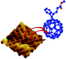
On this view porous polymer films32 would be promising candidates for controlling not only the horizontal but also the vertical nanostructure by filling them, in a tailored manner, with a second component. However, the established methods to obtain nanoscopic polymer pores are generally based on the self-assembly of block copolymers or polymer blends,33,34 thus they do not enable a precise control of the chemical composition of the film. It will be shown here that it is possible to obtain narrowly dispersed nanoporous homopolymer ultrathin films via the soft colloidal lithography35,36 and then to control their degree of filling. The method, schematized in Fig. 1A, consists of both the formation of a monolayer of hexagonally close packed silica nanoparticles and the filling of the monolayer interstices with a polymer film. Finally, by etching the silica nanoparticles with HF, polymer films with hexagonally close packed pores are obtained. These pores can be filled with a second organic component by spin coating and the degree of filling can be controlled by varying the solution concentration and/or the spin rate. Our approach has been applied to the poly(3-hexylthiophene) (P3HT) and [6,6]-phenyl-C61-butyric acid methyl ester (PCBM) blend, in view of its extensive use as active layer in organic photovoltaics where a careful control of both in-plane and out-of-plane nanostructure is required for maximizing the efficiency.10,37,38


image file: c5ra26053a-f1.tif
Fig. 1 Schematic representation of the nanoparticles-template method to obtain nanoporous polymer film (A). AFM height image of the nanoparticles layer (B) and of the nanoporous P3HT film upon the nanoparticles etching (C). The hexagonal packing of the nanoparticles, kept even after their removal, is highlighted in red.

Fig. 1B and C show the atomic force microscopy (AFM) topographical images of the 147 nm nominal diameter silica nanoparticles monolayer and of the polymer film after the silica etching. As it is evident, the porous structure keeps the same hexagonal array of the nanoparticles.

In order to verify that the HF etching does not affect the polymer chemical composition, an X-ray photoelectron spectroscopy (XPS) analysis, which allows to characterize both the elemental composition and the chemical bonds of polymer thin films,39,40 was performed on the porous P3HT film. These results were then compared to the ones of a flat HF-untreated P3HT film (Fig. 2). Both wide and elemental high resolution scans do not show any significant change between flat and porous P3HT films. In particular, the wide scan of the HF-treated sample does not show any signal coming from silicon or oxygen, confirming that the etching quantitatively removes the silica particles. Moreover, the carbon and sulphur high resolution scans are virtually identical for both samples, ensuring that the HF treatment does not alter the P3HT chemical composition.


image file: c5ra26053a-f2.tif
Fig. 2 XPS wide scan (A), high resolution C 1s (B) and S 2p (C) scans of the nanoporous and flat P3HT films. The continuous red lines in the high resolution scans show the individual component of the peaks.

Once obtained the porous P3HT film, it is possible to fill the pores with PCBM provided that the PCBM solution does not dissolve the polymer film. However, this issue can be easily solved by dissolving the PCBM in dichloromethane, which does not dissolve P3HT.41 In order to ensure a homogeneous coverage and to control the degree of filling, PCBM was deposited via spin coating, enabling the control of the thickness of the deposited layer by tuning the spinning speed and the concentration of the spread solution. In Fig. 3 the AFM topographical images of the P3HT pores filled with PCBM at different concentrations and at two different spinning speeds are reported. It is clear, especially for low PCBM concentrations, that the spin coating process does not alter the hexagonal arrangements of the pores. Moreover, at a given spinning speed, the pores depth gradually decreases with increasing the PCBM concentration and only at 4.5 mg ml−1 the pores are not visible anymore. This trend is highlighted in Fig. 3I, where the depth of the pores as a function of the PCBM concentration is plotted, showing also that the spinning speed itself can be used to tune the amount of PCBM deposited at nanometric level. These results clearly show that, during the spin coating process, PCBM molecules are selectively deposited inside the pores and that it is possible to control the degree of filling, and therefore controlling the vertical nanostructure, by modulating the experimental parameters.


image file: c5ra26053a-f3.tif
Fig. 3 AFM height images of the nanoporous P3HT film filled at 1500 rpm with PCBM solutions of 1.5 (A), 2.2 (B), 3.0 (C) and 4.5 (D) mg ml−1. AFM height images of the nanoporous P3HT film filled at 1000 rpm with PCBM solutions of 1.5 (E), 2.2 (F), 3.0 (G) and 4.5 (H) mg ml−1. Depth of the nanopores measured from the AFM images as a function of the PCBM concentration for both 1500 and 1000 rpm spinning speeds (I).

In order to extract quantitative structural information from the whole film thickness, grazing incidence X-ray small angle scattering (GISAXS) analysis was performed. GISAXS is a well established method to characterize the bulk nanostructure of ultrathin films42 providing information on the size and shape of the nanostructured objects43 as well as on their mutual assembly,44 thus being perfectly complementary to pure surface techniques like AFM.

In Fig. 4A the experimental and simulated 2D GISAXS patterns of the silica particles monolayer are reported. The experimental pattern can be effectively simulated by considering a hexagonal array of nanoparticles having an average diameter of 147 ± 6 nm. This low polydispersity gives rise to the numerous form factor hemi-circular rings around the reflected beam. The hexagonal arrangement leads instead to the formation of many the structure factor rods, whose length (see ESI Fig. S1) is diagnostic of the presence of a 2D-ordered layer.45


image file: c5ra26053a-f4.tif
Fig. 4 Simulated (left) and experimental (right) GISAXS patterns of the nanoparticles monolayer (A), of the P3HT nanopores (B) and of the nanopores filled at 1500 rpm from PCBM solutions of concentration 1.5 (C), 2.2 (D), 3.0 (E) and 4.5 (F) mg ml−1. Above each GISAXS pattern the pictorial representation of the form factor employed for the simulation is reported. The red rectangle between the experimental and simulated patterns represents the beamstop. The experimental structure factor rods are highlighted by the yellow box to facilitate the vision.

It is finally worth to observe that the presence of higher orders structure factor rods are due to the large size of the 2D crystalline domains (around 10 μm2), demonstrating the effectiveness of spin-coating as fast and easy method to obtain large 2D crystalline colloidal monolayer.

Upon etching the silica particles, the GISAXS pattern drastically changes (Fig. 4B) and no form factor signal from residual silica is observed, thus confirming the quantitative removal of the silica by HF. The weak contrast between pores and the polymer, as well as the increased uncorrelated irregularities of the pores shape, cause the extinction of the pores form factor manifestation on the GISAXS image. On the other hand, the structure factor rods are kept, because the pores maintain the hexagonal packing. Since the incoming X-ray beam samples the whole film thickness, a careful analysis of the GISAXS pattern allows determining the position of the pores across the film thickness itself and, more importantly, whether the bottom of the pore is covered by the polymer or not. The best simulation of the pores pattern is obtained by simulating truncated spheroidal air nanoparticles, having a diameter of 40 nm and a height of 25 nm, embedded in a 25 nm P3HT thin film. This means that the bottom of the pore is in direct contact with the native silicon oxide and explains why the PCBM selectively goes inside the pores. Indeed, since the silicon oxide surface free energy is much higher than the P3HT one,46 the PCBM covers the residual exposed part of the substrate in order to minimize the overall surface free energy. The structural simulation also shows that the size distribution of the pores increases with respect to the silica particles (see Table 1), this is due to the inhomogeneous polymer coverage on the particle layer. This lack of homogeneity is mainly caused by the boundaries between nanoparticles ordered domains (see ESI Fig. S2), where thicker P3HT layers are deposited. Finally, in Fig. 4C–F the GISAXS patterns of the P3HT pores filled at 1500 rpm with different PCBM concentrations are reported. It is evident that, by increasing the PCBM concentration, the scattering signal decreases and the rods become fainter. This effect is highlighted in ESI Fig. S3, where the horizontal cuts of the pattern at Qz 0.028 Å−1 are reported: the pure porous P3HT film shows three structure factor rods while, by increasing the PCBM concentration, the signal becomes progressively weaker and, at PCBM 4.5 mg ml−1, only a very weak first order is observed. The main cause of this effect is the loss of electron density contrast when filling the organic P3HT pores with another organic component. Moreover, the increased polydispersity given by the pores filling also contributes to the signal weakening (see Table 1). An excellent agreement between GISAXS experimental and simulated patterns was obtained by considering truncated spheroidal core–shell particles, having a PCBM core and an air shell, embedded in the polymer matrix. The employed shell structural parameters were identical to the empty pore ones and were kept constant. The optimal core position was found to be on the bottom of the shell, thus confirming that PCBM effectively and uniformly fills the pores. Furthermore, its sizes were found to gradually increase with increasing the PCBM concentration (see Table 1), as a result of the gradual filling of the pores. The results of these simulations do not show, upon the spreading of the PCBM component, any significant increase of the thickness of the porous matrix, confirming the selective filling of the pores by PCBM.

Table 1 Diameter and depth of the P3HT pores and the PCBM filling cores obtained from the GISAXS simulations
  P3HT pores PCBM 1.5 mg ml−1 cores PCBM 2.2 mg ml−1 cores PCBM 3 mg ml−1 cores PCBM 4.5 mg ml−1 cores
Diameter (nm) 40 ± 6 20 ± 6 24 ± 6 32 ± 9 40 ± 12
Depth (nm) 25 ± 1.5 7 ± 1.8 10 ± 2 20 ± 6 25 ± 6


Conclusions

We have reported a simple patterning methodology allowing to fully control the 3D nanostructures of polymer thin films. The method is based on the deposition of a nanoparticle monolayer that is used as a template to obtain nanoporous polymer films. The so-obtained pores can be then filled by a second component via spin coating and the degree of filling can be easily modulated by tuning the spinning speed and the concentration of the spread solution. This allows controlling with nanometre precision not only the in-plane nanostructure but also the out-of-plane one, and in turn the film chemical composition. We believe that our approach can be used to obtain fully controlled nanostructured polymer films enabling new experiments involving nano-confined soft matter. Moreover, the proper choice of the porous polymer and of the filling material will enable the preparation of a number of different 3D nanostructured polymeric and hybrid devices with great potential in many applications including membranes, electronics, photovoltaics, optical coatings, catalysis and sensing, among many other examples.

Acknowledgements

GL acknowledges the Surface Science Laboratory of the ESRF for AFM allocation and experimental support. AMG acknowledges Fapesp (processes 2013/13149-2 and 2011/19952-6) for financial support.

References

  1. R. D. Priestley, C. J. Ellison, L. J. Broadbelt and J. M. Torkelson, Science, 2005, 309, 456 CrossRef CAS PubMed.
  2. H. Atarashi, H. Morita, D. Yamazaki, M. Hino, T. Nagamura and K. Tanaka, J. Phys. Chem. Lett., 2010, 1, 881 CrossRef CAS.
  3. G. Li Destri, F. Miano and G. Marletta, Langmuir, 2014, 30, 3345 CrossRef CAS PubMed.
  4. S. K. Gupta, P. Jha, A. Singh, M. M. Chehimi and D. K. Aswal, J. Mater. Chem. C, 2015, 3, 8468 RSC.
  5. Y. Yang, K. Mielczarek, M. Aryal, A. Zakhidov and W. Hu, Nanoscale, 2014, 6, 7576 RSC.
  6. K. Sandvold Beckwith, S. P. Cooil, J. W. Wells and P. Sikorski, Nanoscale, 2015, 7, 8438 RSC; L. Xia, Z. X. Wei and M. X. Wan, J. Colloid Interface Sci., 2010, 341, 1 CrossRef CAS PubMed.
  7. G. Barbarella and F. Di Maria, Acc. Chem. Res., 2015, 48, 2230 CrossRef CAS PubMed.
  8. F. Brétagnol, A. Valsesia, G. Ceccone, P. Colpo, D. Gilliland, L. Ceriotti, M. Hasiwa and F. Rossi, Plasma Processes Polym., 2006, 3, 443 CrossRef.
  9. Y. Y. Kim, B. Ahn, S. Sa, M. Jeon, S. V. Roth, S. Y. Kim and M. Ree, Macromolecules, 2013, 46, 8235 CrossRef CAS.
  10. N. E. Jackson, B. M. Savoie, T. J. Marks, L. X. Chen and M. A. Ratner, J. Phys. Chem. Lett., 2015, 6, 77 CrossRef CAS PubMed.
  11. A. C. Shi and B. Li, Soft Matter, 2013, 9, 1398 RSC.
  12. I. P. Campbell, G. J. Lau, J. L. Feaver and M. P. Stoykovich, Macromolecules, 2012, 45, 1587 CrossRef CAS.
  13. R. J. Kline, M. D. McGehee and M. F. Toney, Nat. Mater., 2006, 5, 222 CrossRef.
  14. G. Li Destri, T. F. Keller, M. Catellani, F. Punzo, K. D. Jandt and G. Marletta, Langmuir, 2012, 28, 5257 CrossRef CAS PubMed.
  15. R. Schulze, M. M. L. Arras, G. Li Destri, M. Gottschaldt, J. Bossert, U. S. Schubert, G. Marletta, K. D. Jandt and T. F. Keller, Macromolecules, 2012, 45, 4740 CrossRef CAS.
  16. C. K. Shelton and T. H. Epps, Macromolecules, 2015, 48, 4572 CrossRef CAS.
  17. C. F. Shih, K. T. Hung, J. W. Wu, C. Y. Hsiao and W. M. Li, Appl. Phys. Lett., 2009, 94, 143505 CrossRef.
  18. A. Laiho, R. H. A. Ras, S. Valkama, J. Ruokolainen, R. Österbacka and O. Ikkala, Macromolecules, 2006, 39, 7648 CrossRef CAS.
  19. I. Botiz, A. B. F. Martinson and S. B. Darling, Langmuir, 2010, 26, 8756 CrossRef CAS PubMed.
  20. S. Y. Choi, J. U. Lee, J. W. Lee, S. Lee, Y. J. Song, W. H. Jo and S. H. Kim, Macromolecules, 2011, 44, 1771 CrossRef CAS.
  21. A. Takahashi, Y. Rho, T. Higashihara, B. Ahn, M. Ree and M. Ueda, Macromolecules, 2010, 43, 4843 CrossRef CAS.
  22. E. J. W. Crossland, M. Kamperman, M. Nedelcu, C. Ducati, U. Wiesner, D. M. Smilgies, G. E. S. Toombes, M. A. Hillmyer, S. Ludwigs, U. Steiner and H. J. Snaith, Nano Lett., 2009, 9, 2807 CrossRef CAS PubMed.
  23. I. Botiz and S. B. Darling, Macromolecules, 2009, 42, 8211 CrossRef CAS.
  24. P. D. Topham, A. J. Parnell and R. C. Hiorns, J. Polym. Sci., Part B: Polym. Phys., 2011, 49, 1131 CrossRef CAS.
  25. S. B. Darling, Prog. Polym. Sci., 2007, 32, 1152 CrossRef CAS.
  26. H. S. Wang, S. Y. Chen, M. H. Su, Y. L. Wang and K. H. Wei, Nanotechnology, 2010, 21, 145203 CrossRef PubMed.
  27. K. M. Coakley and M. D. McGehee, Appl. Phys. Lett., 2003, 83, 3380 CrossRef CAS.
  28. W. C. Yen, Y. H. Lee, J. F. Lin, C. A. Dai, U. S. Jeng and W. F. Su, Langmuir, 2011, 27, 109 CrossRef CAS PubMed.
  29. I. Martin-Fabiani, E. Rebollar, S. Perez, D. R. Rueda, M. C. Garcia-Gutierrez, A. Szymczyk, Z. Roslaniec, M. Castillejo and T. A. Ezquerra, Langmuir, 2012, 28, 7938 CrossRef CAS PubMed.
  30. S. Y. Kim, A. Nunns, J. Gwyther, R. L. Davis, I. Manners, P. M. Chaikin and R. A. Register, ACS Nano, 2014, 14, 5698–5705 CAS.
  31. Y. Morikawa, T. Kondo, S. Nagano and T. Seki, Chem. Mater., 2007, 19, 1540 CrossRef CAS.
  32. Y. Zhang, J. L. Sargent, B. W. Boudouris and W. A. Phillip, J. Appl. Polym. Sci., 2015, 132, 41683 Search PubMed.
  33. J. Gong, A. Zhang, H. Bai, Q. Zhang, C. Du, L. Li, Y. Hong and J. Li, Nanoscale, 2013, 5, 1195 RSC.
  34. T. Pietsch, P. Müller-Buschbaum, B. Mahltig and A. Fahmi, ACS Appl. Mater. Interfaces, 2015, 7, 12440 CAS.
  35. T. Chen, D. P. Chang, R. Jordan and S. Zauscher, Beilstein J. Nanotechnol., 2012, 3, 397 CrossRef PubMed.
  36. J. Zhang, Y. Li, X. Zhang and B. Yang, Adv. Mater., 2010, 22, 4249 CrossRef CAS PubMed.
  37. C. Lorch, H. Frank, R. Banerjee, A. Hinderhofer, A. Gerlach, G. Li Destri and F. Schreiber, Appl. Phys. Lett., 2015, 107, 201903 CrossRef.
  38. T. Kassar, N. S. Güldal, M. Berlinghof, T. Ameri, A. Kratzer, B. C. Schroeder, G. Li Destri, A. Hirsch, M. Heeney, I. McCulloch, C. J. Brabec and T. Unruh, Adv. Energy Mater., 2015 DOI:10.1002/aenm.201502025.
  39. N. Seidler, G. M. Lazzerini, G. Li Destri, G. Marletta and F. Cacialli, J. Mater. Chem. C, 2013, 1, 7748 RSC.
  40. K. Siow, S. Kumar and H. Griesser, Plasma Processes Polym., 2015, 32, 8 CrossRef.
  41. C. W. Rochester, S. A. Mauger and A. J. Moule, J. Phys. Chem. C, 2012, 116, 7287 CAS.
  42. M. Schwartzkopf, A. Buffet, V. Körstgens, E. Metwalli, K. Schlage, G. Benecke, J. Perlich, M. Rawolle, A. Rothkirch, B. Heidmann, G. Herzog, P. Müller-Buschbaum, R. Röhlsberger, R. Gehrke, N. Stribeck and S. V. Roth, Nanoscale, 2013, 5, 5053 RSC.
  43. M. Schwartzkopf, G. Santoro, C. J. Brett, A. Rothkirch, O. Polonskyi, A. Hinz, E. Metwalli, Y. Yao, T. Strunskus, F. Faupel, P. Müller-Buschbaum and S. V. Roth, ACS Appl. Mater. Interfaces, 2015, 7, 13547 CAS.
  44. I. Martín-Fabiani, E. Rebollar, M. C. García-Gutiérrez, D. R. Rueda, M. Castillejo and T. A. Ezquerra, ACS Appl. Mater. Interfaces, 2015, 7, 3162 Search PubMed.
  45. G. Li Destri, A. A. M. Gasperini and O. Konovalov, Langmuir, 2015, 31, 8856 CrossRef CAS PubMed.
  46. G. Li Destri, T. Keller, M. Catellani, F. Punzo, K. D. Jandt and G. Marletta, Macromol. Chem. Phys., 2011, 212, 905 CrossRef CAS.

Footnote

Electronic supplementary information (ESI) available: Materials and experimental methods, full 2D GISAXS pattern of the silica nanoparticles monolayer and of the porous pure P3HT film, 25 μm2 AFM height image of the nanoparticles monolayer, GISAXS cuts at Qz 0.28 Å−1 of the porous P3HT films with different degrees of PCBM filling. See DOI: 10.1039/c5ra26053a

This journal is © The Royal Society of Chemistry 2016
Click here to see how this site uses Cookies. View our privacy policy here.