
 Open Access Article
 This Open Access Article is licensed under a
 Creative Commons Attribution 3.0 Unported Licence
Generation of open-ended, worm-like and graphene-like structures from layered spherical carbon materials†
Bridget K. Mutumaa,
Boitumelo Matsosoa,
Kamalakannan Ranganathana,
Daniel Wamwangib and
Neil J. Coville*a
aDST-NRF Centre of Excellence in Strong Materials and Molecular Sciences Institute, School of Chemistry, University of the Witwatersrand, WITS 2050, Johannesburg, South Africa. E-mail: Neil.coville@wits.ac.za; Fax: +27 11717 6749
bDST-NRF Centre of Excellence in Strong Materials and Materials Physics Research Institute, School of Physics, University of the Witwatersrand, WITS 2050, Johannesburg, South Africa
First published on 5th February 2016
Abstract
A study of the effects of size dispersion of Au@SiO2 spheres and silica sphere templates for the synthesis of hollow carbon structures was evaluated using a chemical vapor deposition (CVD) nanocasting method. The diameter of the template, the presence of the gold nanoparticles and the polyvinylpyrrolidone (to cap the Au particles) were found to determine the size, thickness and shape of the synthesized carbon nanostructures. The Au@monodispersed small-sized silica sphere (80–110 nm) template covered with carbon followed by removal of silica produced broken hollow carbon spheres, whereas an equivalent Au@monodispersed large-sized silica sphere (110–150 nm) template produced hollow carbon spheres with a complete carbon shell. Monodispersed and polydispersed pristine silica spheres without Au produced hollow carbon spheres with complete and deformed carbon shells, respectively. Polyvinylpyrrolidone addition to polydispersed SiO2 spheres, followed by carbonization with toluene (1 h) and SiO2 removal, produced wormlike carbon structures. Carbonization (and SiO2 removal) of Au@polydispersed silica spheres for a short carbonization time (1 h) gave a layered carbon nanosheet while at intermediate and longer carbonization times (2–4 h) gave nanotube-like (or worm-like) carbon structures. Raman spectra confirmed the formation of the graphitic nature of the carbon materials. These results highlight the potential use of Au@carbon coreshell structures for the generation of few layered graphene-like unusual nanostructures. As a proof of concept, the wormlike carbon structures were incorporated in organic solar cells and found to give a measurable photovoltaic response.
1. Introduction
Layered graphene structures can in principle be made by two approaches – by a bottom-up approach from carbon building blocks or by top-down approaches from layered carbon materials. The bottom-up approach entails the synthesis of graphene structures by epitaxial growth of graphene sheets through Diels–Alder polymerization,1,2 layer by layer assembly,3 solvothermal4 and chemical vapor deposition methods. The chemical vapor deposition (CVD) methodology can entail depositing carbon on a metal template with some or limited carbon solubility such as Cu,5–7 Ni,8,9 and Co10 among others. The metal template acts as a catalyst for graphene layer formation and growth. In some cases, a catalyst free plasma enhanced chemical vapor deposition method, has been used to produce carbon nanosheets and vertically oriented graphene sheets.11–15 The top-down approach involves the exfoliation of graphite by mechanical, electrochemical or chemical means to give graphene.16,17 Indeed, the classical methodology to make graphene is from graphite.18 In principle any carbon source (planar, non-planar geometries) that contain layers of carbon atoms could be converted to an open layered carbon material. For instance, unzipping multiwalled carbon nanotubes can result in the formation of graphene oxide nanoribbons19 and graphene nanoribbons.20 A recent report has indicated that C60 can be converted into graphene quantum dots showing the possibility of creating graphene like structures from spherical carbon materials.21Typically, carbon nanomaterials are classified based on their dimensionalities such as zero-dimensional fullerenes (0D), one-dimensional carbon nanotubes (1D), two-dimensional graphenes (2D) and various three-dimensional structures (3D) respectively.22–25 The 3D carbon based nanostructures such as 3D graphene based composites and 3D porous carbons of high mechanical and structural stability, high electrical conductivity and large pore volume have been extensively studied.26–31 The hard template route has been used to synthesize various 3D carbon frameworks for energy applications.32–34 In addition, these nanostructures could be used as electron acceptors in polymer based solar cells due to their high interfacial area.
Hollow carbon spheres (HCSs) contain graphite like structures in their carbon shells. Because of these features they have been used extensively in fuel cells,35,36 as catalysts support,37,38 and in supercapacitors.39,40 This is due to their large pore volume, high surface area and the ability to tailor the diameters of the carbon shells. These nanostructured materials have been synthesized by hydrothermal carbonization,41 templating,42,43 Kirkendall effect, Ostwald ripening and the galvanic replacement methods among others.44 A hard templating method offers the ability to modify surface properties of templates, to manipulate the morphology and structure of the final product and to use readily available precursors.45 The carbon shell thickness can be controlled by varying the surfactant to precursor ratio,46,47 the amount of the carbon source48 and the carbonization time.49 To date, the carbon shell of a HCS is generally retained in the synthesis strategies employed. However, studies have indicated that structural collapse of a HCS can occur to produce broken shell structures.49–51
Organic solar cell (OSC), devices that convert solar energy into electrical energy often use semiconducting polymers made from carbon. Carbon is cheap, readily available, easily processable and is hydrophobic. This latter property ensures its compatibility with organic polymers used in the active layer when common organic solvents are used to make solar cell devices. In a bulk heterojunction (BHJ), the active layer comprises of an interpenetrating network of the p-type donor (poly(3-hexyl-thiophene-2,5-diyl), P3HT) and an n-type acceptor ([6,6]-phenyl-C61-butyric acid methyl ester, PCBM) respectively. The key component here is the fullerene that is a single layered spherical carbon material. Other hollow carbon nanostructures can also act as the electron accepting materials and be used to form a ternary blend of the active layer. In this approach metallic impurities in the carbon material are not present as HCS synthesis, unlike carbon nanotube synthesis, requires no catalyst.52–58 These early studies indicated that a key feature was the graphitic carbon network. To further explore the role of graphitic carbon structures in solar cell devices the use of “collapsed” HCSs has been explored. This is overcomes the issue associated with large HCSs that can conform to the size of the typical active layer dimensions of the OSC device and can lead to shorting. Graphene based nanostructures have been mainly used as electrode materials in organic and dye sensitized solar cells.59–61 In contrast, carbon nanotubes have been employed in the active layer to improve the efficiency of photovoltaic devices but owing to their metallic character favor charge carrier recombination.62–65 To our knowledge, the use of open ended worm like carbon nanostructures to form an active layer composite in organic solar cells has to date not been reported.
In this report, carbon has been deposited on monodispersed and polydispersed silica templates in the presence of Au nanoparticles embedded in the silica to produce graphene-like layered structures (Au@HCS). Hollow carbon spheres with broken spherical shells were produced from small and monodispersed SiO2 spheres and unusual open ended worm like layered structures were made from polydispersed silica sphere templates. In essence, the conversion of spherical core shell materials to an open ended worm like carbon nanostructures (3D) with unique morphologies by a CVD nanocasting method (a hard template route). The effect of Stober sphere diameter, polydispersion and carbonization time on the morphology of the carbon spheres produced as well as the role of the Au nanoparticles and the polyvinylpyrrolidone (PVP) used to cap the Au particles were studied. The obtained wormlike carbon nanostructures and the broken hollow/deformed carbon structures were employed in a ternary blend active layer to fabricate an organic solar cell.
2. Experimental
2.1 Starting materials
Tetraethyl orthosilicate, TEOS (98%, Aldrich), ammonium hydroxide, NH4OH (25% Fluka), ethanol (Merck 96%) and deionized water were used as reagents for the synthesis of the silica spheres. Hydrofluoric acid, (HF; 40%, Associated Chemical) was used for silica removal, and toluene (Aldrich) was used as a carbon source. Chloroauric acid, HAuCl4·3H2O (99.99%, Aldrich), polyvinylpyrrolidone, PVPK30 (Mw 40![[thin space (1/6-em)]](https://www.rsc.org/images/entities/char_2009.gif) 000, Aldrich), and trisodium citrate dihydrate were used as reagents for the synthesis of gold nanoparticles.
000, Aldrich), and trisodium citrate dihydrate were used as reagents for the synthesis of gold nanoparticles.
2.2 Synthesis of silica spheres and hollow carbon spheres (HCSs)
Monodispersed SiO2 spheres were synthesized by mixing 90 mL of ethanol, 63 mL of distilled water and 5 mL of NH4OH and the solution stirred for ten minutes. Then 16 mL of TEOS was added rapidly and the mixture stirred for 1 hour. In contrast, polydispersed SiO2 spheres were obtained by adding 2 mL of TEOS slowly to ethanol (40 mL) and 2 mL of NH4OH and the mixture allowed to stir for 1 h. The solutions were centrifuged at 4500 rpm for 20 minutes and the product dried at 80 °C for 12 hours. Carbonization of both the monodispersed and polydispersed SiO2 spheres was carried out by a bubbling method using toluene as the carbon source and argon as the carrier gas in a chemical vapor deposition reactor for 1 h, 2 h and 4 h respectively66 (Table 1). The carbonized silica was then etched with 10% HF for 24 hours at room temperature and dried to give the hollow carbon spheres.| Starting SiO2 material | SiO2 (nm) | CVD carbonization time (h) | Carbon shell thickness (nm) |
|---|---|---|---|
| Monodispersed SiO2 | 400–500 | 1 | 12 ± 5 |
| 2 | 38 ± 8 | ||
| 4 | 47 ± 10 | ||
| Polydispersed SiO2 | 90–310 | 1 | 8 ± 2 |
| 2 | 10 ± 3 | ||
| 4 | 32 ± 8 |
2.3 Synthesis of Au nanoparticles
HAuCl4·3H2O (0.01 M, 5 mL) was stirred at reflux for 30 minutes and trisodium citrate dihydrate (50 mL of 0.01 M) was added to the Au solution and the mixture stirred for 30 minutes. Polyvinylpyrrolidone (PVP; 0.5 g) was dissolved in 20 mL of distilled water and added dropwise to the Au solution and stirred at room temperature for 12 hours. Centrifugation at 12000 rpm for 15 minutes gave a suspension of gold nanoparticles (d = 14 ± 4 nm) in solution (Fig. S1†).
2.4 Synthesis of Au@SiO2 spheres
Gold@silica spheres were synthesized using the conditions shown in Table 2. Gold nanoparticles (2 mL, 0.00016 M) were mixed with 20 mL of ethanol and 0.5 mL of ammonia solution (25 wt%). The solutions were stirred for 20 minutes and then 1 mL of TEOS was added rapidly and the solutions stirred separately for 30 minutes and 1 hour respectively. The two solutions were then centrifuged for 20 minutes at 3500 rpm and the collected solids dried at 80 °C for 12 hours to give monodispersed Au@SiO2A and Au@SiO2B spheres respectively. Polydispersed Au@SiO2 particles were made by adding gold nanoparticles (20 mL) to 40 mL of ethanol and 2 mL of ammonia solution (25 wt%). The solution was stirred for 20 minutes and 2 mL of TEOS was added slowly and the solution stirred for 1 hour, centrifuged for 20 minutes at 3500 rpm and the collected solid dried at 80 °C for 12 hours to give Au@SiO2C.| Description | Stirring time (h) | Gold nanoparticle solution (mL) | Ethanol (mL) | Ammonia solution 25 wt% (mL) | TEOS (mL) |
|---|---|---|---|---|---|
| Au@SiO2A | 0.5 | 2 | 20 | 0.5 | 1 |
| Au@SiO2B | 1 | 2 | 20 | 0.5 | 1 |
| Au@SiO2C | 1 | 20 | 40 | 2 | 2 |
2.5 Synthesis of Au@hollow carbon structures (Au@HCSs)
Au@hollow carbon spheres (Au@HCSs) were synthesized by carbonization of the synthesized Au@SiO2 spheres in a horizontal chemical vapor deposition reactor. In separate reactors, the three Au@SiO2 samples (0.06 g) were uniformly spread onto a quartz boat which was placed in the center of a quartz tube. The furnace was heated to 900 °C at 10 °C min−1 under an Ar atmosphere (Ar, 200 sccm). Once the desired temperature was reached, Ar (200 sccm) was bubbled through toluene for 1 h for Au@SiO2A and Au@SiO2B and for 1 h, 2 h and 4 h for Au@SiO2C (to give Au@SiO2C1, Au@SiO2C2 and Au@SiO2C4) respectively. After this, the gas flow was stopped and the system was left to cool down to room temperature under an inert atmosphere (Ar, 200 sccm). The quartz boat was then removed from the reactor and the silica was removed with a 10% HF solution (24 hours) and after thorough washing with distilled water the product was dried at 80 °C for 12 hours to give the five Au@HCS samples (Table 3).| Description | Starting SiO2 material | SiO2 (nm) | Au (nm) | CVD carbonization time (h) | Morphology | Carbon shell thickness (nm) | Au (nm) |
|---|---|---|---|---|---|---|---|
| Au@HCSA | Au@SiO2A | 80–110 | 14 ± 3 | 1 | HCSs with broken shells | 8 ± 3 | 15 ± 4 |
| Au@HCSB | Au@SiO2B | 110–150 | 14 ± 4 | 1 | HCSs with complete shells | 8 ± 2 | 15 ± 6 |
| Au@HCSC1 | Au@SiO2C | 90–300 | 16 ± 4 | 1 | Layered graphene-like nanostructures | 13 ± 2 | 15 ± 4 |
| Au@HCSC2 | Au@SiO2C | 90–300 | 16 ± 4 | 2 | Open ended tube like nanostructures | 25 ± 5 | 16 ± 4 |
| Au@HCSC4 | Au@SiO2C | 90–300 | 16 ± 4 | 4 | Open ended tube like nanostructures | 38 ± 10 | 21 ± 6 |
2.6 Characterization
The morphology of the synthesized gold nanoparticles, Au@SiO2, Au@HCSs, pristine SiO2 and the HCSs was ascertained by transmission electron microscopy (TEM) using a FEI Technai G2 spirit electron microscope operating at 120 kV. Graphitic domains in Au@HCS were determined using a JEOL JEM 2100 High Resolution TEM (JEOL, Japan) fitted with a LaB6 gun. Images were captured at 200 kV using a Gatan Ultrascan camera (Gatan, USA). Samples were made by placing a droplet of suspended nanoparticles in ethanol on carbon coated grids and allowed to dry at room temperature. A Jobin Yvon T64000 Raman spectrometer equipped with an Ar ion laser (514.5 nm) and a laser power of 5 mW was used to establish the graphitic nature of the carbon found in the Au@HCSs and HCSs.3. Results and discussion
3.1 Silica spheres and hollow carbon spheres (HCSs)
Stober silica spheres were synthesized by classical routes.67 The silica spheres were made using two different reactant concentrations and reaction times to give monodispersed and polydispersed SiO2 with different sizes as shown in Fig. S2.† Monodispersed SiO2 spheres (400–500 nm) were obtained when TEOS was added quickly while polydispersed SiO2 spheres (90–310 nm) were obtained when TEOS was added slowly. A quick addition of TEOS results in the creation of nucleation sites at the same rate and time whereas a slow addition creates new nucleation site with each TEOS portion added, analogous to an interrupted particle growth mechanism.68,69 These spheres were carbonized with toluene for 1 h, 2 h and 4 h and the SiO2 was removed with HF to give HCSs (Table 1). The TEM images of the six different HCSs are shown in Fig. 1. It is noted that the HCSs were smaller in diameter than the SiO2 spheres due to the shrinkage of the silica spheres.37,70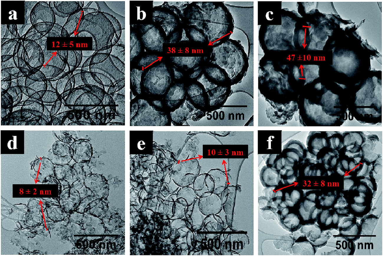 | ||
| Fig. 1 TEM images of hollow carbon spheres; (a–c) from monodispersed SiO2 spheres and (d–f) from polydispersed SiO2 spheres after (1 h, 2 h, 4 h) carbonization times and SiO2 removal respectively. | ||
For all types of silica spheres used, carbon coverage on SiO2 was observed prior to etching. The carbon shell thickness increased with increasing carbonization time as shown in Table 1. After treatment of the SiO2@C materials with HF, it is seen that the carbon shells in monodispersed HCSs retained their spherical shape (Fig. 1a–c). In contrast, HCSs with deformed and interconnected carbon shells were obtained after treatment of the polydispersed SiO2@C materials with HF (Fig. 1d and e). However, HCSs with complete carbon shells were obtained after 4 h carbonization of polydispersed SiO2 materials and SiO2 removal (Fig. 1f). Also to note: the carbon shell thickness of the polydispersed HCSs was thinner than that of the monodispersed HCSs. Though both mono and polydispersed SiO2 are chemically the same, SiO2 polydispersity was found to reduce the number of carbonization layers. This could be attributed to the packing of polydispersed particles which restricts toluene infiltration between SiO2 spheres during carbon shell growth on SiO2.
3.2 Au@SiO2 and Au@hollow carbon spheres
Au@SiO2 was made by classical procedures by dispersing Au particles in a solution containing TEOS (Table 2). The sizes of encapsulated gold nanoparticles were almost the same in all the Au@SiO2 spheres with a slight increase in size observed in Au@HCSs obtained after carbonization and SiO2 removal (Table 3). Fig. 2 show the TEM images of Au@SiO2A and Au@SiO2B templates with their respective HCS morphologies obtained after 1 h carbonization. The longer reaction time (1 h versus 0.5 h) used in the formation of the template gave a larger HCS as expected.71,72 Carbonization of the smaller sized silica spheres (Au@SiO2A) produced broken hollow carbon spheres after etching away the SiO2 (Fig. 2c) while the large sized silica sphere (Au@SiO2B; 110–150 nm) gave more unbroken spherical carbon shells after HF etching (Fig. 2d). Though, the thickness of the carbon shells was similar after 1 h carbonization time; the smaller HCSs were more prone to break during the etching procedures, due to the large strains induced by the larger curvature which weaken upon SiO2 removal. Carbon shell thickness dependent collapse of Au@SiO2A is thus unavoidable due to the smaller diameter size.50,51 | ||
| Fig. 2 TEM images of (a) Au@SiO2A, (b) Au@SiO2B spheres before carbonization and (c) Au@HCSA and (d) Au@HCSB after 1 h carbonization time and SiO2 removal. | ||
Fig. 3a shows TEM images of polydispersed Au@SiO2C spheres after synthesis. After 1 h carbonization a thin carbon shell (11 ± 2 nm) covering the silica (Fig. S3†) is formed which led to a layered carbon nanostructure (Fig. 3b) after HF etching. This contrasts with the morphologies found for Au@HCSA and Au@HCSB as the collapse led to large sheets of carbon shells instead of a hemispherical curved surface. The carbonization of silica spheres to give thin carbon shells occurred where the silica cores interconnected and breaching presumably occurred where the silica spheres intersected. A short carbonization time (1 h) produced a layered carbon nanosheet like morphology due to limited nucleation densities and surface coverage. Carbonization for longer times (2 & 4 h) led to the formation of long nanotube/worm like morphology (length > 500 nm) (Fig. 3c and d). Table 3 shows that an increase in carbon shell thickness of Au@HCSC occurs with an increase in carbonization time.
 | ||
| Fig. 3 TEM images of (a) Au@SiO2C, (b–d) Au@HCSC obtained after (1 h, 2 h, 4 h) carbonization times and SiO2 removal respectively. | ||
Comparison of polydispersed Au@HCSC (Fig. 3) and polydispersed HCSs (Fig. 1) showed that in the absence of gold, HCSs with deformed and interconnected carbon shells were observed and no carbon nanosheet like morphology was noted. This implicates the presence of Au in the formation of the peculiar carbon structures. A more detailed analysis of Au@HCSC1 was obtained from HRTEM studies (Fig. 4). HRTEM images of the Au@HCSC1 revealed that the sample could be viewed as a carbon sheet (Fig. 4a) made of overlapping carbon layers formed from the extended array of hollow carbon structures (Fig. 4b). The extended array was in the form of discontinuous curved features portraying the wavy nature of the carbon sphere edge.73 The carbon structure appears to follow the curvature of the unzipped spheres (Fig. 4c). Further analysis of the ‘film’ indicates that the carbon ‘shell’ shows the presence of graphitic domains (Fig. 4d; d interlayer spacing = 0.344 nm) with short range ordering (Fig. 4e) over large parts of the carbon structure. The structure also indicates regions of amorphous carbon as confirmed by selected area electron diffraction (SAED) data (ESI Fig. S4†).
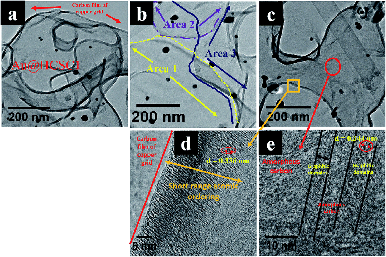 | ||
| Fig. 4 HRTEM images of Au@HCSC1; (a) shows the carbon film of Au@HCSC1 and that of the copper grid, (b) shows three overlapping areas of the carbon sheet (black spots are Au particles), (c) shows a folded region and a sheet like region with magnified images of (d) folded region and (e) sheet like region. | ||
The factors responsible for the formation of the wormlike carbon structures are described below.
To confirm the influence of PVP on the morphology of the obtained worm like and open ended carbon nanostructures, polydispersed SiO2 spheres (Fig. S2b) and PVP (20 mL) were mixed together and stirred for 1 hour and 12 hours respectively (see ESI†). The concentration of PVP was similar to that used in the synthesis of Au@SiO2C (for comparison purposes). Fig. S5a and S5b† shows the silica spheres mixed with PVP before carbonization confirming the PVP surface coverage on silica. The polydispersed silica spheres mixed with PVP after 1 h stirring time, followed by carbonization and SiO2 removal produced worm like hollow carbon nanostructures (Fig. S5c†). In contrast, a 12 hours stirring time, followed by carbonization and SiO2 removal gave broken hollow carbon spheres with a spherical morphology (Fig. S5d†). The carbon shell thickness was 7 ± 5 nm in the wormlike hollow structures and 9 ± 7 nm for the broken/deformed hollow carbon spheres. The wormlike carbon nanostructures had a unique hierarchical structure with the coexistence of mesopores and macropores within the non-spherical cavity as shown by the nitrogen adsorption–desorption isotherm (ESI Fig. S9†).
In the study, 900 °C was used for carbonization of the silica. Mixing of silica with PVP results in the presence of hydrogen bonded PVP polymer chains on SiO2 that carbonizes on the silica surface.79–81 Some of the PVP was lost due to sublimation at the reaction temperature. The surface morphology is dependent on the amount of PVP bound on the silica surface. When a high concentration of PVP was used on Au@SiO2 and polydispersed SiO2 spheres, a thin carbon nanosheet and wormlike hollow structures were obtained.
Fig. 5 shows a schematic diagram that summarizes the formation of the different carbon nanostructures for the Au@monodispersed and Au@polydispersed silica sphere templates. A small sized Au@monodispersed SiO2 sphere template results in Au@HCSs with breached shells while a large sized Au@SiO2 monodispersed sphere template gives Au@HCSs with complete shells. In contrast, the Au@polydispersed SiO2 sphere template gives graphene-like, wormlike and open ended tube like structures.
 | ||
| Fig. 5 Possible carbon nanostructure formation mechanism in (a) Au@SiO2A, (b) Au@SiO2B and (c) Au@SiO2C respectively. | ||
3.3 Raman spectra of hollow carbon spheres and Au@hollow carbon spheres
Table S1† shows the ID/IG ratios of monodispersed and polydispersed HCSs. The corresponding Raman spectra for HCSs and Au@HCSs are shown in Fig. S7 and S8.† In all cases, a strong D band was exhibited between 1342 cm−1 and 1381 cm−1 due to the breathing mode of sp2 and sp3 carbon atoms.83,84 In addition, a G peak was observed between 1575 cm−1 and 1597 cm−1 which is a characteristic of bond stretching of sp2 atoms. An increase in structural defects with increasing carbonization time was observed as seen from ID/IG ratios. This is expected as an increase in carbonization time increases the number of carbon atoms nucleating on the silica template leading to thicker carbon shells and thus more structural defects. Au@HCSA and Au@HCSC1 had fewer defects than Au@HCSB resulting in lower ID/IG ratios (Table S2†). A comparison of the Raman spectra of polydispersed Au@HCSs and HCSs shows a broad band between 2700 cm−1 and 2900 cm−1 characteristic of a 2D band. The broadness of the peak indicates the presence of large defects with small graphitic domains.85,86 In Au@HCSC1, D and G bands were observed at 1370 cm−1 and 1590 cm−1 respectively with a ID/IG ratio of 0.91, indicating less graphitic character. A broad 2D band was observed in Au@HCSC1 showing the presence of both graphitic and non-graphitic domains in agreement with the HRTEM results.3.4 Application of worm like hollow carbon nanostructures and broken HCSs in organic solar cells
The hollow carbon nanostructures (wormlike and broken HCSs) were mixed with P3HT and PCBM to form a ternary blend active layer (see ESI†). The pristine active layer (PCBM:P3HT blend) had a thickness of 190 ± 10 nm. Fig. S11† shows the AFM images of P3HT:PCBM:wormlike carbon nanostructures and P3HT:PCBM:broken HCSs with a surface roughness of 81.5 nm and 91.8 nm respectively. A PCBM absorption peak was observed at 336 nm and 338 nm for P3HT:PCBM with broken HCSs and wormlike HCSs respectively (Fig. 6).87 The absorption intensity of P3HT peaks were observed at 517 nm and at 553 nm/555 nm, with a shoulder (#) at 604 nm/605 nm in the films containing broken HCSs/wormlike HCSs respectively due to P3HT interchain π–π* interactions.88,89 The absorption intensity of the film comprising of P3HT:PCBM:wormlike HCSs was higher than that made of P3HT:PCBM:broken HCSs due to enhanced scattering of light. An increase in absorption intensity in the wormlike HCSs led to an increased short circuit current density (Jsc). The device performance is determined by the structural organization of the interpenetrating network, interface energy and self-assembly of active layer composites.90,91 Theoretical studies and experimental results of organic photovoltaic devices have shown that P3HT chains can self-assemble to wrap around the carbon based nanostructures and change the conjugation length of the P3HT to modify the device charge transfer properties.91,92 It is proposed that the large interface area provided in the open ended worm like structure could increase the interconnectivity to the P3HT chains and thus, alter the charge transfer properties in the active layer composite. | ||
| Fig. 6 UV-visible absorbance spectra of P3HT:PCBM:hollow carbon nanostructures films. | ||
Table 4 shows the current–voltage characteristics of the ternary blend active layer based organic solar cell under illumination and in the dark. An attempt to use hollow carbon spheres with a complete shell led to shorting of the photovoltaic devices due to their large diameter size. Hence, wormlike and broken HCSs were used. The current density of the device with wormlike HCSs is slightly higher than in the device with broken HCSs. This can be attributed to a reduced charge-transport distance, a slight increase in absorption intensity and less surface roughness in comparison to that of a device with broken HCSs. There was a slight increase in open circuit voltage (Voc) in the device with wormlike hollow carbon nanostructures which could be attributed to a change in the HOMO and LUMO energies of the active layer components.93–95 In addition, a possible charge carrier recombination is further corroborated by an S curve kink (see arrow in Fig. 7a) and by a high leakage current (Fig. 7b). The photovoltaic efficiency of the ternary solar cell fabricated using worm like structures was 0.11% while with broken hollow carbon spheres it was 0.14%. While these values are low they show an improvement with reference to the unbroken HCSs (see Fig. 7). The increase in shunt resistance, open circuit voltage and fill factor (FF) in P3HT:PCBM:broken HCSs relative to that of the device with wormlike HCSs were responsible for the slight improvement in photovoltaic efficiency.
| Description | Jsc (mA cm−2) | Voc (V) | Series resistance (ohms) | Shunt resistance (ohms) | FF (%) | Photovoltaic efficiency (%) |
|---|---|---|---|---|---|---|
| P3HT:PCBM:wormlike HCSs | 0.96 | 0.42 | 1.41 × 10⁴ | 6.07 × 10³ | 26.04 | 0.11 |
| P3HT:PCBM:broken HCSs | 0.73 | 0.50 | 5.95 × 10³ | 2.14 × 10⁴ | 37.26 | 0.14 |
 | ||
| Fig. 7 P3HT:PCBM:hollow carbon nanostructures current–voltage (J–V) curves (a) under illumination and (b) semi log J–V curves in the dark. | ||
4. Conclusions
This study provides insight into the effect of Au@polydispersed silica sphere templates and polydispersed SiO2 sphere templates towards the formation of hollow carbon nanostructures by a CVD nanocasting method, a study rarely performed. Au@HCSs and HCSs were successfully synthesized using a CVD nanocasting method with Au@SiO2 and SiO2 spheres as templates. The size of the Au@SiO2 and SiO2 templates used were found to play a key role in the synthesis of the hollow carbon spheres and nanostructures. Monodispersed and large sized Au@SiO2 spheres gave unbroken HCSs, whereas polydispersed Au@SiO2 spheres led to the formation of a range of hollow carbon nanostructures (thin carbon nanosheets and open ended nanotube like carbon). Modification of the surface chemistry of the polydispersed SiO2 using PVP was found to contribute to the worm like carbon nanostructures. Raman analysis confirmed the presence of the graphitized carbon in all the samples synthesized.The Au@HCS core shell layered materials have been used for the generation of graphene like open structures. The polydispersed SiO2 sphere functionalized with PVP generated worm like hollow carbon structures. The application of the wormlike nanostructures in organic solar cells opens new studies into the electronic properties of these materials. However, functionality of the P3HT on the wormlike nanostructures through self-assembly could lead to higher exciton dissociation. Further studies to check the effect of PVP concentration and addition to SiO2 spheres on carbon sphere morphology to explore the formation and growth control of these carbon nanostructures and their application in organic solar cells with optimized parameters is underway.
Acknowledgements
We thank the NRF, the University of Witwatersrand and the DST-NRF Centre of Excellence in Strong Materials for financial support. We thank the CSIR Nanocentre (Dr J Wesley Smith), Pretoria for assistance with the HRTEM measurements.References
- Y. Byun and A. Coskun, Chem. Mater., 2015, 27, 2576–2583 CrossRef CAS.
- A. Narita, I. A. Verzhbitskiy, W. Frederickx, K. S. Mali, S. A. Jensen, M. R. Hansen, M. Bonn, S. De Feyter, C. Casiraghi, X. Feng and K. Müllen, ACS Nano, 2014, 8, 11622–11630 CrossRef CAS PubMed.
- A. Kouloumpis, K. Spyrou, K. Dimos, V. Georgakilas, P. Rudolf and D. Gournis, Frontiers in Materials, 2015, 2, 10 CrossRef.
- Q. Kuang, S.-Y. Xie, Z.-Y. Jiang, X.-H. Zhang, Z.-X. Xie, R.-B. Huang and L.-S. Zheng, Carbon, 2004, 42, 1737–1741 CrossRef CAS.
- B. Hu, H. Ago, Y. Ito, K. Kawahara, M. Tsuji, E. Magome, K. Sumitani, N. Mizuta, K.-i. Ikeda and S. Mizuno, Carbon, 2012, 50, 57–65 CrossRef CAS.
- H. Kim, I. Song, C. Park, M. Son, M. Hong, Y. Kim, J. S. Kim, H.-J. Shin, J. Baik and H. C. Choi, ACS Nano, 2013, 7, 6575–6582 CrossRef CAS PubMed.
- Q. Wu, S. J. Jung, S. K. Jang, J. Lee, I. Jeon, H. Suh, Y. H. Kim, Y. H. Lee, S. Lee and Y. J. Song, Nanoscale, 2015, 7, 10357–10361 RSC.
- K. S. Kim, Y. Zhao, H. Jang, S. Y. Lee, J. M. Kim, K. S. Kim, J.-H. Ahn, P. Kim, J.-Y. Choi and B. H. Hong, Nature, 2009, 457, 706–710 CrossRef CAS PubMed.
- W. Liu, S. Kraemer, D. Sarkar, H. Li, P. M. Ajayan and K. Banerjee, Chem. Mater., 2014, 26, 907–915 CrossRef.
- H. Ago, Y. Ito, N. Mizuta, K. Yoshida, B. Hu, C. M. Orofeo, M. Tsuji, K.-i. Ikeda and S. Mizuno, ACS Nano, 2010, 4, 7407–7414 CrossRef CAS PubMed.
- J. Wang, M. Zhu, R. A. Outlaw, X. Zhao, D. M. Manos and B. C. Holloway, Carbon, 2004, 42, 2867–2872 CrossRef CAS.
- M. Zhu, J. Wang, B. C. Holloway, R. A. Outlaw, X. Zhao, K. Hou, V. Shutthanandan and D. M. Manos, Carbon, 2007, 45, 2229–2234 CrossRef CAS.
- M. Zhu, J. Wang, R. A. Outlaw, K. Hou, D. M. Manos and B. C. Holloway, Diamond Relat. Mater., 2007, 16, 196–201 CrossRef CAS.
- L. Zeng, D. Lei, W. Wang, J. Liang, Z. Wang, N. Yao and B. Zhang, Appl. Surf. Sci., 2008, 254, 1700–1704 CrossRef CAS.
- Z. Wang, M. Shoji and H. Ogata, Appl. Surf. Sci., 2011, 257, 9082–9085 CrossRef CAS.
- V. Eswaraiah, S. S. Jyothirmayee Aravind and S. Ramaprabhu, J. Mater. Chem., 2011, 21, 6800–6803 RSC.
- W. S. Hummers and R. E. Offeman, J. Am. Chem. Soc., 1958, 80, 1339 CrossRef CAS.
- A. K. Geim and K. S. Novoselov, Nat. Mater., 2007, 6, 183–191 CrossRef CAS PubMed.
- A. L. Higginbotham, D. V. Kosynkin, A. Sinitskii, Z. Sun and J. M. Tour, ACS Nano, 2010, 4, 2059–2069 CrossRef CAS PubMed.
- J. Li, S. Ye, T. Li, X. Li, X. Yang and S. Ding, Procedia Eng., 2015, 102, 492–498 CrossRef CAS.
- C. K. Chua, Z. Sofer, P. Šimek, O. Jankovský, K. Klímová, S. Bakardjieva, Š. Hrdličková Kučková and M. Pumera, ACS Nano, 2015, 9, 2548–2555 CrossRef CAS PubMed.
- H. Gleiter, Acta Mater., 2000, 48, 1–29 CrossRef CAS.
- V. V. Pokropivny and V. V. Skorokhod, Mater. Sci. Eng., C, 2007, 27, 990–993 CrossRef CAS.
- M. Terrones, A. R. Botello-Méndez, J. Campos-Delgado, F. López-Urías, Y. I. Vega-Cantú, F. J. Rodríguez-Macías, A. L. Elías, E. Muñoz-Sandoval, A. G. Cano-Márquez, J.-C. Charlier and H. Terrones, Nano Today, 2010, 5, 351–372 CrossRef.
- J. N. Tiwari, R. N. Tiwari and K. S. Kim, Prog. Mater. Sci., 2012, 57, 724–803 CrossRef CAS.
- X.-L. Wu and A.-W. Xu, J. Mater. Chem. A, 2014, 2, 4852–4864 CAS.
- H. Jiang, P. S. Lee and C. Li, Energy Environ. Sci., 2013, 6, 41–53 CAS.
- S. Mao, G. Lu and J. Chen, Nanoscale, 2015, 7, 6924–6943 RSC.
- Z. Yang, S. Chabi, Y. Xia and Y. Zhu, Progress in Natural Science: Materials International, 2015, 25, 554–562 CrossRef.
- L. Zhang and G. Shi, J. Phys. Chem. C, 2011, 115, 17206–17212 CAS.
- Z. Yang, C. Yan, J. Liu, S. Chabi, Y. Xia and Y. Zhu, RSC Adv., 2015, 5, 29397–29400 RSC.
- C. Wu, S. Deng, H. Wang, Y. Sun, J. Liu and H. Yan, ACS Appl. Mater. Interfaces, 2014, 6, 1106–1112 CAS.
- A. H. Lu and F. Schüth, Adv. Mater., 2006, 18, 1793–1805 CrossRef CAS.
- H.-J. Peng, J. Liang, L. Zhu, J.-Q. Huang, X.-B. Cheng, X. Guo, W. Ding, W. Zhu and Q. Zhang, ACS Nano, 2014, 8, 11280–11289 CrossRef CAS PubMed.
- C. Galeano, J. C. Meier, M. Soorholtz, H. Bongard, C. Baldizzone, K. J. J. Mayrhofer and F. Schüth, ACS Catal., 2014, 4, 3856–3868 CrossRef CAS.
- Z. Wen, Q. Wang, Q. Zhang and J. Li, Electrochem. Commun., 2007, 9, 1867–1872 CrossRef CAS.
- I. Nongwe, V. Ravat, R. Meijboom and N. J. Coville, Appl. Catal., A, 2013, 466, 1–8 CrossRef CAS.
- V. Ravat, I. Nongwe and N. J. Coville, ChemCatChem, 2012, 4, 1930–1934 CrossRef CAS.
- K. Wilgosz, X. Chen, K. Kierzek, J. Machnikowski, R. Kalenczuk and E. Mijowska, Nanoscale Res. Lett., 2012, 7, 1–5 CrossRef PubMed.
- X. Chen, K. Kierzek, K. Cendrowski, I. Pelech, X. Zhao, J. Feng, R. J. Kalenczuk, T. Tang and E. Mijowska, Colloids Surf., A, 2012, 396, 246–250 CrossRef CAS.
- M. Li, Q. Wu, M. Wen and J. Shi, Nanoscale Res. Lett., 2009, 4, 1365–1370 CrossRef CAS PubMed.
- J. B. Joo, P. Kim, W. Kim, J. Kim, N. D. Kim and J. Yi, Curr. Appl. Phys, 2008, 8, 814–817 CrossRef.
- P.-j. Cai and L. Feng, Mater. Chem. Phys., 2008, 108, 1–3 CrossRef CAS.
- H. C. Zeng, J. Mater. Chem., 2011, 21, 7511–7526 RSC.
- A.-H. Lu, G.-P. Hao, Q. Sun, X.-Q. Zhang and W.-C. Li, Macromol. Chem. Phys., 2012, 213, 1107–1131 CrossRef CAS.
- B. Fang, J. H. Kim, M.-S. Kim, A. Bonakdarpour, A. Lam, D. P. Wilkinson and J.-S. Yu, J. Mater. Chem., 2012, 22, 19031–19038 RSC.
- X. Chen, K. Kierzek, Z. Jiang, H. Chen, T. Tang, M. Wojtoniszak, R. J. Kalenczuk, P. K. Chu and E. Borowiak-Palen, J. Phys. Chem. C, 2011, 115, 17717–17724 CAS.
- Y. Dai, H. Jiang, Y. Hu, Y. Fu and C. Li, Ind. Eng. Chem. Res., 2014, 53, 3125–3130 CrossRef CAS.
- F. Su, X. S. Zhao, Y. Wang, L. Wang and J. Y. Lee, J. Mater. Chem., 2006, 16, 4413–4419 RSC.
- X. Xu and S. A. Asher, J. Am. Chem. Soc., 2004, 126, 7940–7945 CrossRef CAS PubMed.
- P. M. Arnal, F. Schuth and F. Kleitz, Chem. Commun., 2006, 1203–1205, 10.1039/B517196B.
- Y. Xia, Z. Yang and R. Mokaya, J. Phys. Chem. B, 2004, 108, 19293–19298 CrossRef CAS.
- C. Laurent, E. Flahaut, A. Peigney and A. Rousset, New J. Chem., 1998, 22, 1229–1237 RSC.
- M. Kim, S. B. Yoon, K. Sohn, J. Y. Kim, C.-H. Shin, T. Hyeon and J.-S. Yu, Microporous Mesoporous Mater., 2003, 63, 1–9 CrossRef CAS.
- K. Wilgosz, X. Chen, K. Kierzek, J. Machnikowski, R. J. Kalenczuk and E. Mijowska, Nanoscale Res. Lett., 2012, 7, 269 CrossRef PubMed.
- Y. Kanai and J. C. Grossman, Nano Lett., 2008, 8, 908–912 CrossRef CAS PubMed.
- Q. Sun, B. He, X.-Q. Zhang and A.-H. Lu, ACS Nano, 2015, 9, 8504–8513 CrossRef CAS PubMed.
- H.-J. Lu, Y. Li, L.-Q. Zhang, H.-N. Li, Z.-X. Zhou, A.-R. Liu, Y.-J. Zhang and S.-Q. Liu, RSC Adv., 2015, 5, 52126–52131 RSC.
- H. Park, S. Chang, M. Smith, S. Gradečak and J. Kong, Sci. Rep., 2013, 3, 1581 Search PubMed.
- Z. Liu, P. You, S. Liu and F. Yan, ACS Nano, 2015, 9, 12026–12034 CrossRef CAS PubMed.
- Y. Zhu, X. Meng, H. Cui, S. Jia, J. Dong, J. Zheng, J. Zhao, Z. Wang, L. Li, L. Zhang and Z. Zhu, ACS Appl. Mater. Interfaces, 2014, 6, 13833–13840 CAS.
- I. Khatri, S. Adhikari, H. R. Aryal, T. Soga, T. Jimbo and M. Umeno, Appl. Phys. Lett., 2009, 94, 093509 CrossRef.
- H. Derbal-Habak, C. Bergeret, J. Cousseau and J. M. Nunzi, Sol. Energy Mater. Sol. Cells, 2011, 95(1), S53–S56 CrossRef CAS.
- M. M. Stylianakis and E. Kymakis, Appl. Phys. Lett., 2012, 100, 093301 CrossRef.
- G. Keru, P. G. Ndungu, G. T. Mola, A. F. Nogueira and V. O. Nyamori, J. Nanomater., 2016, 2016, 11 Search PubMed.
- Y. D. Xia and R. Mokaya, Adv. Mater., 2004, 16, 886–891 CrossRef CAS.
- W. Stöber, A. Fink and E. Bohn, J. Colloid Interface Sci., 1968, 26, 62–69 CrossRef.
- V. Masalov, N. Sukhinina, E. Kudrenko and G. Emelchenko, Nanotechnology, 2011, 22, 275718 CrossRef CAS PubMed.
- K. Nozawa, H. Gailhanou, L. Raison, P. Panizza, H. Ushiki, E. Sellier, J. P. Delville and M. H. Delville, Langmuir, 2005, 21, 1516–1523 CrossRef CAS PubMed.
- J. H. Kim, B. Fang, M. Kim and J.-S. Yu, Catal. Today, 2009, 146, 25–30 CrossRef CAS.
- S. K. Park, K. D. Kim and H. T. Kim, Colloids Surf., A, 2002, 197, 7–17 CrossRef CAS.
- N. Jaramillo, C. Paucar and C. García, J. Mater. Sci., 2014, 49, 3400–3406 CrossRef CAS.
- X. H. Chen, F. M. Deng, J. X. Wang, H. S. Yang, G. T. Wu, X. B. Zhang, J. C. Peng and W. Z. Li, Chem. Phys. Lett., 2001, 336, 201–204 CrossRef CAS.
- J. T. G. Overbeek, Adv. Colloid Interface Sci., 1982, 15, 251–277 CrossRef CAS.
- A. Van Blaaderen, J. Van Geest and A. Vrij, J. Colloid Interface Sci., 1992, 154, 481–501 CrossRef CAS.
- M. T. Harris, R. R. Brunson and C. H. Byers, J. Non-Cryst. Solids, 1990, 121, 397–403 CrossRef CAS.
- S.-L. Chen, P. Dong, G.-H. Yang and J.-J. Yang, Ind. Eng. Chem. Res., 1996, 35, 4487–4493 CrossRef CAS.
- Y. Chung, M. Jeon and C. Kim, Macromol. Res., 2009, 17, 37–43 CrossRef CAS.
- V. M. Bogatyrev, N. V. Borisenko and V. A. Pokrovskii, Russ. J. Appl. Chem., 2001, 74, 839–844 CrossRef CAS.
- Y. K. Du, P. Yang, Z. G. Mou, N. P. Hua and L. Jiang, J. Appl. Polym. Sci., 2006, 99, 23–26 CrossRef CAS.
- F. Kooli, J. Chem., 2015, 2015, 8 Search PubMed.
- J. Luo, H. D. Jang and J. Huang, ACS Nano, 2013, 7, 1464–1471 CrossRef CAS PubMed.
- A. C. Ferrari, Solid State Commun., 2007, 143, 47–57 CrossRef CAS.
- F. Tuinstra and J. L. Koenig, J. Chem. Phys., 1970, 53, 1126–1130 CrossRef CAS.
- A. C. Ferrari and D. M. Basko, Nat. Nanotechnol., 2013, 8, 235–246 CrossRef CAS PubMed.
- A. Jorio, ISRN Nanotechnol., 2012, 2012, 16 Search PubMed.
- J. Liu, S. Shao, H. Wang, K. Zhao, L. Xue, X. Gao, Z. Xie and Y. Han, Org. Electron., 2010, 11, 775–783 CrossRef CAS.
- N. Kiriy, E. Jähne, H.-J. Adler, M. Schneider, A. Kiriy, G. Gorodyska, S. Minko, D. Jehnichen, P. Simon, A. A. Fokin and M. Stamm, Nano Lett., 2003, 3, 707–712 CrossRef CAS.
- H. Sirringhaus, P. J. Brown, R. H. Friend, M. M. Nielsen, K. Bechgaard, B. M. W. Langeveld-Voss, A. J. H. Spiering, R. A. J. Janssen, E. W. Meijer, P. Herwig and D. M. de Leeuw, Nature, 1999, 401, 685–688 CrossRef CAS.
- I. Botiz and N. Stingelin, Materials, 2014, 7, 2273 CrossRef CAS.
- C. Yang, J. G. Hu and A. J. Heeger, J. Am. Chem. Soc., 2006, 128, 12007–12013 CrossRef CAS PubMed.
- M. Bernardi, M. Giulianini and J. C. Grossman, ACS Nano, 2010, 4, 6599–6606 CrossRef CAS PubMed.
- I. Lange, J. Kniepert, P. Pingel, I. Dumsch, S. Allard, S. Janietz, U. Scherf and D. Neher, J. Phys. Chem. Lett., 2013, 4, 3865–3871 CrossRef CAS.
- S. Günes, H. Neugebauer and N. S. Sariciftci, Chem. Rev., 2007, 107, 1324–1338 CrossRef PubMed.
- C. J. Brabec, A. Cravino, D. Meissner, N. S. Sariciftci, T. Fromherz, M. T. Rispens, L. Sanchez and J. C. Hummelen, Adv. Funct. Mater., 2001, 11, 374–380 CrossRef CAS.
Footnote |
| † Electronic supplementary information (ESI) available. See DOI: 10.1039/c5ra25880d |
| This journal is © The Royal Society of Chemistry 2016 |