Growth and characterization of zeolitic imidazolate framework-8 nanocrystalline layers on microstructured surfaces for liquid crystal alignment

Lu-Jian Chen*ab, Bin Luoa, Wen-Song Lia, Can Yanga, Tao Yebd, Sen-Sen Lia, Xiao-Zhong Wanga, Yuan-Jing Cuibc, Han-Ying Libd and Guo-Dong Qianbc
aDepartment of Electronic Engineering, School of Information Science and Engineering, Xiamen University, Xiamen 361005, China. E-mail: lujianchen@xmu.edu.cn
bState Key Laboratory of Silicon Materials, Zhejiang University, Hangzhou, 310027, China
cCyrus Tang Center for Sensor Materials and Applications, Department of Materials Science and Engineering, Zhejiang University, Hangzhou, 310027, China
dMOE Key Laboratory of Macromolecular Synthesis and Functionalization, Department of Polymer Science and Engineering, Zhejiang University, Hangzhou, 310027, China

Received 3rd December 2015 , Accepted 8th January 2016

First published on 13th January 2016


Abstract

Zeolitic imidazolate framework-8 (ZIF-8) nanocrystalline layers were grown on carboxylate-terminated sol–gel films patterned with surface-relief microstructures. The coverage of ZIF-8 nanocrystals was significantly affected by the surface morphology, like the size and interspace of microstructures. Its vertically aligning ability to a typical nematic liquid crystal (LC) E7 was verified and its applications as a hybrid aligned nematic (HAN) LC cell-based voltage-dependent light modulator and a switchable diffraction grating were demonstrated.

1. Introduction

Metal–organic frameworks (MOFs) are porous crystalline materials in which metal ions are joined together by organic linkers, now attracting research interest for their potential use in gas storage, chemical catalysis and small molecule separations due to their high surface areas, large pore size, tunability and well-defined nanometer-scale cavities, and chemical tailorability.1–4 Some MOFs such as zeolitic imidazolate frameworks (ZIFs), which are a distinctive, rapidly developing sub-family of MOFs, display exceptional thermal and chemical stability and the rich structural diversity found in zeolites.5 In particular, ZIF-8 ((Zn(mIm)2, mIm = 2-methylimidazolate)), which crystallized with a sodalite (SOD)-related structure and featured large cavities (11.6 Å) and small apertures (3.4 Å), is one of the most studied prototypical ZIF compounds.6–10 In addition, many applications rely on the adherence of active MOF materials to organic and inorganic substrates.11–13 The ability to position and pattern MOF nano-/micro-structures on films allows diverse industrial applications.11–18 Many efforts have been made to achieve this goal, which can be generally classified into two categories: bottom-up approach and top-down approach.14 Among them, one of the most efficient ways is to functionalize the target surface using specific organic groups and promote the nucleation and growth of MOFs on top of it.15,16 It can be also combined with step-wise deposition technique, providing more precise control over selectively anchoring MOFs than the traditional solvothermal synthesis to achieve high quality patterns.11 However, only a few researches focused on the growth of MOFs on corrugated surfaces and the relationship with the specifically well-defined microstructures requires further investigations.

Furthermore, while MOFs nanocrystalline films or coatings are well promising for tremendous industrial applications, only a few of the optics-related works has been reported and drawn considerable attention for the development of chemical sensors for gases and small organic molecules. Up to now, a handful of luminescent MOF film-based sensors have been described.19–27 Very recently, a new optical transduction mechanism based on the tunability of the effective refractive index (neff) of MOFs via adsorption of guest molecules and the binding of specific analytes within the pores of the MOF films was explored. Furthermore, MOFs integrated label-free optical sensors based on Fabry–Pérot interference7,8 and one dimensional (1D) and three-dimensional (3D) photonic structures28–32 have been reported.

In practice, other than these properties of intrinsic luminescence and refractive index modulation, it is rarely reported that MOFs nanocrystalline films can be associated with light polarization, which is known as a significant issue and can be facilely realized to be controllable in liquid crystal (LC) devices with voltage-dependent features. All that needs is to fabricate LC alignment layers providing LC molecules with a specific orientation, which is critical to LC display (LCD) industry. Although the mechanically-rubbing and photo-alignment techniques have been intensively studied and commonly adopted, there still have alternative methods, mostly related to nanoparticles (NPs), which were developed to meet the specific requirements for beyond-display applications. Planar (homogeneous) alignment (PA) and vertical (homeotropic) alignment (VA) of LCs were obtained by doping or depositing NPs, e.g. Ni bowl-like NPs, polyhedral oligomeric silsesquioxane (POSS) NPs, Au NPs and CdSe NPs, etc., in the bulk LCs or on glass substrates, respectively.33–37 Several research groups also devoted to the investigation of new alignment technologies by synthesizing inorganic nanoporous anodic aluminium oxide (np-AAO) films and zinc oxide (ZnO) nanorods and nanowire arrays.38,39 These results inspired our exploration of seeking novel category of nanocrystalline materials, like the MOFs, with possible LCs aligning capabilities for light polarization-related applications.

Herein, we reported the growth of ZIF-8 nanocrystalline layers on carboxylate-terminated sol–gel films patterned by soft-lithography. The coverage ratio of ZIF-8 grains on the microstructured surfaces, with various stripe width and spacing between adjacent surface-relief stripes, is characterized by investigating the scanning electron microscope (SEM) morphology. The vertical alignment ability of the ZIF-8 nanocrystalline layer for nematic liquid crystal E7 is revealed and two potential applications as hybrid aligned nematic (HAN) LC cell-based voltage-dependent light modulator and switchable diffraction grating are demonstrated without and with microstructures, respectively.

2. Experimental

2.1 Materials

All solvents and chemicals were of reagent quality and used without further purification unless specified. Vinyltriethoxysilane (VTES) and tetraethoxysilane (TEOS) were purchased from Nanjing Qizheng Chemical. Co., Ltd. Poly(dimethylsiloxane) (PDMS, Sylgard 184) were purchased from Dow Corning. Zn(NO3)2·H2O, KMnO4, NaIO4 and methanol were purchased from Shantou Xilong Chemical Co., Ltd. 2-Methylimidazole (mIm) was purchased from Sigma-Aldrich. PVA (molecular weight 75[thin space (1/6-em)]000 g mol−1, alcoholysis degree 87–89%) were purchased from Shanghai Aladdin Reagent Co., Ltd. E7, which is a nematic LC mixture containing cyanobiphenyl and cyanoterphenol components at a specific composition, were obtained from Yantai Xianhua Chemical Co., Ltd.

2.2 Patterning of carboxylate-terminated sol–gel films

The detailed preparation process of ZIF-8 nanocrystalline layers on pristine (without microstructure), soft-lithography patterned (with microstructure) sol–gel films and the representation of ZIF-8 structure is shown in Fig. 1. The schematic illustration is described as follows. For siloxane precursors, vinyltriethoxysilane (VTES) and tetraethoxysilane (TEOS) at a molar ratio of 1[thin space (1/6-em)]:[thin space (1/6-em)]1 were mixed in ethanol solution. The molar ratio of the total deionized water to the precursor mixture was 2[thin space (1/6-em)]:[thin space (1/6-em)]1. The acidic water needed for hydrolysis (as dilute HCl solution, pH = 2) was introduced drop by drop to the stirring mixtures. After stirring for 45 min, miscibility is accomplished as the catalytic hydrolysis of the alkoxides proceeds. The mixture was aged for 48 hours and filtrated through a 0.2 μm membrane filter before film deposition. The inner surfaces of the indium-tin-oxide (ITO) glass substrates were cleaned and did not need any surface treatment. Wet sol–gel films were obtained on bare glass and ITO glass substrates by spin coating at 2000 rpm. Pristine films were soft baked at 90 °C for 1 hour. For the patterned ones, soft lithography technology based on PDMS was employed.40,41 A flexible PDMS elastomeric stamp was duplicated from the silicon master and pressed onto the fresh wet film. The assembly was allowed to dry and co-condensation at ambient temperature for a period of time, revealing the imprinted structures after stamp removal. The patterned sol–gel films were also baked at 90 °C for 1 hour to densify the microstructures.
image file: c5ra25794h-f1.tif
Fig. 1 The schematic illustration of fabrication process of sol–gel film by soft lithography, the growth of ZIF-8 nanocrystalline layer and the representation of ZIF-8 structure (blue polyhedral for Zn tetrahedra, green balls for nitrogen atoms, black balls for carbon atoms and hydrogen atoms are omitted).

Before the growth of ZIF-8 nanocrystalline layer, the vinyl groups on pristine and patterned sol–gel films have been oxidized to carboxylic acid groups according to a protocol described by Wasserman and coworkers.42 Briefly, the sol–gel films were suspended into an aqueous solution (40 ml) of KMnO4 (4 mg) and NaIO4 (168 mg) for 12 h.

2.3 Deposition of ZIF-8 layer

The substrates were alternately exposed to a freshly mixed solution containing the metal source Zn(NO3)2 and the organic linker mIm, with purging steps in between.7 500 ml methanolic stock solutions of Zn(NO3)2·H2O (25 mM) and of mIm (50 mM) were prepared. ZIF-8 thin films were obtained by immersing the carboxylate-terminated sol–gel films in a fresh mixture of 10 ml Zn(NO3)2 stock solution and 10 ml 2-methylimidazole (mIm) stock solution for 30 minutes at room temperature. Then they were washed with methanol and dried under nitrogen flow. With the repeated cyclic growth with freshly mixed reaction solutions, thicker films can be obtained. For comparison purpose, we only repeated the growth on both the pristine and patterned sol–gel films with different stripe width and spacing between adjacent surface-relief stripes. Unless specified, only 1 cycle growth of 30 min was employed.

2.4 Fabrication of LC glass cells

Three types of ITO glass cells with a suitable cell gap were prepared with different inner surfaces: (i) vertical aligned (VA) cell with a pair of ZIF-8 coated pristine sol–gel films, (ii) HAN cell with a PVA alignment layer facing a ZIF-8 coated pristine sol–gel film and (iii) HAN LC grating cell with a PVA alignment layer facing a ZIF-8 coated sol–gel film with surface-relief microstructures. The PVA surface was rubbed to induce LC orientation parallel to the ITO glass substrates. The rubbing direction is parallel to the grating stripes in the HAN LC grating cell. The cells, infiltrated with LC E7 by capillary action above clear point temperature, were used to characterize the vertical alignment of ZIF-8 and demonstrate their applications.

2.5 Characterization methods

The surface morphology of films was characterized by SEM (Hitachi S4800). The contact angles were measured on a Data-physics OCA20 contact-angle system (Dataphysics, Germany) at room temperature. The X-ray diffraction (XRD) patterns of the MOF films were collected on a PANalytical X′ Pert PRO X-ray diffractometer with Cu-Kα radiation (λ = 1.541 Å). A crossed polarizing optical microscopy (POM, PM6000, Jiangnan Novel) was used to observe conoscopic images and check the aligning condition. The voltage-dependent transmittance and diffraction property of LC cells placed between a pair of crossed polarizers was measured using a diode laser (650 nm), and the applied voltage was 1 kHz sinusoidal wave. A silicon detector (Thorlabs PDA36A), a programmable function signal generator/oscilloscope (Hantek 3064A) and an AC voltage amplifier were used to monitor the intensity of different diffraction orders (see the ESI).

3. Results and discussions

3.1 Morphologies and surface properties of ZIF-8 nanocrystalline layer on patterned sol–gel films

Fig. 2(a) and (b) show the SEM morphologies of the pristine sol–gel films before and after the deposition of ZIF-8 nanocrystalline layer, respectively. Essentially, the existence of carboxylic acid group on sol–gel films prompts the adhesive of ZIF-8 by coordinating to the apical sites of the Zn2 units. The ZIF-8 layer attaches well to the carboxylate-terminated sol–gel films, as evidenced by the fact that it could still be imaged by SEM even after several rinsing cycles with methanol. After 1 cycle growth in the solution of the metal and organic precursors, a continuous and well-intergrown ZIF-8 layer was obtained on the pristine sol–gel film. The fact that grains have a relatively uniform, homogeneous grain size around 200 nm can be rationalized by assuming that the carboxylic acid groups of the sol–gel films ease the heterogeneous nucleation of the ZIF-8.43 Such a small grain size is beneficial to avoid scattering effect in the visible region. The higher magnification SEM image (the inset of Fig. 2(b)) indicates that only a few very small cracks can still be observed in ZIF-8 layer on the pristine sol–gel film without microstructures. As shown in Fig. 2(c) and (d), it is noteworthy that the introduction of ZIF-8 layer leads to the increase of contact angle from 80.8° to 86.5°, indicating that the coated surface is slightly more hydrophobic. As we know, the strong hydrophobic character of ZIF-8 was previously revealed using water vapour adsorption isotherm and corroborated in high pressure liquid water intrusion–extrusion experiments.44,45 The increase of hydrophobic degree also indicates the successful deposition of ZIF-8 layer of the sol–gel surface by 1 cycle growth.
image file: c5ra25794h-f2.tif
Fig. 2 SEM top view images of the (a) uncoated and (b) ZIF-8 coated pristine sol–gel films and the corresponding contact angles of water droplet on (c) uncoated and (d) ZIF-8 coated pristine sol–gel films.

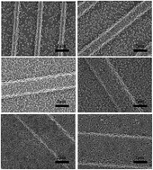
The investigation of surface morphology throughout layer deposition provides better insight into film growth process. The SEM images (see the ESI) show that the process began with small isolated grains that increased in size. Also noteworthy is that the nucleation of new particles was still continuing as time went on. The lack of conformal growth between the ZIF-8 islands reveals that the mechanism is Volmer–Weber, indicating the absorbate–absorbate interaction is greater than the absorbate–substrate interaction.46 Fig. 3 shows the topographical character of the ZIF-8 nanocrystals grown on sol–gel films patterned by soft-lithography. Surface-relief stripe-type microstructures with different widths and interspaces were used as masters for the replication of PDMS stamps. It is revealed that the surface coverage decreases as the period and width of the stripes decreases. Most of the ZIF-8 grains interconnect and a rather continuous surface can be obtained in the sample with stripe width of 5.3 μm and grating period (Λ) of 13.6 μm. But the situation is still worse than that grown on the pristine planar sol–gel film without microstructures (Fig. 2(b)). We also grew ZIF-8 on stripes with smaller periodicity. However, continuous ZIF-8 films cannot be obtained as the Λ was further reduced to 9.7 μm, 7.8 μm, 5.8 μm and 3.9 μm. The sample with the smallest Λ of 3.9 μm exhibit the lowest surface coverage. Sparse and separated grains can be distinctly identified.


image file: c5ra25794h-f3.tif
Fig. 3 SEM top views of ZIF-8 layer prepared on patterned sol–gel films after 1 cycle growth of 30 min with grating periods (Λ) of (a) 3.9 μm, (b) 5.8 μm, (c) 7.8 μm, (d) 9.7 μm, (e) 11.6 μm and (f) 13.6 μm.

Undoubtedly, more stripes were created per unit area and the area of side surface of the stripes increased at smaller periodicity. Considering the fact that all the sol–gel films were of the same chemical composition and experiencing the same 1 cycle growth procedure (30 min) at a constant temperature, one possible interpretation is that the corner of stripes would be favour of serving as nucleation sites. Once the nucleation events happen on the stripes and grains appear, the amount of accessible interspacing surface between grain boundaries for nucleation has decreased. Thus, continuous layer formation was prevented and the total coverage ratio was limited. It is straightforward that repeating the deposition cycles would help to accelerate surface coverage. Alternatively, the change of processing variables by increasing temperature and decreasing the reactant concentration would be useful, and also reduce surface roughness.46 It is reported that uniform, dense, and defect-free ZIF-8 ultrathin partly-crystalline nanofilms can be synthesized by a dip-coating approach. These findings might help us achieve complete surface coverage and solve roughness problem.47

In addition, the crystalline nature and identity of the ZIF-8 films were further confirmed by similarity of peak positions in the experimental XRD data of thin film and the corresponding ZIF-8 powder sample as depicted in Fig. 4(a). The ZIF-8 nanocrystal powder was prepared using the same reagents of Zn(NO3)2 and mIm dissolved in methanol.48 The XRD diffraction pattern for the ZIF-8 nanocrystalline layer grown on sol–gel film is essentially identical to that in the form of nanocrystal powder, apart from comparatively strong background due to the amorphous structure of sol–gel materials.


image file: c5ra25794h-f4.tif
Fig. 4 X-ray diffraction patterns of (a) ZIF-8 nanocrystalline layer grown on carboxylate-terminated sol–gel films and (b) ZIF-8 nanocrystal powder. POM photographs of the E7 filled VA cell observed with two different orientations of crossed polarizers, where the insets illustrate the structure of glass cell and the corresponding conoscopic images: (c) 0° and (d) 45°.

3.2 Vertical alignment of nematic LC E7 on ZIF-8 nanocrystalline film

The nematic LC E7 with positive dielectric anisotropy (no = 1.5330, ne = 1.7510), which was used to check the LC aligning ability of ZIF-8 films, is a mixture containing polar molecules (cyanobiphenyl and cyanoterphenol) at a specific composition. The molecular structures of each component are shown in Fig. 4(b). The POM photographs of E7 filled VA cell, which has a pair of ZIF-8 coated pristine sol–gel films, are presented in Fig. 4(c) and (d). Uniform dark state images were recorded when the sample is rotated arbitrarily. In addition, the conoscopic images of vertically aligned LCs were observed and shown along with the structure of ZIF-8 coated glass cell as the insets in Fig. 4(c). These results implied that E7 molecules are aligned perpendicularly to the ZIF-8 coated substrates.34,35

According to the empirical Friedel–Creagh–Kmetz (FCK) rule, vertical alignment can be achieved when γs < γLC, where γs describes the excess energy of the solid substrate and γLC is the strength of the LC–LC interaction.49 We propose a possible mechanism by which vertical alignment is introduced by ZIF-8: (1) the adhesion of the ZIF-8 on both substrates might mediate and lower the surface tension of the substrates, helping to foster a vertical LC alignment in which the elongated axis was normal to the substrate. (2) These arranged LCs on both inner surfaces guide and orient neighbouring LCs inside the VA cell. Therefore, the LCs between the ZIF-8 coated films were vertical aligned via strong van der Waals and weak molecules interactions directly or indirectly. The intermolecular force between the ZIF-8 and E7 is still unclear and we suspect it might be associated with the hydrophobic character of ZIF-8 and the polarity of E7 from another perspective.

3.3 HAN-LC prototype devices based on ZIF-8 aligning layer

As schematically shown in Fig. 5(a) and (b), two types of HAN cells were prepared with different inner surfaces on ITO substrates: Type A with different cell gaps of 8 μm, 10 μm and 12 μm, which has a rubbed homogenous PVA alignment layer facing a ZIF-8 coated pristine sol–gel film. Type B with cell gap of 8 μm, which has a rubbed PVA alignment layer which faces a ZIF-8 coated surface-relief sol–gel film. The rubbing direction is parallel to the grating stripes in Cell B. A disclination-free texture can be obtained after E7 infiltration. These glass cells were used to demonstrate the application of ZIF-8 coated pristine and microstructured films as voltage-dependent light modulator and switchable diffraction grating, respectively.
image file: c5ra25794h-f5.tif
Fig. 5 The schematic illustration of the HAN LC cells studied in this work. (a) Cell A, a rubbed homogenous PVA alignment layer facing a ZIF-8 coated pristine sol–gel film and (b) Cell B, a rubbed PVA alignment layer facing a ZIF-8 coated surface-relief sol–gel film. (c) Measured voltage-dependent optical transmittance curve of HAN cell for fixed input wavelength of 650 nm. (d) 0th and +/−1st order diffraction efficiency of the HAN grating (Λ = 13.6 μm) as a function of the applied AC (1 kHz) voltage.

The polarization of the probed beam makes an angle of 45° with respect to the rubbing direction. And the polarization of the analyzer is perpendicular to that of the probed beam. As shown in Fig. 5(c), for a conventional HAN cell (Type A) without surface-relief microstructures, there was no threshold in the electro-optical characteristics. It is in good agreement with the currently measured voltage-dependent optical transmittance.38 The curve oscillates with a maximum transmittance of ∼84% when applying 1.5 V AC voltage for the sample with cell gap of 8 μm. This transmittance value is comparatively high considering the multi-reflection induced by air/glass/LCs interfaces. It is notably the voltage required to obtain the maximum transmittance increases for samples with larger cell gaps of 10 μm and 12 μm as depict in the inset of Fig. 5(c). As we know, the shape of the electro-optical curve is in association with the modulation of phase retardation induced in the anisotropic HAN-LC cells. And the period of oscillation also extends as expected.

Switchable LC gratings were demonstrated as another kind of possible application by using E7 filled HAN LC grating cell (Type B). Fig. 5(d) plots 0th and +/−1st order diffraction efficiencies of the HAN LC grating. Grating period of 13.6 μm is chosen because it is proved that the ZIF-8 can be well grown to be almost interconnected and the vertical alignment of E7 is guaranteed at this scale. The shape of 0th order diffraction curve is similar to that of the voltage-dependent optical transmittance curve of the HAN cell (Type A). A maximum diffraction efficiency of ∼76% was recorded when applying the same 1.5 V AC voltage, slightly lower than the transmittance value in the HAN cell (Type A) because of the diffraction of a small fraction of the incident light into the +1st order and −1st order direction as depicted in the inset of Fig. 5(d). The diffraction is switchable and the voltage dependent diffraction behaviour of +1st and −1st orders is quite different because it is related to the change of the relative angle between the polarization axis of probed beam and the rubbing direction when the analyzer is cross-polarized with respect to the probed beam. In this case, the LCs actually play a passive role, as far as the main diffraction properties are dictated by the grating underneath.

It is known that the diffraction efficiency is mainly related to the duty cycle and refractive difference, etc. And obviously, the prototype grating structure proposed here is not optimized because the ZIF-8 layers were indiscriminately deposited on the whole underneath microstructured surface which dominate the diffraction behaviour. The purpose here is only to present the existence of diffraction in HAN cells with grating-stripe type microstructures. Theoretically, the diffraction efficiency and the tunability would be improved when the modulation capability of phase retardation between adjacent grating stripes was enhanced. It is reasonable to rationally design and alternate LC alignments to realize different types of LC phase grating, like HAN/PA or HAN/VA types, etc., in the future research.50,51

4. Conclusions

In summary, we characterized ZIF-8 nanocrystalline layer grown on carboxylate-terminated sol–gel films and reported its potential application as vertical alignment layer for nematic LC E7. It is revealed that the grating period of surface-relief microstructures patterned by soft lithography was crucial for the grown of high-quality interconnected MOFs layer. We also demonstrated the application as voltage-dependent light modulator and diffraction grating with dynamic switching behaviours. Toward the goal of incorporating metal–organic coordinated assemblies as smart interfaces, this research of employing ZIF-8 nanocrystalline film as LC vertical alignment layer might be imperative on the road to the development of optics-related multifunctional materials and devices, considering its tailorability and compatibility by selectively modification of functional groups on organic ligands.

Acknowledgements

This work was supported by the Fundamental Research Funds for the Central Universities (No. 20720140518), the Open Foundation Project of the State Key Lab of Silicon Materials (No. SKL2015-02) and National Natural Science Foundation of China (No. 61505173). The authors like to thank Prof. Shicheng Zhao and Dr Wenfei Zhang of East China University of Science and Technology for the contact angle measurements.

Notes and references

  1. S. S.-Y. Chui, S. M.-F. Lo, J. P. H. Charmant, A. G. Orpen and I. D. Williams, Science, 1999, 283, 1148–1150 CrossRef CAS PubMed.
  2. S. T. Meek, J. A. Greathouse and M. D. Allendorf, Adv. Mater., 2011, 23, 249–267 CrossRef CAS PubMed.
  3. B. Liu, J. Mater. Chem., 2012, 22, 10094–10101 RSC.
  4. L. E. Kreno, K. Leong, O. K. Farha, M. Allendorf, R. P. van Duyne and J. T. Hupp, Chem. Rev., 2011, 112, 1105–1125 CrossRef PubMed.
  5. K. S. Park, Z. Ni, A. P. Cote, J. Y. Choi, R. Huang, F. J. Uribe-Romo, H. K. Chae, M. O'Keeffe and O. M. Yaghi, Proc. Natl. Acad. Sci. U. S. A., 2006, 103, 10186–10191 CrossRef CAS PubMed.
  6. A. Demessence, C. Boissiere, D. Grosso, P. Horcajada, C. Serre, G. Ferey, G. J. A. A. Soler-Illia and C. Sanchez, J. Mater. Chem., 2010, 20, 7676–7681 RSC.
  7. G. Lu and J. T. Hupp, J. Am. Chem. Soc., 2010, 132, 7832–7833 CrossRef CAS PubMed.
  8. G. Lu, O. K. Farha, W. Zhang, F. Huo and J. T. Hupp, Adv. Mater., 2012, 24, 3970–3974 CrossRef CAS PubMed.
  9. S. Li, W. Shi, G. Lu, S. Li, S. C. J. Loo and F. Huo, Adv. Mater., 2012, 24, 5954–5958 CrossRef CAS PubMed.
  10. C. Hou, Q. Xu, J. Peng, Z. Ji and X. Hu, ChemPhysChem, 2013, 14, 140–144 CrossRef CAS PubMed.
  11. A. Betard and R. A. Fischer, Chem. Rev., 2011, 112, 1055–1083 CrossRef PubMed.
  12. D. Bradshaw, A. Garai and J. Huo, Chem. Soc. Rev., 2012, 41, 2344–2381 RSC.
  13. P. Falcaro, R. Ricco, C. M. Doherty, K. Liang, A. J. Hill and M. J. Styles, Chem. Soc. Rev., 2014, 43, 5513–5560 RSC.
  14. P. Falcaro, D. Buso, A. J. Hill and C. M. Doherty, Adv. Mater., 2012, 24, 3153–3168 CrossRef CAS PubMed.
  15. O. Shekhah, H. Wang, S. Kowarik, F. Schreiber, M. Paulus, M. Tolan, C. Sternemann, F. Evers, D. Zacher, R. A. Fischer and C. Woll, J. Am. Chem. Soc., 2007, 129, 15118–15119 CrossRef CAS PubMed.
  16. O. Shekhah, H. Wang, T. Strunskus, P. Cyganik, D. Zacher, R. Fischer and C. Woll, Langmuir, 2007, 23, 7440–7442 CrossRef CAS PubMed.
  17. D. Zacher, O. Shekhah, C. Woll and R. A. Fischer, Chem. Soc. Rev., 2009, 38, 1418–1429 RSC.
  18. R. Ameloot, E. Gobechiya, H. Uji-i, J. A. Martens, J. Hofkens, L. Alaerts, B. F. Sels and D. E. de Vos, Adv. Mater., 2010, 22, 2685–2688 CrossRef CAS PubMed.
  19. Y. Xiao, Y. Cui, Q. Zheng, S. Xiang, G. Qian and B. Chen, Chem. Commun., 2010, 46, 5503–5505 RSC.
  20. H. Xu, F. Liu, Y. Cui, B. Chen and G. Qian, Chem. Commun., 2011, 47, 3153–3155 RSC.
  21. Y. Cui, Y. Yue, G. Qian and B. Chen, Chem. Rev., 2012, 112, 1126–1162 CrossRef CAS PubMed.
  22. Y. Cui, H. Xu, Y. Yue, Z. Guo, J. Yu, Z. Chen, J. Gao, Y. Yang, G. Qian and B. Chen, J. Am. Chem. Soc., 2012, 134, 3979–3982 CrossRef CAS PubMed.
  23. H. Xu, X. Rao, J. Gao, J. Yu, Z. Wang, Z. Dou, Y. Cui, Y. Yang, B. Chenand and G. Qian, Chem. Commun., 2012, 48, 7377–7379 RSC.
  24. X. Rao, J. Cai, J. Yu, Y. He, C. Wu, W. Zhou, T. Yildirim, B. Chen and G. Qian, Chem. Commun., 2013, 49, 6719–6721 RSC.
  25. X. Rao, T. Song, J. Gao, Y. Cui, Y. Yang, C. Wu, B. Chen and G. Qian, J. Am. Chem. Soc., 2013, 135, 15559–15564 CrossRef CAS PubMed.
  26. Z. Dou, J. Yu, Y. Cui, Y. Yang, Z. Wang, D. Yang and G. Qian, J. Am. Chem. Soc., 2014, 136, 5527–5530 CrossRef CAS PubMed.
  27. Y. Zhou and B. Yan, J. Mater. Chem. C, 2015, 3, 8413–8418 RSC.
  28. G. Lu, O. K. Farha, L. E. Kreno, P. M. Schoenecker, K. S. Walton, R. P. van Duyne and J. T. Hupp, Adv. Mater., 2011, 23, 4449–4452 CrossRef CAS PubMed.
  29. Y. Wu, F. Li, W. Zhu, J. Cui, C. Tao, C. Lin, P. M. Hannam and G. Li, Angew. Chem., Int. Ed., 2011, 50, 12518–12522 CrossRef CAS PubMed.
  30. Y. Wu, F. Li, Y. Xu, W. Zhu, C. Tao, J. Cui and G. Li, Chem. Commun., 2011, 47, 10094–10096 RSC.
  31. F. M. Hinterholzinger, A. Ranft, J. M. Feckl, B. Ruhle, T. Beinand and B. V. Lotsch, J. Mater. Chem., 2012, 22, 10356–10362 RSC.
  32. J. Liu, E. Redel, S. Walheim, Z. Wang, V. Oberst, J. Liu, S. Heissler, A. Welle, M. Moosmann, T. Scherer, M. Bruns, H. Gliemann and C. Wöll, Chem. Mater., 2015, 27, 1991–1996 CrossRef CAS.
  33. W. Zhou, L. Lin, D. Zhao and L. Guo, J. Am. Chem. Soc., 2011, 133, 8389–8391 CrossRef CAS PubMed.
  34. S. Jeng, C. Kuo, H. Wang and C. Liao, Appl. Phys. Lett., 2007, 91, 061112 CrossRef.
  35. C. Kuo, S. Jeng, H. Wang and C. Liao, Appl. Phys. Lett., 2007, 91, 141103 CrossRef.
  36. B. Kinkead and T. Hegmann, J. Mater. Chem., 2010, 20, 448–458 RSC.
  37. H. Qi and T. Hegmann, ACS Appl. Mater. Interfaces, 2009, 1, 1731–1738 CAS.
  38. M. Chen, W. Chen, S. Jeng, S. Yang and Y. Chung, Opt. Express, 2013, 21, 29277–29282 CrossRef PubMed.
  39. C. Hong, T. T. Tang, C. Y. Hung, R. P. Pan and W. Fang, Nanotechnology, 2010, 21, 285201 CrossRef PubMed.
  40. X. Zhao, Y. Xia and G. M. Whitesides, J. Mater. Chem., 1997, 7, 1069–1074 RSC.
  41. D. Qin, Y. Xia and G. M Whitesides, Nat. Protoc., 2010, 5, 491–502 CrossRef CAS PubMed.
  42. S. R. Wasserman, Y. T. Tao and G. M. Whitesides, Langmuir, 1989, 5, 1074–1087 CrossRef CAS.
  43. D. Buso, K. M. Nairn, M. Gimona, A. J. Hilland and P. Falcaro, Chem. Mater., 2011, 23, 929–934 CrossRef CAS.
  44. A. U. Ortiz, A. P. Freitas, A. Boutin, A. H. Fuchs and F. Coudert, Phys. Chem. Chem. Phys., 2014, 16, 9940–9949 RSC.
  45. K. Zhang, R. P. Lively, C. Zhang, W. J. Koros and R. R. Chance, J. Phys. Chem. C, 2013, 117, 7214–7225 CAS.
  46. M. L. Ohnsorg, C. K. Beaudoin and M. E. Anderson, Langmuir, 2015, 31, 6114–6121 CrossRef CAS PubMed.
  47. J. Cookney, W. Ogieglo, P. Hrabanek, I. Vankelecom, V. Fila and N. E. Benes, Chem. Commun., 2014, 50, 11698–11700 RSC.
  48. J. Cravillon, S. Munzer, S. Lohmeier, A. Feldhoff, K. Huberand and M. Wiebcke, Chem. Mater., 2009, 21, 1410–1412 CrossRef CAS.
  49. S. Hwang, S. Jeng, C. Yang, C. Kuoand and C. Liao, J. Phys. D: Appl. Phys., 2009, 42, 025102 CrossRef.
  50. A. Y. Fuh, C. Huang, C. Liu, Y. Chen and K. Cheng, Opt. Express, 2011, 19, 11825–11831 CrossRef CAS PubMed.
  51. C. Yang, S. Li, W. Li, H. Zuo, L. Chen, B. Zhang and Z. Cai, Chin. Opt. Lett., 2015, 13(8)), 081603 CrossRef.

Footnote

Electronic supplementary information (ESI) available. See DOI: 10.1039/c5ra25794h

This journal is © The Royal Society of Chemistry 2016