
Facile formation of a hierarchical TiO2–SnO2 nanocomposite architecture for efficient dye-sensitized solar cells†
C. K. Lim*ab,
Y. Wanga and
L. Zhangb
aBiomedical Engineering and Materials Group, School of Engineering, Nanyang Polytechnic, 180 Ang Mo Kio Avenue 8, Singapore 569830
bTemasek Laboratories@NTU, Nanyang Technological University, 50 Nanyang Drive, Singapore 637553. E-mail: limc0105@e.ntu.edu.sg
First published on 1st March 2016
Abstract
In this paper, a hierarchical nanocomposite architecture consisting of TiO2 nanoflakes on SnO2 nanofibers was successfully synthesized using a simple and cost-effective hydrothermal method. The correlation between the structural changes in nanoflake size and density in accordance with the prolongation of hydrothermal growth duration was observed and discussed using high-resolution scanning and transmission electron microscopies. The dye-sensitized solar cells (DSSCs) utilizing these double-layered TiO2–SnO2 hierarchical nanostructures as photoelectrodes exhibited significant improvement in their photovoltaic properties. In particular, the DSSCs made from 24 h hydrothermally grown TiO2 nanoflakes on the surface of SnO2 nanofibers stood out to be the best performing cells, delivered a promising efficiency of 3.73%, which was more than a 4-fold increment over the DSSC with SnO2 nanofibers alone. This enhancement was attributed to the superiority in dye-loading and light scattering properties of the hierarchical architecture. Benefiting from the constituent advantages of both materials, the photoelectrodes with hierarchical nanostructures also inhibited back electron transfer to reduce electron recombination, leading to improved electron lifetime. These results suggest that a simple strategy to synthesize hierarchical nanostructures for efficient DSSCs was achieved.
1. Introduction
Since the introduction of low-cost, high-efficiency dye-sensitized solar cells (DSSCs) in 1991 by O'Regan and Grätzel, they have emerged as a potential alternative to conventional thin film solar cells.1 A typical DSSC consists of a few micrometer-thick nanocrystalline oxide covered with a monolayer of Ru dye, a redox electrolyte and a platinum counter electrode. So far, the conventional DSSCs using ruthenium- and porphyrin-based sensitizer have achieved respectable efficiencies of ∼11.0% and 13.0%, respectively.2–4 Recent breakthrough in the development of DSSC has been demonstrated using organic halide perovskite (e.g. CH3NH3PbX3, X = Br, I, Cl or their combinations) as photosensitizer whereby the power conversion efficiency of over 15.0% was achieved.5 Over the past two decades, significant research efforts have been devoted on the various components of DSSC to further improve the energy conversion efficiency. While metal complexes and organic dyes are widely developed, natural and vegetable dyes as sensitizer for DSSC are also gaining more attentions due to their “environmental friendly” characteristics while producing promising photovoltaic efficiency ∼2.7%.6–8 Extensive research activities have been carried out as well to replace the liquid electrolytes in DSSC into solid-state or quasi solid-state electrolytes in order to enhance the stability and efficiency of DSSC.9–11 New counter electrode materials utilizing carbon-based nanomaterials have also been investigated and applied in DSSC as alternative to Pt-coated FTO glasses to improve the charge transfer properties.4,12,13 The choice and the architecture of wide band gap oxide semiconductor is also an interesting research topic that has been extensively studied to improve the conversion efficiency of DSSC.14,15 The mesoporous semiconductor oxide layer deposited on the transparent conducting oxide (TCO) glass substrate as the photoelectrode, is an essential constituent structure of the DSSC in separating and transferring the photo-generated electrons in the dye sensitizer towards the collection electrode. Currently, TiO2 is the favored metal oxide for DSSCs. Several alternative oxide semiconductor materials such as ZnO,16,17 SnO2,18,19 SrTiO3,20 Nb2O5 21 and BaSnO3 22 have been investigated for their potential in substituting the TiO2 as photoelectrode. Among them, SnO2 stands out to be a potential candidate for DSSCs.One of the key advantages of SnO2 over TiO2 is that SnO2 offers higher electron mobility (100 to 200 cm2 V−1 s−1) which can be translated into faster transport of photo-injected electrons for collection.23 Other than that, SnO2 also possesses wider band gap (3.6 eV) than anatase TiO2 (3.2 eV), which creates less oxidative holes in the valence band under UV illumination to minimize the dye degradation rate and improve the long-term stability of DSSCs.24 However, the use of SnO2 is also limited by a few drawbacks. The inferior performance of the DSSCs with SnO2 photoelectrode has been attributed to higher electron recombination rate due to the 300 mV positive shift of the conduction-band edge of SnO2 with respect to TiO2.25 Other than that, the lower isoelectric point also leads to poorer dye loading.26 The rate of electron injection from the sensitizer to the conduction band of SnO2 was also found to be also much slower as compared to TiO2.27 As proposed by Goodenough and co-workers, the dehydrative coupling of carboxylic acid groups with surface TiO2 formed ester-type linkages.28 The π* orbitals of the dcb ligand would promote rapid excited-state electron injection into the conduction band of TiO2, which mainly composed of unfilled d orbitals. On the other hand, the SnO2 possesses predominantly s-orbital character. The Sn s orbitals are orthogonal to the carboxylate π system resulting in less favorable orbital mixing.29 Hence, the electron injection rates into conduction band of SnO2 are not as efficient as TiO2. These issues have been addressed by incorporating a core–shell structure with interfacial layers of wide band gap oxides, such as TiO2,30–32 MgO33,34 or Al2O3 35 in between the SnO2 and dye sensitizer. By using this core–shell system, a better charge separation has been achieved by suppressing charge recombination in the coupled oxide semiconductors system with different energy levels.
The development of one-dimensional (1D) metal–oxide architectures have also been explored for DSSCs to overcome the poor interconnectivity in between the nanoparticles that resulted in high charge recombination losses.36,37 These ordered nanomaterials have contributed to faster electron transport and slower charge recombination in DSSCs. One simple and versatile technique for producing continuous ultrafine nanofibers in nanometer scale diameter is through electrospinning.38–40 Electrospinning of 1D polycrystalline SnO2 nanomaterials with extremely high aspect ratios and specific surface areas have been reported and investigated in many functional applications such as solar cells,41 photocatalysis,42,43 batteries44 and gas sensor.45,46
In this work, we propose a simple approach to revamp 1D SnO2 nanofibers to three-dimensional (3D) hierarchical TiO2–SnO2 nano-architecture. This redefined core–shell nanostructure was achieved by hydrothermally growth of TiO2 nanoflakes for different durations on the SnO2 nanofibers. Then, the resulting TiO2–SnO2 hierarchical heterostructures were characterized and fabricated into the photoelectrode for DSSCs. To study the effects of these double-layered TiO2–SnO2 hierarchical heterostructures as photoelectrode, the photovoltaic properties of these DSSCs were investigated in details.
2. Experimental
2.1 Electrospinning of SnO2 nanofibers
A solvent containing 22 g of ethanol and 22 g of N,N-dimethyl formamide (DMF) were mixed together using magnetic stirring for 1 h at room temperature. Then, 2.67 g of tin(II) chloride dihydrate (SnCl2·2H2O) was added into the mixed solvent under stirring condition until it was completely dissolved. Subsequently, 4 g of polyvinyl pyrrolidone (PVP, Mw = 1![[thin space (1/6-em)]](https://www.rsc.org/images/entities/char_2009.gif) 300000 g mol−1) was added into the resulting solution under vigorous stirring for 2 h at room temperature to form a homogenized viscous precursor. The as-prepared precursor solution was then transferred into a plastic syringe for electrospinning. The electrospinning solution was fed at a speed of 1.5 ml h−1. The voltage applied to the tip was 20 kV and the distance between the needle tip and the collector plate was 10 cm. During the electrospinning process, the solution on the tip of the needle was ejected under strong electric field to form a dense fiber membrane on a collector of aluminium foil. Then, the fiber membrane was manually peeled off from the aluminium foil and calcinated at 500 °C for 2 h with a heating rate of 1.0 °C min−1 to remove the PVP content. Finally, the electrospun SnO2 nanofibers were obtained.
300000 g mol−1) was added into the resulting solution under vigorous stirring for 2 h at room temperature to form a homogenized viscous precursor. The as-prepared precursor solution was then transferred into a plastic syringe for electrospinning. The electrospinning solution was fed at a speed of 1.5 ml h−1. The voltage applied to the tip was 20 kV and the distance between the needle tip and the collector plate was 10 cm. During the electrospinning process, the solution on the tip of the needle was ejected under strong electric field to form a dense fiber membrane on a collector of aluminium foil. Then, the fiber membrane was manually peeled off from the aluminium foil and calcinated at 500 °C for 2 h with a heating rate of 1.0 °C min−1 to remove the PVP content. Finally, the electrospun SnO2 nanofibers were obtained.
2.2 Preparation of SnO2 nanofiber photoelectrodes
The electrospun SnO2 nanofibers were firstly dispersed in ethanol using stirring and ultrasonication to form a homogenized colloidal. Next, this homogenized colloidal was poured into the beaker containing 10 wt% ethyl cellulose (Aldrich) in ethanol prepared earlier. Finally, alpha-terpineol (97%, Aldrich) was added into the colloidal and stirred. The colloidal was then heated up to 80 °C under stirring on a hotplate to evaporate the ethanol content. Finally, a thick homogenized paste was formed and it was deposited on the FTO glass using doctor blade method. The as prepared photoelectrodes made of SnO2 nanofibers were subjected to annealing at 450 °C in air for 30 minutes.2.3 Synthesis of TiO2–SnO2 hierarchical nanostructures
The TiO2–SnO2 hierarchical nanostructures were grown using hydrothermal method. First, 0.1 ml of titanium isopropoxide (TTIP, 97%, Aldrich) was added to 50 ml of a 0.45 M hydrochloric acid solution under vigorous stirring at room temperature for 2 h until a clear solution was obtained. Then, the solution was transferred to a Teflon vessel. The SnO2 nanofibers and photoelectrodes prepared earlier were immersed into solution in the Teflon vessel. Then, the vessel was placed into the stainless steel autoclave for hydrothermal growth at temperature 95 °C for 3, 7, 15 and 24 hours respectively. After the hydrothermal process, the nanofibers and photoelectrodes were taken out and rinsed thoroughly with DI water. The photoelectrodes with mesoporous TiO2–SnO2 hierarchical nanostructures from different growth durations were ready for use.2.4 Fabrication of DSSC
The photoelectrodes with mesoporous TiO2–SnO2 hierarchical nanostructures were soaked in 40 mM TiCl4 (99%, Merck) solution at 70 °C for 30 minutes, followed by annealing at 450 °C for 30 minutes in air. Next, the freshly-annealed photoelectrodes were dipped into the 0.25 mM N719 dye solution (Solaronix) for overnight. The platinum coated counter electrode was then clamped onto the photoelectrode, with the Surlyn spacer (30 μm) in between. Finally, the iodide electrolyte (Solaronix, Iodolyte AN50) was filled through capillary action in vacuum condition to allow the complete infiltration of electrolyte into the mesoporous layer. The DSSCs prepared were ready for photovoltaic testing. A total of five different types of photoelectrodes made from pristine SnO2 nanofibers (sample SS) and composites TiO2–SnO2 hierarchical nanostructures grown at different hydrothermal durations (3 h for sample TS03, 7 h for sample TS07, 15 h for sample TS15 and 24 h for sample TS24) were prepared for investigation.2.5 Characterizations
The crystallography of the electrospun SnO2 fiber and hierarchical nanostructures TiO2 on SnO2 nanofibers were studied using X-ray diffraction (XRD) measurements. The XRD patterns were recorded at room temperature using Pan Analytical X'Pert Pro MPD X-ray diffractometer with Cu K-alpha radiation (λ = 1.5406 Å) operating at 40 kV and 40 mA. The surface morphologies of the nanofibers were observed using field emission scanning electron microscope (FESEM, JEOL-JSM-6701F) and Field Emission Transmission Electron Microscopy (TEM, JEOL-JEM 2010F). The PerkinElmer Lambda 950 UV/Vis/NIR spectrophotometer system was used to determine the amount of dye adsorbed onto the photoelectrode. The dye desorption was carried out in a mixed solution of water and ethanol containing 0.1 M NaOH. The current–voltage (I–V) curves of the solar cells were measured under simulated solar light irradiation with intensity of 100 mW cm−2. Electrochemical Impedance measurements were carried out using Metrohm Autolab system in the frequency range of 1 mHz to 1000 kHz at room temperature, illuminated under solar light with intensity of 100 mW cm−2. The applied bias was set to be the open circuit potential of the DSSC and the ac amplitude was 10 mV.3. Results and discussion
3.1 Material characterizations
The phase purity and crystal structure of the as-electrospun SnO2 nanofibers and the hydrothermal growth of TiO2–SnO2 hierarchical heterostructures for different durations were determined by XRD, as shown in Fig. 1. After the annealing at 500 °C for 2 h, all the peaks in the XRD patterns for SnO2 nanofibers were indexed accordingly for the cassiterite phase (space group P42/mnm) of SnO2 (JCPDS file 41-1445). No impurity or secondary phase could be detected in the XRD pattern of SnO2 nanofibers. The as-synthesized SnO2 nanofibers were polycrystalline and the crystalline particle size was estimated by using the Scherrer equation, D = 0.9λ/β(cosθ), where λ is the wavelength of the X-ray (1.54 Å), β is the full-width at half-maximum (FWHM) in radians, and θ is the Bragg angle in the diffraction pattern. Using this equation, the mean crystalline particle size was estimated to be 13.9 nm.
 | ||
| Fig. 1 XRD patterns of SnO2 nanofibers and TiO2–SnO2 hierarchical heterostructures hydrothermally grown at different durations (3, 7, 15 and 24 h). | ||
Compared with the pristine SnO2 nanofibers, additional XRD characteristic peaks of rutile TiO2 could be observed for the case of composite TiO2–SnO2 hierarchical heterostructures. The co-existence of the tetragonal SnO2 and TiO2 phases has confirmed that the formation of bilayered hierarchical structure with TiO2 nanocrystallites grown on the surface of SnO2 nanofibers through the facile single-step hydrothermal process. There was no other diffraction peak indicating the formation of any new composite. With the prolonged growth duration from 3 h to 24 h, the overall peak intensity of the TiO2 became more prominent, resulted in the peak intensity of SnO2 to be partially screened off. This suggests that the presence and growing amount of TiO2 nanostructures formed on top of the surfaces of SnO2 nanofibers. Increasing the hydrothermal growth duration has also contributed to larger average sizes of TiO2 nanocrystallites sizes as calculated based on the Scherrer equation (ESI S1†).
The morphologies of the electrospun SnO2 nanofibers and the corresponding TiO2–SnO2 hierarchical heterostructures were investigated by FESEM. Fig. 2a presents the FESEM images of electrospun SnO2 nanofibers after annealed at 500 °C in air for 2 h. The SnO2 nanofibers were randomly oriented with rough porous structure after the PVP was completely decomposed (ESI S2†). The size of SnO2 nanofibers was around 150–200 nm in diameter and lengths could reach up to a few tens of micrometers. Observation at higher magnification as shown in Fig. 2a(ii) reveals that the nanofibers were formed by SnO2 nanoparticles that were densely packed together to create a long and compact fibrous structure. The rough surface of SnO2 nanofibers is beneficial for high amount of adsorption of dye molecules.
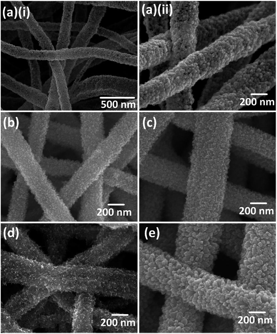 | ||
| Fig. 2 SEM images of TiO2–SnO2 hierarchical heterostructures hydrothermally grown at different durations. (a-i/ii) Pristine SnO2 nanofibers at different magnifications; (b) 3 h; (c) 7 h; (d) 15 h; (e) 24 h. | ||
The FESEM images in Fig. 2b–e reveal that the time dependent study (3, 7, 15, 24 h) of hierarchical nano-architecture formed by TiO2 nanoflakes hydrothermally grown on the SnO2 nanofibers. The length of these hierarchical nano-architectures maintained at several tens of micrometers (ESI S3†). This shows that the incorporation of TiO2 nanoflakes using hydrothermal method did not destroy the tubular nanofibers structure. In this case, the TiO2 nanoflakes were evenly distributed to form a uniform coating along the length of nanofibers. Hence, the SnO2 nanofibers can be regarded as the basic matrix for the TiO2 nanoflakes to grow and form the composite hierarchical nanostructures. In the initial 3 and 7 h growth as shown in Fig. 2b and c, tiny TiO2 nanoflakes nucleated on the surfaces of SnO2 nanofibers. Further prolongation of the hydrothermal growth to 15 h (Fig. 2d) resulted in the enhancement of filling rate between the adjacent SnO2 nanoparticles and the TiO2 nanoflakes to form a densely populated nanoflakes network. Finally, when the hydrothermal growth duration was extended to 24 h, numerous TiO2 nanoflakes started to evolve into this prominent hierarchical nano-architecture as revealed in Fig. 2e. The average diameter of these nanofibers has also increased noticeably. In short, a hierarchical heterostructures composed of large amount of TiO2 nanoflakes arrays on SnO2 nanofibers were successfully achieved using this facile one-step hydrothermal process.
The morphology and crystallinity of SnO2 nanofibers and TiO2 nanoflakes were further investigated in details using TEM. Fig. 3a depicts a TEM of an individual SnO2 nanofiber with the tube-shaped structure with hollow core and a wall thickness of about 20 nm. The nanotubes consisted of bonded nanoparticles with an average size of around 20 nm. Many nanopores were observed within the spaces between adjacent SnO2 nanoparticles which could be due to the decomposition of PVP. The high resolution TEM (HRTEM) image in Fig. 3a(iii) shows well resolved lattice fringes, signifying that the SnO2 nanoparticle in the nanotube possessed excellent crystallinity. The lattice fringes with the d spacing of 0.264 nm corresponds to the (101) plane of tetragonal SnO2. The ring-shaped selected area electron diffraction (SAED) pattern (inset of Fig. 3a(iii)) indicates that the SnO2 nanofibers were polycrystalline, in good accordance with the XRD data described above.
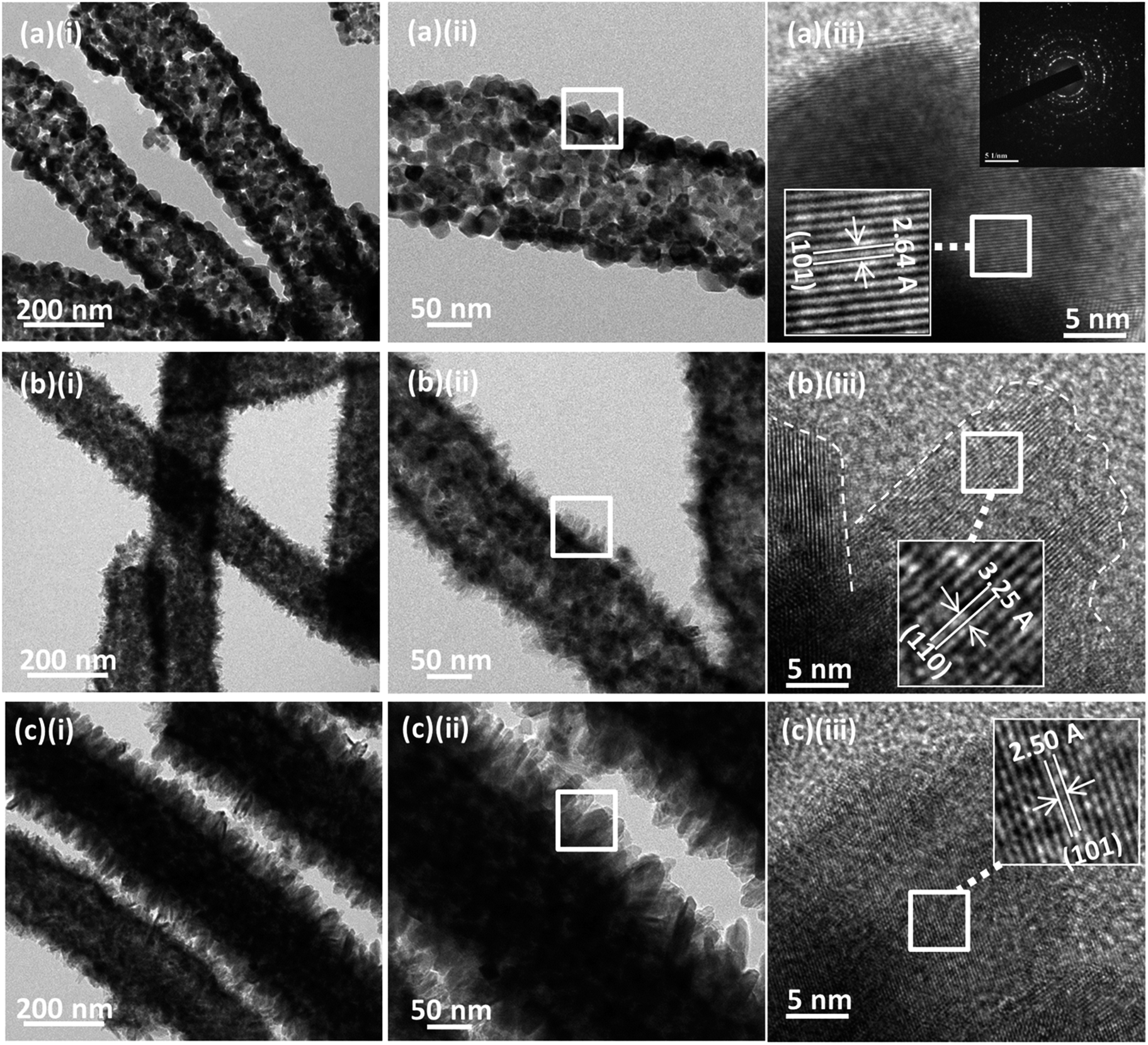 | ||
| Fig. 3 (a) TEM and HRTEM images of SnO2 nanofibers. The inset in (a-iii) is the SAED patterns reveal the crystallinity of SnO2. Selected TiO2–SnO2 hierarchical heterostructures hydrothermally grown at different durations; (b) 7 h; (c) 24 h. | ||
Fig. 3b and c further illustrates the hierarchical TiO2 nano-architecture arrays constituted by an assembly of multi-scale nanoflakes based on 7 and 24 h of growth duration. The TEM observations coincide well with the FESEM images shown earlier. These sequential images reveal a morphological and structural transformation from pristine SnO2 nanofibers to TiO2–SnO2 hierarchical nanostructures. With SnO2 nanofibers as the building block, the TiO2 nanoflakes started to germinate and form the tiny branch-like nanostructures surrounding the entire nanofibers after 7 h of growth duration. With increased hydrothermal growth duration, higher surface coverage density was achieved and the structure of the nanoflakes becomes more prominent. Extending the hydrothermal growth duration to 24 h resulted in prominent TiO2 nanoflakes that were compactly developed on the surfaces of SnO2 nanofibers. The length of the nanoflakes could reach up to around 50 nm (Fig. 3c(ii)). The clear lattice fringes of the TiO2 nanoflakes were observed from the HRTEM images. The interplanar spacing obtained from the lattice fringes along d (110) was 0.325 nm, which could be assigned to the rutile TiO2 (110). The lattice constant spacing with 0.250 nm pertained to the d-spacing of rutile TiO2 (101) crystal planes. These results confirmed that the hierarchical heterostructures with TiO2 nanoflakes on SnO2 nanofibers were well created.
The successfully growth of TiO2 nanoflakes onto the surface of SnO2 nanofibers can be explained by the recrystallization process which involved the dissolve and grow method.32,33 During the hydrothermal growth process, The Ti species from TTIP precursor reacts with concentrated acidic solution to form TiCl3. The Ti3+ species formed are not stable. Hence, it will immediately react with water to form TiOH2+. Finally, the TiOH2+ is oxidized into Ti(IV) from the reaction with dissolved oxygen. These Ti(IV) complex ions act as the growth units to form nanostructures. The overall growth process can be described as follow:
| 2Ti + 6HCl → 2TiCl3 + H2O | (1) |
| Ti3+ + H2O → TiOH2+ + H+ | (2) |
| TiOH2+ + O2 → Ti(IV)-oxo species + O2− → TiO2 | (3) |
3.2 Photovoltaic performance
The hierarchical TiO2–SnO2 nanostructures were fabricated into the photoelectrode for DSSCs. A total of five DSSCs based on SnO2 nanofibers and TiO2–SnO2 hierarchical nanostructures as photoelectrode were fabricated for study. Fig. 4 depicts photovoltaic performance of DSSC with hydrothermal growth of TiO2 nanoflakes/SnO2 nanofibers. The corresponding photovoltaic parameters such as short-circuit current density (JSC), open-circuit voltage (VOC), fill factor (FF), and conversion efficiency (η) derived from the photocurrent density–voltage (J–V) curves were summarized in Table 1. | ||
| Fig. 4 (a) Photovoltaic J–V curves for DSSCs with TiO2–SnO2 hierarchical heterostructures grown at different durations. (b) Dark current measurements. | ||
| Samples | VOC (V) | JSC (mA cm−2) | FF (%) | η (%) |
|---|---|---|---|---|
| SS | 0.38 | 6.50 | 34.0 | 0.84 |
| TS03 | 0.51 | 8.35 | 40.1 | 1.70 |
| TS07 | 0.59 | 8.30 | 42.6 | 2.08 |
| TS15 | 0.60 | 11.65 | 46.9 | 3.28 |
| TS24 | 0.61 | 12.68 | 48.5 | 3.73 |
The DSSC with pristine SnO2 nanofibers as photoelectrode (sample SS) showed very poor photovoltaic performance, with the overall power conversion efficiency of less than 1.0%. As mentioned previously, this result can be attributed to the lower electron trapping density of SnO2, which has been reported to be the key in retarding interfacial charge recombination dynamics in DSSC.13 Consequently, the high interfacial charge recombination resulted in low VOC by decreasing the concentration of electrons in the conduction band of the semiconductor. With reduced forward injection current, the JSC value was also limited.47,48
By utilizing the TiO2–SnO2 hierarchical nanostructures as photoelectrode, the conversion efficiencies of the DSSCs improved drastically. The best cell (sample TS24) delivered a conversion efficiency of 3.73%, demonstrated more than 4-fold improvement over the DSSC with pristine SnO2 nanofibers as photoelectrode. Noticeable increments in the photovoltaic parameters were also observed. The improvement in the VOC value can be explained from the formation of this double-layered TiO2–SnO2 structure that creates a surface dipole layer that is dependent on the isoelectric point of the materials involved.49,50 The isoelectric point of TiO2 is higher than SnO2 and hence it yields a surface dipole layer towards the SnO2. This dipole layer might shift the conduction band of SnO2 to a more negative value, causing an increase in VOC. The prominent increases in JSC and FF also indicate that the interfacial charge recombination on SnO2 electrodes were effectively suppressed by applying the TiO2 nanoflakes on the SnO2 nanofibers. The dark current measurement as shown in Fig. 4b was also carried out to investigate effectiveness of TiO2–SnO2 system for achieving high efficiency DSSC. The dark current can be used to represent the charge recombination between the electrons in photoelectrode and I3− ions in electrolyte.51 Owing to lower conduction band energy level for SnO2 than TiO2, the SnO2 establishes an expressway between TiO2 and FTO glass to promote the transport of the photogenerated electrons. At the same time, the TiO2 also acts as a barrier to effectively reduce the recombination of photogenerated electrons in anode and I3− ions in. As such, the dark currents for the TS-based solar cells were generally lower than the sample SS, which in turn improved the overall photovoltaic performance.
The sequential improvement of photovoltaic performance according to the growth duration of TiO2 nanoflakes is explained as follows. In the first 3 and 7 h of growth, some back electron transfer from uncovered areas of SnO2 nanofibers still existed. Hence, the improvement in the photovoltaic performances for sample TS03 and TS07 were relatively minor. When the hydrothermal growth duration was extended to 24 h, prominent TiO2 nanoflakes formed densely on the surface of SnO2 nanofiber to produce the hierarchical nano-architecture. This has greatly enhanced the coverage density to inhibit the back electron transfer and increased the surface area for dye loading. The dye-desorptions on these photoelectrodes were performed and the amount of dye absorbed onto the surface of TiO2–SnO2 hierarchical heterostructures (sample TS24, 2.9 × 10⁻⁷ mol cm−2) was found to be 61.1% greater than the pristine SnO2 nanofibers (sample SS, 1.8 × 10⁻⁷ mol cm−2) (ESI S5†). The enhancement in the dye-loading as a result of increased specific surface area of the photoelectrode made from TiO2–SnO2 hierarchical nanostructures has directly contributed to higher JSC.
In addition to higher dye loading capability, the hierarchical TiO2–SnO2 photoelectrode also appeared to possess enhanced light scattering ability. Enhanced light scattering ability of a photoelectrode is crucial for high light harvesting efficiency that contributes to higher photocurrent density of a DSSC.52–54 The difference in the architecture of photoelectrode has a direct influence on the light scattering property of a DSSC.55,56 As clearly perceived from the diffuse reflectance spectra of sample TS24 and SS in Fig. 5, the hierarchical TiO2–SnO2 film has higher diffuse reflection ability in the wavelength range from 430 nm to 800 nm. This suggests that the film possessed supreme light scattering capability, which allowed multiple light traveling paths to improve the light interactions with the dye-molecules anchored on the surface of the metal oxide. In contrast, the SnO2 nanofiber film demonstrated comparatively poorer light scattering capability. This has resulted in the unabsorbed light to penetrate through the film with limited back-scattered light for multiple interactions. Hence, the light harvesting efficiency and photocurrent were relatively poor.
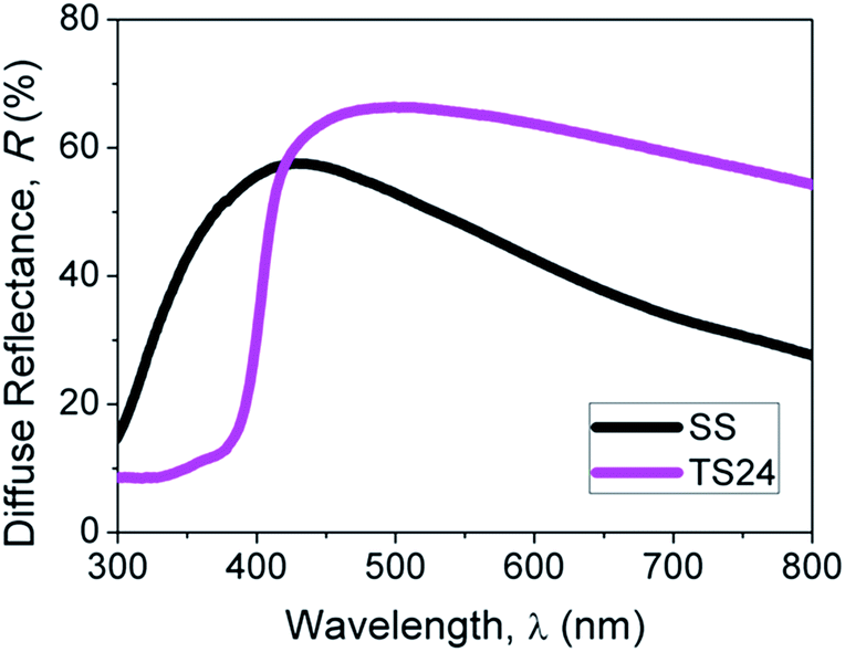 | ||
| Fig. 5 Comparison of diffuse reflectance spectra for SnO2 nanofiber film and hierarchical TiO2–SnO2 nanocomposite film. | ||
EIS has been widely employed to investigate the kinetics of electrochemical and photoelectrochemical system. It has been used to study the prominent electronic and ionic processes in DSSCs.57,58 To distinguish the difference in the interfacial characteristics of these photoelectrodes, the EIS spectra of the DSSCs were measured at an applied bias of VOC and a frequency range from 0.1 Hz to 100 kHz, with ac amplitude of 10 mV in a simulated solar light. Fig. 6 shows EIS spectra of the DSSCs with the photoelectrode made from SnO2 nanofiber and hierarchical TiO2–SnO2, respectively. In general, 3 semicircles in the order of increasing frequency can be observed from the Nyquist plot. The low frequency region is attributed to the Nernst diffusion within the electrolyte, while the intermediate frequency features the electron transport in the oxide semiconductor/dye/electrolyte interface. Lastly, the high frequency peak corresponds to the charge transfer at the platinum coated counter electrode. The equivalent circuit diagrams were fitted based on the general transmission line model for DSSCs as shown in the inset of Fig. 6a.
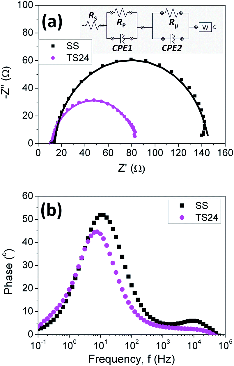 | ||
| Fig. 6 (a) Nyquist plot of DSSCs with SnO2 nanofibers and hierarchical TiO2–SnO2 heterostructures as photoelectrode under simulated sunlight illumination. Inset shows the equivalent circuit diagram. (b) Corresponding Bode phase plot. | ||
Since the EIS measurements were carried out at open-circuit potential bias, there was no current passing through the external circuit. The photogenerated electrons injected from the dye molecules into the oxide semiconductor must be recombined by I3− ions at this interface. Hence, the Rμ resistance shown in the Nyquist plot represents a net charge-transfer resistance at the oxide semiconductor/dye/electrolyte interface. With higher dye-loading for sample TS24, more photogenerated electrons were injected into the oxide semiconductor under illumination. Consequently, the net charge-transfer resistance at this interface was much lower for sample TS24 as compared to sample SS.
The lifetime of photogenerated electrons in the oxide film (tr) can be estimated from the maximum angular frequency (ωmax) of the impedance semicircle arc at middle frequencies, according to the relation tr = 1/ωmax = 1/2πfmax, where fmax is the maximum frequency of the mid-frequency peak.59 As shown in the inset of Fig. 6b, the fmax value for sample TS24 is 7.14 Hz (tr-TS24 = 22.3 ms), much lower than the values for sample SS at 10.99 Hz (tr-SS = 14.5 ms). These data suggest that photogenerated electrons in the hierarchical TiO2–SnO2 film have a longer lifetime than in SnO2 nanofiber film. This increment in the tr value corresponds to the effective retardation of charge recombination reaction between photoinjected electrons with I3− during the electron transport through the film made with hierarchical TiO2–SnO2 composite.
Although SnO2 is always considered as a potential material for photoelectrode, the DSSC with SnO2 photoelectrodes generally shows lower conversion efficiency as compared to its TiO2 counterpart due to its inherently larger charge recombination, slower charge injection and poorer dye-loading. This study has demonstrated that proper design of SnO2 photoelectrodes can be used to alleviate these issues. The hierarchical nanostructure of TiO2–SnO2 employed for DSSC has led to improved photovoltaic performance with respect to those based on pristine SnO2 nanofiber. The proposed architecture is efficient for DSSC with SnO2 photoelectrode due to the larger surface area for dye-loading, inhibition of back-electron transfer, better carrier lifetime and enhanced light scattering effects.
However, the improved conversion efficiency is still inferior with reference to the state of the art DSSC. The overall low conversion efficiency might be attributed to lower dye-loading in these photoelectrodes deposited in this work, in contrast to a typical DSSC with densely packed nanoparticles film. The thicknesses of the SnO2 layer used in this study were controlled to be around ∼6 μm for better consistency. It is believed that increasing the thickness of SnO2 layer can improve the overall dye-loading to further enhance the short circuit current density. Besides that, large pores between the nanofibers could be observed from the SEM images. This has caused a less compact structure and affected the dye-loading and thus the overall efficiency.
4. Conclusions
In summary, the hierarchical hybrid architecture with TiO2 nanoflakes on SnO2 nanofibers has been successfully developed by combining the electrospinning and single-step hydrothermal growth method. The high-surface to volume ratio of this hierarchical hybrid nanostructure, along with the appropriate combination of materials, makes it an excellent candidate for photoelectrode in DSSC. In general, the DSSC made using hierarchical hybrid nanostructure of TiO2–SnO2 demonstrated improved photovoltaic performance compared to those based on pristine SnO2 nanofiber. As the hydrothermal growth duration increases, the makeover of tubular structure of SnO2 nanofiber to hierarchical hybrid architecture of TiO2–SnO2 was successfully achieved, leading to higher specific surface area. The back electron transfer for recombination in this hierarchical hybrid structure has been successfully retarded. Consequently, the lifetime of the photogenerated electron transported through the hierarchical matrix was improved. The synergistic effects from all these factors, together with the excellent light scattering ability have contributed to extraordinary improvement of photocurrent density, open circuit potential and the fill factor of the DSSC. These improvements have in turn transformed into a remarkable 4-fold improvement in the photovoltaic power conversion efficiency of the DSSC made from the well-defined TiO2 nanoflakes on SnO2 nanofibers hydrothermally grown for 24 h. This work suggests that this novel hierarchical nanostructure synthesized through this facile method may serve as a new generation photoelectrode for high efficiency DSSC. On top of that, its potential applications are foreseeable to be extended and implemented in other fields such as photocatalysis and charge storage.References
- B. O'Regan and M. Grätzel, Nature, 1991, 353, 737–740 CrossRef.
- M. K. Nazeeruddin, S. M. Zakeeruddin, R. Humphry-Baker, M. Jirousek, P. Liska, N. Vlachopoulos, V. Shklover, C.-H. Fischer and M. Grätzel, Inorg. Chem., 1999, 38, 6298–6305 CrossRef CAS PubMed.
- C.-Y. Chen, M. Wang, J.-Y. Li, N. Pootrakulchote, L. Alibabaei, C.-h. Ngoc-le, J.-D. Decoppet, J.-H. Tsai, C. Grätzel, C.-G. Wu, S. M. Zakeeruddin and M. Grätzel, ACS Nano, 2009, 3, 3103–3109 CrossRef CAS PubMed.
- S. Mathew, A. Yella, P. Gao, R. Humphry-Baker, F. E. CurchodBasile, N. Ashari-Astani, I. Tavernelli, U. Rothlisberger, K. NazeeruddinMd and M. Grätzel, Nat. Chem., 2014, 6, 242–247 CrossRef CAS PubMed.
- M. Liu, M. B. Johnston and H. J. Snaith, Nature, 2013, 501, 395–398 CrossRef CAS PubMed.
- G. Calogero, A. Bartolotta, G. di Marco, A. di Carlo and F. Bonaccorso, Chem. Soc. Rev., 2015, 44, 3244–3294 RSC.
- G. Calogero, J. H. Yum, A. Sinopoli, G. di Marco, M. Grätzel and M. K. Nazeeruddin, Sol. Energy, 2012, 86, 1563–1575 CrossRef CAS.
- C. Sandquist and J. L. McHale, J. Photochem. Photobiol., A, 2011, 221, 90–97 CrossRef CAS.
- L. Y. Chang, C. P. Lee, C. T. Li, M. H. Yeh, K. C. Ho and J. J. Lin, J. Mater. Chem. A, 2014, 2, 20814–20822 CAS.
- J. Burschka, A. Dualeh, F. Kessler, E. Baranoff, N. L. Cevey-Ha, C. Yi, M. K. Nazeeruddin and M. Grätzel, J. Am. Chem. Soc., 2011, 133, 18042–18045 CrossRef CAS PubMed.
- I. Chung, B. Lee, J. He, R. P. H. Chang and M. G. Kanatzidis, Nature, 2012, 485, 486–489 CrossRef CAS PubMed.
- M. J. Ju, I. Y. Jeon, J. C. Kim, K. Lim, H. J. Choi, S. M. Jung, I. T. Choi, Y. K. Eom, Y. J. Kwon, J. Ko, J. J. Lee, H. K. Kim and J. B. Baek, Adv. Mater., 2014, 26, 3055–3062 CrossRef CAS PubMed.
- G. Calogero, F. Bonaccorso, O. M. Marago, P. G. Gucciardi and G. di Marco, Dalton Trans., 2010, 39, 2903–2909 RSC.
- J. Liu, T. Luo, S. Mouli, F. Meng, B. Sun and M. Li, Chem. Commun., 2010, 46, 472–474 RSC.
- H. Sun, J. Deng, L. Qiu, X. Fang and H. Peng, Energy Environ. Sci., 2015, 8, 1139–1159 CAS.
- S. Zhu, L. Shan, X. Chen, L. He, J. Chen, M. Jiang, X. Xie and Z. Zhou, RSC Adv., 2013, 3, 2910–2916 RSC.
- L.-Y. Chen and Y.-T. Yin, Nanoscale, 2013, 5, 1777–1780 RSC.
- H. J. Snaith and C. Ducati, Nano Lett., 2010, 10, 1259–1265 CrossRef CAS PubMed.
- A. Birkel, Y. G. Lee, D. Koll, X. V. Meerbeek, S. Frank, M. J. Choi, Y. S. Kang, K. Char and W. Tremel, Energy Environ. Sci., 2012, 5, 5392–5400 CAS.
- S. Yang, H. Kou, J. Wang, H. Xue and H. Han, J. Phys. Chem. C, 2010, 114, 4245–4249 CAS.
- X. Jin, C. Liu, J. Xu, Q. Wang and D. Chen, RSC Adv., 2014, 4, 35546–35553 RSC.
- S. S. Shin, J. S. Kim, J. H. Suk, K. D. Lee, D. W. Kim, J. H. Park, I. S. Cho, K. S. Hong and J. Y. Kim, ACS Nano, 2013, 7, 1027–1035 CrossRef CAS PubMed.
- S. Gubbala, V. Chakrapani, V. Kumar and M. K. Sunkara, Adv. Funct. Mater., 2008, 18, 2411–2418 CrossRef CAS.
- N. G. Park, M. G. Kang, K. S. Ryu, K. M. Kim and S. H. Chang, J. Photochem. Photobiol., A, 2004, 161, 105–110 CrossRef CAS.
- A. N. M. Green, E. Palomares, S. A. Haque, J. M. Kroon and J. R. Durrant, J. Phys. Chem. B, 2005, 109, 12525–12533 CrossRef CAS PubMed.
- A. Kay and M. Grätzel, Chem. Mater., 2002, 14, 2930–2935 CrossRef CAS.
- J. B. Asbury, E. Hao, Y. Wang, H. N. Ghosh and T. Lian, J. Phys. Chem. B, 2001, 105, 4545–4557 CrossRef CAS.
- S. Anderson, E. C. Constable, M. P. Dare-Edwards, J. B. Goodenough, A. Hamnett, K. R. Seddon and R. D. Wright, Nature, 1979, 280, 571–573 CrossRef CAS.
- S. Ardo and G. J. Meyer, Chem. Soc. Rev., 2009, 38, 115–164 RSC.
- S. H. Ahn, D. J. Kim, W. S. Chi and J. H. Kim, Adv. Mater., 2013, 25, 4893–4897 CrossRef CAS PubMed.
- C. Gao, X. Li, B. Lu, L. Chen, Y. Wang, F. Teng, J. Wang, Z. Zhang, X. Pan and E. Xie, Nanoscale, 2012, 4, 3475–3481 RSC.
- J. Huo, Y. Hu, H. Jiang, W. Huang and C. Li, J. Mater. Chem. A, 2014, 2, 8266–8272 CAS.
- P. Docampo, P. Tiwana, N. Sakai, H. Miura, L. Herz, T. Murakami and H. J. Snaith, J. Phys. Chem. C, 2012, 116, 22840–22846 CAS.
- M. K. I. Senevirathna, P. K. D. D. P. Pitigala, E. V. A. Premalal, K. Tennakone, G. R. A. Kumara and A. Konno, Sol. Energy Mater. Sol. Cells, 2007, 91, 544–547 CrossRef CAS.
- C. Prasittichai and J. T. Hupp, J. Phys. Chem. Lett., 2010, 1, 1611–1615 CrossRef CAS.
- K. Zhu, N. R. Neale, A. Miedaner and A. J. Frank, Nano Lett., 2007, 7, 69–74 CrossRef CAS PubMed.
- Z. Sun, J. H. Kim, Y. Zhao, D. Attard and S. X. Dou, Chem. Commun., 2013, 49, 966–968 RSC.
- S. S. Mali, H. Kim, W. Y. Jang, H. S. Park, P. S. Patil and C. K. Hong, ACS Sustainable Chem. Eng., 2013, 1, 1207–1213 CrossRef CAS.
- T. Krishnamoorthy, V. Thavasi, G. M. Subodh and S. Ramakrishna, Energy Environ. Sci., 2011, 4, 2807–2812 CAS.
- S. Cavaliere, S. Subianto, I. Savych, D. J. Jones and J. Rozière, Energy Environ. Sci., 2011, 4, 4761–4785 CAS.
- E. N. Kumar, R. Jose, P. S. Archana, C. Vijila, M. M. Yusoff and S. Ramakrishna, Energy Environ. Sci., 2012, 5, 5401–5407 CAS.
- Z. Liu, D. D. Sun, P. Guo and J. O. Leckie, Nano Lett., 2007, 7, 1081–1085 CrossRef CAS PubMed.
- X. Peng, A. C. Santulli, E. Sutter and S. S. Wong, Chem. Sci., 2012, 3, 1262–1272 RSC.
- S. Jiang, B. Zhao, R. Ran, R. Cai, M. O. Tade and Z. Shao, RSC Adv., 2014, 4, 9367–9371 RSC.
- L. Wang, X. Luo, X. Zheng, R. Wang and T. Zhang, RSC Adv., 2013, 3, 9723–9728 RSC.
- L. Xu, R. Xing, J. Song, W. Xu and H. Song, J. Mater. Chem. C, 2013, 1, 2174–2182 RSC.
- D. Cahen, G. Hodes, M. Grätzel, J. F. Guillemoles and I. Riess, J. Phys. Chem. B, 2000, 104, 2053–2059 CrossRef CAS.
- M. K. Nazeeruddin, A. Kay, I. Rodicio, R. Humphry-Baker, E. Müller, P. Liska, N. Vlachopoulos and M. Grätzel, J. Am. Chem. Soc., 1993, 115, 6382–6390 CrossRef CAS.
- Y. Diamant, S. Chappel, S. G. Chen, O. Melamed and A. Zaban, Coord. Chem. Rev., 2004, 248, 1271–1276 CrossRef CAS.
- Q. Zhang and G. Cao, Nano Today, 2011, 6, 91–109 CrossRef CAS.
- S. Ito, P. Liska, P. Comte, R. Charvet, P. Pechy, U. Bach, L. Schmidt-Mende, S. M. Zakeeruddin, A. Kay, M. K. Nazeeruddin and M. Grätzel, Chem. Commun., 2005, 4351–4353, 10.1039/b505718c.
- G. Shang, J. Wu, S. Tang, M. Huang, Z. Lan, Y. Li, J. Zhao and X. Zhang, J. Mater. Chem., 2012, 22, 25335–25339 RSC.
- E. Ramasamy and J. Lee, J. Phys. Chem. C, 2010, 114, 22032–22037 CAS.
- Q. Zhang, D. Myers, J. Lan, S. A. Jenekhe and G. Cao, Phys. Chem. Chem. Phys., 2012, 14, 14982–14998 RSC.
- Y. F. Wang, J. W. Li, Y. F. Hou, X. N. Yu, C. Y. Su and D. B. Kuang, Chem.–Eur. J., 2010, 16, 8620–8625 CrossRef CAS PubMed.
- J. Qian, P. Liu, Y. Xiao, Y. Jiang, Y. Cao, X. Ai and H. Yang, Adv. Mater., 2009, 21, 3663–3667 CrossRef CAS.
- Q. Wang, J. E. Moser and M. Grätzel, J. Phys. Chem. B, 2005, 109, 14945–14953 CrossRef CAS PubMed.
- F. Fabregat-Santiago, J. Bisquert, G. Garcia-Belmonte, G. Boschloo and A. Hagfeldt, Sol. Energy Mater. Sol. Cells, 2005, 87, 117–131 CrossRef CAS.
- R. Kern, R. Sastrawan, J. Ferber, R. Stangl and J. Luther, Electrochim. Acta, 2002, 47, 4213–4225 CrossRef CAS.
Footnote |
| † Electronic supplementary information (ESI) available: Calculated grain size from XRD pattern; thermogravimetric analysis (TGA) of electrospun SnO2 nanofibers; SEM images of hierarchical TiO2–SnO2 nanostructures after annealing; Energy Dispersive X-ray (EDX) measurement of hierarchical TiO2–SnO2 nanostructures; dye absorbance measurements. See DOI: 10.1039/c5ra25772g |
| This journal is © The Royal Society of Chemistry 2016 |