Muhammad Sulamana,
Shengyi Yang*ab,
Arfan Bukhtiarc,
Chunjie Fua,
Taojian Songa,
Haowei Wangc,
Yishan Wangc,
He Boa,
Yi Tangd and
Bingsuo Zoua
aBeijing Key Laboratory of Nanophotonics and Ultrafine Optoelectronic Systems, School of Physics, Beijing Institute of Technology, Beijing 100081, China. E-mail: syyang@bit.edu.cn; Tel: +86-10-68918188
bState Key Lab of Transducer Technology, Chinese Academy of Sciences, China
cBeijing Key Laboratory of Nanophotonics and Ultrafine Optoelectronic Systems, School of Materials Science and Engineering, Beijing Institute of Technology, Beijing 100081, China
dKey Lab of Photoelectronic Imaging Technology and System, Ministry of Education, School of Optoelectronics, Beijing Institute of Technology, Beijing 100081, China
First published on 20th April 2016
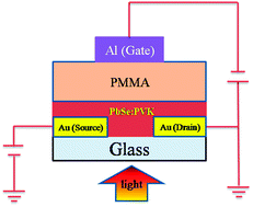
Colloidal quantum dots (CQDs) are promising materials for flexible electronics, light sensing and energy conversion. In particular, as a narrow bandgap semiconductor, lead selenide (PbSe) CQDs have attracted considerable interest due to their potential applications in infrared (IR) optoelectronics such as IR light-emitting diodes (LEDs), photodetectors and solar cells. Solution-processed photodetectors are more attractive owing to their flexible, large-scale and low-cost fabrication, and their performance depends greatly on the film quality and surface morphology. In this study, a high performance solution-processed infrared photodetector based on PbSe CQDs blended with low hole mobility polymer poly(N-vinylcarbazole) (PVK) is presented. In order to obtain a higher device performance, different volume ratios (K = VPVK/VPbSe) of PVK (20 mg ml−1 in chloroform) in PbSe CQDs (15 mg ml−1 in chlorobenzene) were investigated, and a maximum responsivity and specific detectivity of 2.93 A W−1 and 1.24 × 10¹² jones, respectively, were obtained at VG = −20 V under 30 mW cm−2 980 nm laser illumination for field-effect transistor (FET)-based photodetector Au(S&D)/PbSe:
PVK/PMMA/Al(G), in which PbSe
:
PVK nanocomposite with K = 1
:
2 acts as the active layer and poly (methyl methacrylate) (PMMA) as the dielectric layer. The reasons for the high device performance of PbSe
:
PVK nanocomposite as an active layer are discussed, in which PbSe nanoparticles were blended with low hole mobility polymer PVK but showed comparable detectivity as that blended with regioregular P3HT. Moreover, all these types of photodetectors are very stable for reverse fabrication using PMMA dielectric layer to shield the active layer from the environment and by inorganic ligand exchange treatment on the active layer.
As a narrow bandgap semiconductor, lead selenide (PbSe) CQDs are a low-cost solution process, possessing a tunable energy bandgap and high luminescence quantum efficiency.11–13 Various types of nanomaterials, including PbSe CQDs and their nanocomposites, have shown responsive spectra ranging from the ultraviolet to near-infrared,6,14–17 The use of solution-processed thin films of colloidal organic/inorganic semiconductor nanoparticles (or CQDs) as photoconductor active layers has been a critical step for researchers to fabricate low-cost photodetectors.18,19 Being an IV–VI semiconductor with a large Bohr diameter of excitons (46 nm), the electronic structure of PbSe CQDs is strongly quantum confined, and the lowest energy transitions in these materials can be tuned into the near and mid-infrared region. On the other hand, organic semiconductors and/or polymers and CQDs and their nanocomposites have attracted considerable research interests over the past two decades for their use in solid-state optoelectronic devices. To avoid the drawback of low mobility of charge carriers and low photoconductivity that appears in pure polymer-based devices, charge carrier generation can be enhanced, which enables the broadening of photoresponse through their size-tunable optoelectronic properties by blending organic polymers into inorganic CQDs as the active layer. In this way, such a type of optoelectronic devices take advantage of the dependence of the bandgap of CQDs on particle size to absorb (or emit) light in tunable wavelengths.
Among semiconducting polymers, favorable properties of poly(N-vinylcarbazole) (PVK), such as high transparency, good film-forming, mechanical flexibility and its solution process, have attracted significant attention for applications in hybrid organic/inorganic devices.20 PVK is a hole-transporting organic semiconductor (hole mobility μh is much greater than electron mobility μe), which is widely used in organic LEDs (OLEDs), xerography and commonly used as an electro-optically energetic polymer due to its specific photo-physical properties.8 Poly(3-hexylthiophene) (P3HT) is another p-type organic polymer, and a hole mobility of about 0.1 cm2 V−1 s−1 (highest) has been reported21,22 and good device performance has been obtained in photodetectors.23 Therefore, it is reasonable for us to think about what the case would be if we were to use lower hole mobility (between 10−7 and 10−6 cm2 V−1 s−1)24–26 PVK to replace P3HT and to make FET-based IR photodetectors?
Therefore, based on our previous work,23 in this study, first we synthesize size-tailored PbSe CQDs and then incorporate them into the hole-transporting polymer PVK as the active layer to make a field-effect transistor (FET)-based infrared photodetector Au(S&D)/PbSe:
PVK/PMMA/Al(G). Our experimental results showed that the photosensitive spectrum of the PbSe
:
PVK nanocomposite extended into the IR region, and different volume ratios (K = VPVK/VPbSe) of PVK (20 mg ml−1 in chloroform) to PbSe CQDs (15 mg ml−1 in chlorobenzene) were investigated, and a maximum responsivity and high specific detectivity of 2.93 A W−1 and 1.24 × 10¹² jones, respectively, were obtained at VG = −20 V under 30 mW cm−2 980 nm laser illumination for PbSe
:
PVK nanocomposite with K = 1
:
2 as active layer. Our experimental data show that the large interfaces in the PbSe
:
PVK nanocomposites extend an incredible opportunity for efficient exciton dissociation after photogeneration in the PbSe QDs. Efficient exciton dissociation and charge transfer depend on the difference between the potential energy and the electron affinity of the photoactive species. Carrier transport in the nanocomposite layer can be improved under an electric field by the hopping of holes and electrons among the carbazole groups of PVK polymer chains.27 Therefore, in this way, charge transportation in active layer can be enhanced.
First, PVK (Sigma-Aldrich, Mw is 1100
000, purity is 97%) and PbSe CQDs were dissolved in chloroform and chlorobenzene with a concentration of 20 mg ml−1 and 15 mg ml−1, respectively, and then both solutions were blended together at different volume ratios (K = VPVK
:
VPbSe) of K = 2
:
1, 1
:
1 and 1
:
2 by continuous stirring at room temperature for 24 hours to produce the PbSe
:
PVK nanocomposites with uniform and continuous interfaces between PVK and PbSe CQDs.
The concept of a phototransistor, i.e. a photo-field-effect transistor,30 offers an attractive possibility: the gain, united with a lowered dark current as compared to the photoconductor, can be achieved if the thickness of the current-carrying channel can be chosen independently of the thickness of the light-absorbing layer. In the case of conventional FET-based photodetectors, the applied gate bias can modulate the lateral field across the active layer between source and drain electrodes; the electric field causes separation of the photogenerated carriers and greatly extends carrier recombination lifetime, leading to a much higher efficiency. Therefore, herein, we chose the FET configuration to fabricate the photodetectors; its cross-section diagram is shown in Fig. 1. First, an array of 60 nm thick Au electrodes (separated from each other by 100 μm) was deposited on a glass substrate as the source and drain electrodes by thermally evaporating through a shadow mask, which is further contacted with ITO for ease of electrical biasing. Then, the active layer of PbSe:
PVK nanocomposite and dielectric layer of poly(methyl methacrylate) (PMMA) were prepared by spin-coating PbSe
:
PVK nanocomposite and PMMA (80 mg ml−1 in acetone solution) at 2000 rpm and baked at 100 °C and 120 °C, respectively, for 20 min each, forming ∼100 nm active layer and ∼930 nm dielectric layer. Finally, 100 nm Al was thermally evaporated as the gate electrode and annealed at 80 °C for 10 min.
![]() | ||
Fig. 1 Cross-section diagram of the FET-based photodetector and the electrical circuits for its characterization. |
All fabrications were carried out in a nitrogen-filled glove box, and all characterizations were carried out in air at room temperature.
![]() | ||
Fig. 2 TEM image of PbSe CQDs (a) and PVK![]() ![]() ![]() ![]() ![]() ![]() ![]() ![]() ![]() ![]() ![]() ![]() |
In order to confirm the nature of PbSe:
PVK nanocomposite, energy dispersive X-ray (EDX) spectroscopy of PbSe CQDs and PbSe
:
PVK (K = 1
:
2) nanocomposite films on Si substrate, respectively, was carried out. Their intensity peaks are shown in Fig. 3a and b, verifying the presence of all the elements in PbSe
:
PVK nanocomposite. PbSe CQDs and PbSe
:
PVK nanocomposites (K = 1
:
2) were redispersed in tetrachloroethylene and chloroform, respectively, and their absorption spectra are shown in Fig. 4, along with the absorption spectrum of PVK. From here, we can see that the absorption spectrum of PVK peaks at ∼400 nm and there is no absorption in near-infrared region, whereas the absorption spectrum of PbSe peaks at 1200 nm. Obviously, the absorption spectrum of the PVK
:
PbSe nanocomposite is the superposition of the two original constituents, indicating it is only a physical blending process and the presence of PbSe QDs can extend the absorption into the infrared region.
![]() | ||
Fig. 4 Absorption spectra of PbSe![]() ![]() ![]() ![]() |
An appropriate combination of the constituents in the blended nanocomposite contributes to the transport of charge carriers. Therefore, it is easy for one to know that PbSe CQDs play an essential role in terms of the effective absorption of photons in the infrared region. Fig. 5 illustrates the Raman spectrum of the synthesized CQDs, and all the Raman peaks exactly match with the previously reported Raman peaks of PbSe nanocrystals,31,32 confirming the purity of PbSe CQDs. The inset of Fig. 5 demonstrates the X-ray diffraction (XRD) pattern of PbSe CQDs and the PbSe:
PVK nanocomposite. PVK is an organic polymer having no sharp peaks, so the XRD pattern of PbSe
:
PVK nanocomposite will alter with that of PbSe. The XRD pattern of the PbSe CQDs agrees perfectly with PbSe bulk,33,34 and its TEM is also consistent with its XRD pattern. Therefore, one can see that the PVK and PbSe are completely blended with each other. Furthermore, Fourier transform infrared (FTIR) spectra of PbSe nanocrystals, pure PVK and PbSe
:
PVK nanocomposite are shown in Fig. 6. Therefore, all these results could confirm that the synthesized nanocrystals are really PbSe CQDs and the composite formed is really PbSe
:
PVK nanocomposite.
![]() | ||
Fig. 5 Raman spectrum of PbSe nanocrystals; inset shows X-ray diffraction patterns for PbSe nanocrystals (blue) and PbSe![]() ![]() |
![]() | ||
Fig. 6 Fourier transform infrared (FTIR) spectra of PbSe CQDs (black), PbSe![]() ![]() |
In order to improve the performance of the photodetector, we fabricated a field-effect transistor (FET)-based photodetector Au(source & drain)/PbSe:
PVK/PMMA/Al(gate) (see Fig. 1). The main limiting factor for the performance of CQDs-based photodetectors is the high dark current noise due to the narrow bandgap and the high density of the states of PbSe CQDs as the active layer. A disadvantage of PbSe CQDs is their poor stability in ambient air and that they can be destabilized easily; therefore, their applications are limited.35 In order to increase the interparticle coupling and carrier mobility, longer insulating oleate ligands should be exchanged by shorter and more conductive surfactant molecules such as ethanedithiol (EDT) and/or 3-mercaptopropionic acid (MPA).36,37 In our experiments, we performed inorganic ligand exchange on the active layer to enhance the stability of the PbSe CQDs.29 Therefore, unlike the conventional schematic of FET-based device fabrication, a reverse fabricated device was made in our experiments, i.e. the active layer first and then the dielectric layer.23 In this way, the dielectric layer can cover the active layer and prevent it from atmospheric air, and the active layer can be protected from oxidation. Consequentially, an enhanced stability of device can be achieved.23,29 The threshold voltage (Vth) of the FET-based photodetector was measured at VDS = 5 V, and Vth = 3.5 V was obtained, as shown in Fig. 7; other transfer curves at different VDS in dark are shown in the inset (Fig. 7).
![]() | ||
Fig. 7 VG vs. ID (black) at VDS = 5 V, and VG vs. SQRT of ID (blue); the straight line indicates threshold voltage (red); inset shows other transfer curves at different VDS. |
The first feature of a photodetector is sensitivity, the capability of a photodetector to distinguish an incident optical signal from noise.38,39 Photosensitivity (P) of a device can be measured as P = Iphoto/Idark, where Iphoto = Iill. − Idark, and Iphoto is the photocurrent, Iill. shows the drain current under illumination power intensity, and Idark is the drain current in the dark. By using the abovementioned formula for photosensitivity, the photosensitivity of the FET-based photodetector is measured as P = 67.5. The output characteristics of FET-based photodetector Au/PbSe:
PVK/PMMA/Al in the dark and under different illumination intensities are shown in Fig. 8; the curve of photocurrent vs. illumination intensity is shown in the inset. From here, one can see that the photocurrent increases with increasing the illumination intensity up to a certain value, and then the photocurrent is saturated with further increasing of illumination intensity. In our experiments, therefore, we chose 980 nm laser illumination with an intensity of 30 mW cm−2 to illuminate the photodetector.
Photoresponsivity (R) is key factor for characterizing the performance of the photodetectors,27,40 and it is defined by R = Iph/Pill., where Iph = Iill. − Idark, and Pill. is the incident illumination power intensity. The performance of the FET-based photodetectors in which PbSe:
PVK nanocomposite is composed of different K as active layer is listed in Table 1. From here, one can see that the device performance may be enhanced when we increase the volume ratio K to 1
:
2, and a high responsivity of 2.93 A W−1 was obtained for this case. Another important factor for evaluating the performance of a photodetector is its specific detectivity (D*), and it can be defined by the following equation:
![]() | (1) |
Volume ratio of PVK to PbSe | Responsivity (R, A W−1) | Specific detectivity (D*, jones) |
---|---|---|
K = 2![]() ![]() |
0.0266 | 1.13 × 10¹⁰ |
K = 1![]() ![]() |
0.0586 | 2.48 × 10¹⁰ |
K = 1![]() ![]() |
2.93 | 1.24 × 10¹² |
Furthermore, it is natural for someone to ask how can we obtain such a high specific detectivity of a FET-based photodetector with low hole mobility PVK as dopant? To know the reason, we have to know the factors which determine the detectivity of the photodetector. As we know, the performance of the photodetector really depends on the charge carrier mobility, as well as the charge carrier injection barriers at the PVK/QDs' interface. Morphologically, PVK is an amorphous hole-conducting polymer, constituted of linear chains of repeated molecular groups (H2C–HC)n, with suspended carbazole side groups [(C6H4)2NH] randomly arranged around the same chain. Fig. 9 shows the schematic energy-level diagram of materials used in our experiments and the possible charge carrier transport under IR light illumination. The work function (Φ) of Au is about −5.1 eV. The highest occupied molecular orbital (HOMO) energy level and the lowest unoccupied molecular orbital (LUMO) energy level for PVK and PbSe QDs are −5.5 eV and −2.3 eV,41 −5.4 eV and −4.4 eV, respectively. It is worth mentioning that HOMO and LUMO of PbSe CQDs were determined by cyclic voltammetry (not shown here), and they are in agreement with the absorption spectra of PbSe nanocrystals (see Fig. 4) and the energy levels of PbSe QDs reported previously.42 Therefore, the injection barrier for electrons and holes photogenerated in PbSe QDs is about 2.1 eV and 0.1 eV. On the other hand, in the case of being with P3HT, the injection barrier for electrons from PbSe to P3HT is about 1.4 eV, and there is no barrier for holes from PbSe to P3HT. In principle, CQDs absorb photons and then photogenerated holes exit after excitons disassociate at the P3HT/QDs interface and then transfer to P3HT under VDS; however, photogenerated electrons will be trapped and accumulated in CQDs with increasing incident laser intensity,43 forming a built-in electric field at the P3HT/QDs interface, and will increase the potential of the channel, which can be regarded as a floating body effect of the transistor.44,45 Sequentially, the built-in electric field at the P3HT/QDs interface induced by the accumulated electrons will retard the charge transfer at the interface and induce a lower photosensitivity at higher incident light intensity. On the other hand, drift mobilities of both charge carriers are strongly electric field- and temperature-dependent. At room temperature and in an electric field of 2 × 10⁵ V cm−1, the effective hole mobility46 is about 7.14 × 10⁻⁶ cm2 V−1 s−1. The electron mobility47 of P3HT is about 10−9 cm2 V−1 s−1. Basically, device performance depends on the sum of the mobility of electrons and holes, and their mobility in turn can be improved under an electric field; however, hole mobility plays the key role since electrons are minorities in a PVK- or P3HT-based photodetector. We found that the effective mobility of major charge carriers (i.e. holes) in P3HT:
PbSe or PVK
:
PbSe as active layer are of the same order, i.e. ∼1.27 × 10⁻⁴ cm2 V−1 s−1 and ∼4.6 × 10⁻⁴ cm2 V−1 s−1 for PbSe
:
PVK nanocomposite film and PbSe
:
P3HT nanocomposite film, respectively. On the other hand, we noted that the photosensitivity of FET-based photodetector Au/PbSe
:
P3HT/PMMA/Al was less than that of photodetector Au/PbSe
:
PVK/PMMA/Al, and one possible reason may be the occurrence of exciton–exciton annihilation within the P3HT layer at higher light intensity, resulting effectively in a decrease in the exciton lifetime.48 Consequently, the specific photodetectivity will also be reduced, therefore, we got similar specific detectivities in the order of 1012 jones. Certainly, a more detailed theoretical simulation will be carried out for the nonlinear photosensitivity of the device and for the exciton–exciton annihilation within the PbSe
:
P3HT nanocomposite film.
![]() | ||
Fig. 9 Schematic energy-level diagram of each material used in our experiments (a) and charge carriers transport under IR light illumination (b). |
Furthermore, higher D* could be obtained under even weaker incident illumination intensity since D* decreases with increasing incident illumination intensity. Moreover, higher D* could be obtained after further optimizing the device configuration. In this way, by taking advantage of their conductive properties and the size tunability of PbSe QDs, more applications for PbSe nanocrystals and their nanocomposites can be realized in novel optoelectronic devices such as high-sensitivity near/mid infrared photodetectors and high-efficiency solar cells.
This journal is © The Royal Society of Chemistry 2016 |