Bipin Kumar Gupta*a,
Garima Kedawatb,
Pawan Kumarac,
Satbir Singhac,
Sachin R. Suryawanshid,
Neetu Agrawal (Garg)b,
Govind Guptaa,
Ah Ra Kime,
R. K. Guptaf,
Mahendra A. Mored,
Dattatray J. Late*g and
Myung Gwan Hahm*e
aCSIR – National Physical Laboratory, Dr K S Krishnan Road, New Delhi, 110012, India. E-mail: bipinbhu@yahoo.com; Fax: +91-11-45609310; Tel: +91-11-45608284
bDepartment of Physics, Kalindi College, University of Delhi, New Delhi, 110008, India
cAcademy of Scientific and Innovative Research (AcSIR), CSIR – National Physical Laboratory Campus, New Delhi–110012, India
dCentre for Advanced Studies in Materials Science and Condensed Matter Physics, Department of Physics, University of Pune, Pune 411007, India
eDepartment of Advanced Functional Thin Films, Surface Technology Division, Korea Institute of Material Science (KIMS), 797 Changwondaero, Sungsan-GU, Changwon, Gyeongnam 642-831, Republic of Korea. E-mail: mghahm@kims.re.kr
fDepartment of Chemistry, Pittsburg State University, Pittsburg, KS 66762, USA
gPhysical & Materials Chemistry Division, CSIR-National Chemical Laboratory, Pashan Road, Pune 411008, India. E-mail: dj.late@ncl.res.in
First published on 18th January 2016
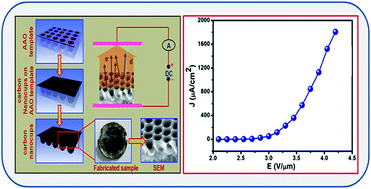
Herein, we design and develop a field emission device utilizing highly porous carbon nanocup (CNC) films. These three-dimensional (3D) low-aspect ratio CNC structures were fabricated by a combination of anodization and chemical vapor deposition techniques. The low turn-on fields of 2.30 V μm−1 were observed to draw an emission current density of 1 μA cm−2 and a maximum emission current density of ∼1.802 mA cm−2 drawn at an applied field of ∼4.20 V μm−1. The enhanced field emission behavior observed from the CNC films is attributed to an excellent field enhancement factor of 1645. The observed field emission properties of CNC arrays are attributed to a synergistic combination of high aspect ratio, nano-sized radius of curvature, highly organized distribution of the emitters over the whole area of specimen and lower screening effect of the CNC arrays. These observations shed light on the effect of the stacking carbon layers of CNC on their electronic properties and open up possibilities to integrate new morphologies of graphitic carbon in nanotechnology applications. Thus, the low turn on field, high emission current density and better emission current stability enable CNC based future field emission applications.
Especially, CNC arrays exhibit several favorable characteristics as an electron source, such as small radius of curvature, outstanding chemical inertness, exceptional thermal stability, and high mechanical strength. CNC films incorporated with millions of truncated conical graphitic structures, different from conventional CNTs made up of multi-seamless cylinders of hexagonal carbon networks.6,15 The cup-like nano-structure provides a hollow tubular morphology. It differs from other quasi-one dimensional (1D) carbon structures, which normally behave as quasi-metallic conductors of electrons. Some of 1D carbon structures exhibit semiconducting behaviors due to their chirality.16 Such structure provides a large portion of exposed and reactive edges with abundant dangling bonds both on the outer surface and in the inner channel. Additionally, the chemical activity of the inner channel is even higher due to highly strained curvature.17 Therefore, the utilization of these exposed edges of CNCs to chemical functionalization or surface modification opens up new avenues in absorbent materials, composites, field emitters and gas storage components. For the practical application to field emission sources, the growth of periodic array of CNCs on a large area with high packing density is necessary. CNC has low-aspect ratio (1:
1.2) showing good emission performance with flat thin film nature which is highly required in FED based display panels; it has been shown in our experiment, which has not been reported earlier. In recent years, anodic aluminum oxide (AAO) nano-templates based approaches have been widely introduced to fabricate well-aligned periodic arrays of nanostructure.
Herein, we proposed and demonstrated a high performance field emission device with vertically aligned 3D and low aspect-ratio CNCs structure. The highly organized CNC arrays were grown by chemical vapor deposition (CVD) using a short channel AAO template. Fig. 1 shows a schematic diagram of the fabrication approach for CNC films with their counterparts of scanning electron microscope (SEM) image and appearances of the as-grown sample. The simple field emission device utilizing CNC films was fabricated as shown in schematic drawing (Fig. 1). The field emission measurements showed that carbon nanocup arrays-based field emission device had outstanding performance although these have low-aspect ratio. It is suggested that the open edges on the CNCs act as active emission sites in vertically aligned 3D CNC structure giving enhanced emission characteristics.
Under the above-explained experimental conditions of synthesis using CVD method, the formation of carbon nanocups can be explained by the controlled growth of graphene films in the predesigned AAO nanochannel template. At the temperature of around 660 °C, carbon atoms begin to be adsorbed on the substrate and the graphene islands begin to nucleate. This leads to the formation of flat epitaxial graphene sheet on the AAO template. Since the graphene growth consumes carbon atoms, thus the carbon source supply is done for a judiciously calculated period of time. As soon as, the carbon concentration is below super saturation, the nucleation and growth of graphene islands would be finished.
The D band at 1350 cm−1 (the disorder-induced band), and G band at 1600 cm−1 (the tangential modes of graphitic structures) are typically presented in graphitic structures and their AD/AG ratio is 0.81, indicating the high degree of disorder on the as-synthesized CNC structure due to catalyst-free CVD process. Also, the G band respresents the in-plane stretching vibrations of the sp2-carbon–carbon bonds within the ordered graphitic layers of CNCs.16,19,20 The synthesized cup-like carbon nano-structures are comprised of multi-layered graphitic layers. X-ray photoelectron spectroscopy (XPS) clearly revealed the presence of carbon, oxygen, and aluminum elements of CNC films as shown in Fig. 2d. To determine the chemical component and the oxidation state of carbon element, high-resolution XPS spectra of C 1s are curve-fitted into three contribution peaks appearing at 284.2, 286.0 and 288.0 eV (Fig. 2e). The main peak at 284.2 eV is assigned to sp2-hybridized graphite-like carbon atoms (C–C bond). The peaks at 286.0 and 288.0 eV are typical of carbon atom bound to one oxygen atom by double bond (CO bond) and to two oxygen atoms (O–C
O bond), respectively.21 It signifies that the oxygen-containing functional groups are sequentially introduced onto the surfaces of the tubes. The core level peak of the Al (2p) region for CNCs is also shown at 78.6 eV binding energy in Fig. 2f. The presence of Al element is due to the AAO templates.
The scanning electron microscope (SEM) and transmission electron microscope (TEM) micrographs of a highly organized CNC structures after removing the AAO template are shown in Fig. 3. The SEM images of top view of CNC arrays (Fig. 3a) and side view of CNC arrays (Fig. 3b) clearly show their low-aspect ratio structures with a cup diameter of ∼100 ± 2 nm and length of ∼120 ± 2 nm. The CNC arrays have a well-organized, interconnected structure and a highly porous surface morphology with very sharp edges (thickness ∼ 5–10 nm) on a diameter. This highly porous, low-aspect ratio nanocup structure provides a large specific surface area, which indicates that the walls of vertically aligned CNTs give exuberance of surface in nanocups.6,20 The additional surface area on the CNC nano-structure enhances the electrochemical properties and optical properties of devices by providing a large area for the electrolyte ions to interact with the electrode surface.
The top view morphology for another CNCs sample has also investigated (Fig. S1; see ESI†). The TEM image of connected array of CNCs (Fig. 3c) has a large hollow core along their length with ∼100 nm inner diameter and ∼120 nm length demonstrates the formation of wide scale CNCs. The high-resolution TEM (HRTEM) image is shown in Fig. 3d and inset shows its magnified view; which has been taken from the blue square region. It reveals the graphitic layers of CNCs corresponding to (002) plane with an interplanar spacing of 0.34 nm. Since CNCs exhibit enormously active diameter with sharp edges.
The template-assisted synthesis of the CNCs can be controllably grown by the chemical vapour deposition. The CNC films have numerous sharp edges and enormous proportion of nano-protrusions. Due to the unique morphology of the nanocups, field emission performance should be enhanced. The field emission measurement instrument is shown in Fig. S2 (see ESI†). In the electron field emission experiments, the cathode was the supported CNTs film and the anode was a probe (0.63 mm in diameter) positioned at a distance d ∼ 1 mm above the surface. The cathode connection was via the CNC film. The samples were mounted on a ceramic holder in a high vacuum chamber. After the chamber reached a base pressure below 5 × 10⁻⁵ Pa and the field emission was initiated by cycling the voltage applied to the probe up to 1000 V for five times. After a pause of about 0.5 h at zero electric field, the field emission current was recorded as a function of voltage (V) applied to the probe. The Fowler–Nordheim (F–N) equation for field emitters deposited on flat substrates in the form of thin film, has been modified to yield an equation in terms of current density (J) and the applied electric field (E = V/d, where V is the voltage applied between the flat cathode and the anode screen, and d is their separation). The modified F–N equation is as follows,22–25
J = λMa(β2E2/Φ)exp(−bΦ3/2νF/βE) | (1) |
Furthermore, the field emission behaviour of CNC sample from 1st to 6th cycle runs are shown in the Fig. S3a (see ESI†). All tested samples show better emission uniformity and a good reproducibility of field emission behaviour during the initial 6 cycle run. In addition to the cyclability test, the field emission characteristics of different as-synthesized CNC samples (sample 1, sample 2, sample 3, sample 4 and sample 5) are also examined to explore reproducibility and the results are shown in Fig. S3b (see ESI†). It can be noticed that all the samples are showing almost similar and consistent behaviour.
In the case of CNC films, emission occurs from multiple emitters and an integrated current is measured. There could be lots of variations in local fields due to various geometries of the emitters. Also, the exact analysis of field emission characteristics of CNC arrays is difficult owing to work function of each emitter is not necessarily same. However, it may be noted that CNCs provide a hollow tubular morphology unlike that of conventional CNTs, which are made up of seamless cylinders of hexagonal carbon network. Compared to nanotubes, the nanocups have a greater amount of exposed inner surfaces and edges for modification sites. Thus, the observed superior values of turn-on and threshold field, and extraction of high emission current density at lower applied electric field is attributed to the synergic effect of: (a) an optimum length and density combination to overcome screening effect, (b) sharp closed tips and (c) open edges on the outer surface of CNTs which enhance the local field.26–28 These open edges also act as additional emission sites.29 Moreover, other favorable conditions for enhanced emission of such periodic structured conical CNTs could be: (a) hydrogen saturation of open edges on the surface which also decrease the effective work function, (b) nano-sized radius of curvature and (c) highly ordered distribution of the emitters over the whole area of specimen. The cup morphology increases the specific surface area of the sample which reduces the effective density and hence an extremely reduced electric field screening.30,31 Furthermore, the formation of sharp bends at the bottom caps where carbon atoms show sp3 like atomic bonds instead of sp2 configuration.32 This change in coordination would decrease the height of potential barrier and hence could explain the very low work function as can estimated from the Fowler–Nordheim plots. As predicted, the H- or O-terminated edges greatly effects the net work function. Simulation studies predict the work function of 6.3 eV for a clean edge graphene as compared to the work functions of 3.31 and 7.29 eV respectively for H- and O-terminated edge.33 Thus, the observed superior values of turn-on and threshold field, and extraction of high emission current density at lower applied electric field is attributed synergic effect of low aspect ratio, sharp diameter of the cups, uniform distribution of the emitters over the whole area of specimen and lower screening effect of the CNCs.30,31 However, the performance of CNCs is lower as compared to other carbon based materials, because CNCs nanostructure associated with large number of nano-cup structures in form of array, where each cup have non-uniform dimensions from top to bottom like other carbon materials i.e. CNT. Therefore, the electric field at the base of individual CNCs structures increases the number of emitter points; as a result the overall electric field strength reduces at the base because of enhanced screening effect.30,31
The F–N plot by a plotting the graph of ln(J/E2) versus 1/E for the CNCs is shown in Fig. 4b with a calculated field enhancement factor of ∼1645 from slope of the linear region of F–N plot. The F–N plot for the CNCs field emitter is nearly linear and shows a tendency for saturation at high electric fields. The field enhancement factor can give idea of the enhancement of the electric field at the emitter sites due to sharp edges with their huge nanometric protrusions. In the present case, the field enhancement factor is calculated from the slope of the F–N plot and is found to be ∼1645 by assuming work function (ϕ) of the emitter ∼5 eV for CNCs. Fig. 4c shows the typical long-term current stability (I–t) from a CNCs field emitter recorded at a base pressure of ∼1 × 10⁻⁸ mbar. To increased performance of CNCs in device applications point of view, cathode requires nearly constant emission current stability, so it is a decisive and important parameter in the fabrication of field emission based nanoelectronic devices. Fig. 4c show the field emission current stability traces for CNCs at ∼8 μA preset value of current for a sampling interval of 10 seconds recorded over a period of 8 hours. The average emission current is seen to be stable over the duration of the measurement characterized by fluctuations in the form of “spikes”. The appearance of the “spikes” in the emission current is attributed to the field induced adsorption, desorption, and migration of the residual gas molecules on the emitter surface. The striking feature of the field emission behaviour of the CNCs emitter is that the average emission current remains constant over the entire duration and shows no signs of the detrimental effects, signalling its mechanical robustness against ion bombardment and field-induced stress. Fig. 4d shows the typical field emission micrograph of the CNCs field emitter recorded at a current density of ∼500 μA cm−2 consists of a large number of tiny bright spots indeed emission is from most of the protruding CNCs field emitter. The emission picture of CNC was taken from certain height from top window FED instrument. Therefore, exact distribution of emission intensity cannot be visible as uniform as it is. Thus, this new architecture of CNC encourages for further research to be done establishing CNC as a promising next-generation efficient material for FED devices.
Footnote |
† Electronic supplementary information (ESI) available. See DOI: 10.1039/c5ra25682h |
This journal is © The Royal Society of Chemistry 2016 |