
Fabrication of ordered Si nanopillar arrays for ultralow reflectivity
Fei Teng,
Ning Li,
Lingxiao Liu,
Daren Xu,
Dongyang Xiao and
Nan Lu*
State Key Laboratory of Supramolecular Structure and Materials, College of Chemistry, Jilin University, Changchun 130012, PR China. E-mail: luenan@jlu.edu.cn; Fax: +86-431-85168477; Tel: +86-431-85168477
First published on 1st February 2016
Abstract
The reduction of surface reflectivity is an important approach to improve the performance of optical and optoelectronic devices. Herein, we greatly suppressed the reflectivity of the silicon surface by ordered silicon nanopillar arrays, which were fabricated by metal-assisted chemical etching. The average reflectivity of the silicon surface was suppressed to lower than 0.1% from 45% at the wavelength range of 250–1050 nm, and it remained below 1.2% when the incident angle changed from 0° to 70°. We investigated the effect of the height and diameter of the nanopillars on the reflectivity, which revealed that the reflectivity decreased with increasing height of the nanopillars, and the reflectivity peaks blue shifted with the reducing nanopillar diameter. The results indicate that the antireflection performance can be tuned by adjusting the height and diameter of nanopillars. Therefore, this method may provide an approach to reduce and tune the reflection of Si surfaces.
Introduction
Surface reflection results from the change of the reflective index when light passes through the interface of two kinds of materials. In visible wavelengths, the reflectivity of the silicon surface is up to 40% due to its high reflective index. This phenomenon seriously limits the performance of the optical and photoelectrical devices based on silicon, such as solar cells, photodetectors and displays.1–3 The observation of moth eyes inspired scientists to suppress the reflectivity by introducing subwavelength structures on the surfaces.4–6 Various nanostructures have been fabricated to reduce the reflectivity of silicon surface, such as nanocones, nanopillars, nanoporous, nanowires, and pyramidal structures.7–11 When the dimension of the structure formed on the substrate is in the same scale with the wavelength of the incident light, the incident light can be redirected inside the gradient refractive index layer. This multiple reflection and scattering process can greatly increase the optical length of the incident light, and cause more incident light to be absorbed.12 The increase of the aspect ratio of the nanostructures increases the chance for light being reflected and scattered in the nanostructures, which brings more opportunities for light being absorbed and lower surface reflectivity. Therefore, more efforts have been devoted to enhance aspect ratio of the nanostructures to decrease reflectivity. Some methods have been proposed to fabricate nanostructures with high aspect ratio on silicon based on dry etching and wet etching. Huang et al.13 fabricated aperiodic silicon nanotip structures with aspect ratio of 80![[thin space (1/6-em)]](https://www.rsc.org/images/entities/char_2009.gif) :1 by a high-density electron cyclotron resonance plasma etching, reducing the average reflectivity to lower than 1% at the wavelength from 500 to 2500 nm. Smyrnakis et al.14 created order silicon nanowire (SiNW) arrays with aspect ratio of 37:1, using e-beam lithography and cryogenic Si plasma etching, the reflectivity was decreased to 2% in the range of 250–950 nm. We fabricated biomimetic corrugated silicon nanocone arrays to increase the aspect ratio based on twice reactive ion etching (RIE) with polystyrene spheres as masks. The reflectivity was reduced to 0.7% in the range of 400–1050 nm.15 To increase the aspect ratio of structure, we tried to fabricate another hierarchical array based on the combination of nanoimprint lithography and self-assembly, which suppressed the reflectivity to lower than 5% in the range of 300–1100 nm.5 All the above structures were fabricated with dry etching. Compared to dry etching method, metal-assisted chemical etching is an easy method for fabricating nanostructures of high aspect ratio.16–18 Kumar et al. fabricated SiNW arrays for silicon based solar cells through metal-assisted chemical etching, the SiNW arrays performed low reflectivity (<5%) over 400–1100 nm spectral range.19 Moreover, a few works reported that SiNWs were fabricated by galvanic wet etching and exhibited spectral reflectivity less than 0.1% in the range of 200–850 nm.20,21 We enhanced the aspect ratio of nanostructures in the hierarchical structures with metal-assistant chemical etching previously.22 However, the arrangement and size of the SiNWs cannot be controlled by these methods, so it is difficult to regulate the antireflection properties, which will limit the applications of silicon materials.
:1 by a high-density electron cyclotron resonance plasma etching, reducing the average reflectivity to lower than 1% at the wavelength from 500 to 2500 nm. Smyrnakis et al.14 created order silicon nanowire (SiNW) arrays with aspect ratio of 37:1, using e-beam lithography and cryogenic Si plasma etching, the reflectivity was decreased to 2% in the range of 250–950 nm. We fabricated biomimetic corrugated silicon nanocone arrays to increase the aspect ratio based on twice reactive ion etching (RIE) with polystyrene spheres as masks. The reflectivity was reduced to 0.7% in the range of 400–1050 nm.15 To increase the aspect ratio of structure, we tried to fabricate another hierarchical array based on the combination of nanoimprint lithography and self-assembly, which suppressed the reflectivity to lower than 5% in the range of 300–1100 nm.5 All the above structures were fabricated with dry etching. Compared to dry etching method, metal-assisted chemical etching is an easy method for fabricating nanostructures of high aspect ratio.16–18 Kumar et al. fabricated SiNW arrays for silicon based solar cells through metal-assisted chemical etching, the SiNW arrays performed low reflectivity (<5%) over 400–1100 nm spectral range.19 Moreover, a few works reported that SiNWs were fabricated by galvanic wet etching and exhibited spectral reflectivity less than 0.1% in the range of 200–850 nm.20,21 We enhanced the aspect ratio of nanostructures in the hierarchical structures with metal-assistant chemical etching previously.22 However, the arrangement and size of the SiNWs cannot be controlled by these methods, so it is difficult to regulate the antireflection properties, which will limit the applications of silicon materials.
In this work, we fabricated ordered silicon nanopillar (SiNP) arrays based on metal-assisted chemical etching. The height of the SiNP arrays was tuned by adjusting the etching duration. With the optimized SiNP arrays, the average reflectivity of silicon surface was suppressed to lower than 0.1% from 250 to 1050 nm, and it remained below 1.2% with the incident angle ranging from 0° to 70°. In addition, we investigated the correlation of the characteristic parameters of SiNP arrays and the antireflective properties, the results indicate that the antireflection performance can be tuned by adjusting the characteristic parameters of SiNP arrays. Compared with our previous work for generating SiNP arrays based on RIE,23,24 this chemical method is simpler, less expensive, and easier to get high aspect ratio SiNPs, which allows for the ultralow reflectivity.
Experimental section
Materials
Acetone, chloroform, ethanol, toluene and nitric acid (HNO3) were analytic grade reagents and purchased from commercial sources. The monodisperse polystyrene (PS) spheres, Ag and Au sheets (99.999%), potassium iodide (KI) and iodine (I2) were purchased from Sigma Aldrich Co. Si wafers [n type (100)] were obtained from Youyan Guigu (Beijing, China).Fabrication of the metal nanohole template
Silicon substrate was cut into 1.5 cm × 1.5 cm slides, and then they were subsequently sonicated in acetone, chloroform, ethanol, and deionized water for 5 min respectively to remove organic contaminants. Then the Si slides were immersed in a mass fraction of 4% aqueous solution of hydrogen fluoride for 2 min to remove passivation layer of silicon surface and dried with nitrogen. The monolayer of 630 nm PS spheres was prepared according to ref. 25. Briefly, the monolayer of PS spheres was prepared by spreading 0.2 mL 5% (mass ratio) monodispersed PS spheres on the surface of water in a glass tank, and then the assembled monolayer of PS spheres was transferred onto Si slides, and then dried under room temperature. Then the monolayer of PS spheres on Si slide was subjected to reactive ion etching (RIE) process on a Plasmalab Oxford 80 Plus (ICP65) system with O2 to reduce the diameter of the PS spheres. The diameter of the PS spheres was controlled by tuning the RIE duration. In this work, the diameter of the PS spheres was reduced to 475, 430, 418 and 388 nm by setting the duration at 6, 6.5, 7 and 8 min respectively. In order to obtain fine morphology of created structures, a 7 nm Ag film and 15 nm Au film were successively deposited on the substrate by thermal evaporation as catalyst.26 After lifting off the PS spheres with toluene in ultrasonic bath, the metal template was obtained.Formation of the SiNPs
Metal-assisted chemical etching was carried out to form SiNPs. At room temperature (24–26 °C), a Si slide with the metal template was immersed into the solution of hydrofluoric acid:hydrogen peroxide:deionized water with volume ratio of 20:3: 80, after that, the Au film was removed by KI/I2 mixture solution according to ref. 27, the mixing mass ratio of KI:I2:H2O was 4:1:40. The Ag film was removed by 10% HNO3 solution. Finally, the ordered array of vertically aligned SiNPs was created.
Characterization
Scanning electron microscope (SEM) images were taken on HITACHI SU8020 field emission SEM with primary electron voltage of 3 kV, and reflective spectra were recorded on R1-A-UV series spectroscopy meter (Shanghai Ideaoptics Technology Co., Ltd., China).Results and discussion
Fig. 1 shows the schematic diagram of the process for fabricating SiNP arrays. The fabrication details are described in the Experimental section. | ||
| Fig. 1 Schematic illustration for the fabrication of the SiNP arrays. (a) Reducing the diameter of PS spheres by RIE process. ((b) and (c)) Depositing a 7 nm silver film and 15 nm gold film by thermal evaporation successively. (d) Removing PS spheres with toluene. (e) Creating SiNP arrays by metal-assisted chemical etching. | ||
Fig. 2(a) shows the monolayer of 630 nm PS spheres. After reducing the diameter of PS spheres to 430 nm by RIE, the PS spheres are separated, as revealed in Fig. 2(b). And then the metal hole array is observed by removing residual PS spheres after successively depositing Ag and Au films, as shown in Fig. 2(c), which is used subsequently as template for metal-assisted etching.
 | ||
| Fig. 2 SEM images of (a) and (b) monolayer of PS spheres before and after reduction, and (c) metal hole array. The diameter of PS spheres in (a) and (b) is 630 and 430 nm respectively. The period of the array is 630 nm, and the diameter of the metal holes is 430 nm. | ||
Using the same metal array (shown in Fig. 2(b)) as etching template, SiNPs with different heights were fabricated by tuning the etching durations. As shown in Fig. 3, the height of the SiNPs can be adjusted from 0.92 μm to 12.46 μm by setting the etching duration ranging from 10 to 70 min. The etching durations for Fig. 3(a) to (h) are 10, 15, 20, 30, 40, 50, 60 and 70 min respectively. The average heights of the SiNPs of Fig. 3(a) to (h) were about 0.92, 1.55, 3.40, 5.08, 6.16, 7.48, 9.75 and 12.46 μm respectively. Fig. 3(i) shows that the correlation of the average height of SiNPs and the etching duration is nearly linear, and the fluctuation in etching rate could be caused by the instability of the room temperature. As revealed in the insets, the SiNP arrays are hexagonal arranged when the average height of SiNPs is shorter than 5.08 μm, however, they aggregated at the tops when their average height is 6.16 μm and longer than 6.16 μm and more aggregations are formed when the average height of SiNPs increases. It has been reported that for the high aspect ratio SiNPs, the capillary force is greater than the supportive forces of the SiNPs during the drying process, and the SiNPs bend and aggregate at the top.28
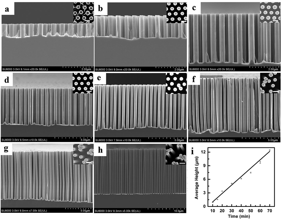 | ||
| Fig. 3 (a–h) SEM images of the SiNPs with different heights. (a) 0.92 μm, (b) 1.55 μm, (c) 3.40 μm, (d) 5.08 μm, (e) 6.16 μm, (f) 7.48 μm, (g) 9.75 μm, (h) 12.46 μm. (i) Correlation of the average heights of SiNPs and the etching duration. Insets in (a–h) show the corresponding top views. Scale bars are 500 nm for the insets. | ||
The comparison of the reflectivity for the SiNPs and silicon wafer is shown in Fig. 4(a). The spectra indicate that the reflectivity of Si wafer can be greatly suppressed by the SiNPs, and it decreases with the increase of the average height of SiNPs. The average reflectivity can be even reduced to lower than 0.1% at the range of 250–1100 nm by the SiNPs of 12.46 μm in average height, with the aspect ratio of 29:1. The height of the SiNPs is the thickness of the gradient refractive index layer, so the increase of the height of SiNPs can decrease the gradient in the change of refractive index. Fig. 4(a) shows that there were wavy peaks at the wavelengths of 700–1050 nm in the reflective spectra when the average height was lower than 5.08 μm. For nanopillars, the period and diameter are in the same scale of wavelength, but the height is longer than wavelength, so the light rays are trapped among nanopillars leading to the multiply effects,29 which include the absorption along with the length of SiNPs, diffraction by the period arrays, coupling effect of incident light between adjacent SiNPs, and resonances caused by the reflection from the top and bottom of SiNPs.30 These effects can be ruled out with large pitch.31 In this work, when the average height increases to 6.16 μm, a broad peak appeared instead of the wavy peaks. This phenomenon may be caused by the aggregation of SiNPs, which break up the period of SiNP array and shorten the distance between adjacent SiNPs, as revealed in the insets in Fig. 3(e) to (h).
 | ||
| Fig. 4 (a) Reflective spectra of the SiNP arrays with different heights. (b) Correlation of the SiNP heights and the average reflectivity at wavelengths of 250–1050 nm. (c) Measured angle-dependent reflective spectra of the SiNP arrays. | ||
The correlation of the SiNP heights and the average reflectivity at the wavelengths of 250–1050 nm is shown in Fig. 4(b), which shows that the average reflectivity decreased with increasing the average height of SiNPs. The reduction rate of average reflectivity is nearly uniform when the average height of SiNPs is lower than 6.16 μm, however, it becomes slower when the average height of SiNPs is higher than 6.16 μm. The increase of optical length and more light absorption leads to the reduction of reflectivity. But the aggregation of the SiNPs on the tops of SiNPs makes the tops of SiNPs like reflective surfaces, and the sidewalls of SiNPs like inclined planes, which decreased the light absorption and optical length, leading to lower reduction rate of reflectivity.
To investigate the effect of the incident angle on the reflectivity, the reflective spectra of the SiNPs at different incident angles for un-polarized light were collected and shown in Fig. 4(c). No obvious change can be observed in the reflective spectra when the incident angle is smaller than 50° in the wavelength region of 250–1050 nm. The reflectivity remains below 0.1% at the wavelengths of 250–670 nm, and it remains below 0.3% from 670 to 1050 nm. When the incident angle is lager than 60°, there is an abrupt variation in the reflectance spectra. The reflectivity is below 1.2% even the incident angle increased to 70°. The SiNP arrays exhibits good antireflection performance in wide angles. The sharp peaks at 655 nm in Fig. 3(a) and (c) are caused by the light source of ultraviolet lamp.
Furthermore, we investigated the effect of the diameters of SiNPs on the antireflection. The PS spheres with 475, 418 and 388 nm in diameter were used to fabricate different sizes of metal hole arrays, as presented in Fig. 5(a) to (c). The roughness of the edge of metal holes increases with the reduction of the PS spheres. This is because longer RIE duration is applied to make PS spheres smaller, while extending the etching process can introduce more roughness to the surface of PS spheres. With these metal hole arrays as etching masks, the SiNPs with different diameters, same height (2 μm) and same period (630 nm) were fabricated, as shown in Fig. 5(d) to (i). The SEM images reveal that the roughness of the SiNPs sidewall increases with the reduction of the diameter of SiNPs.
 | ||
| Fig. 5 (a–c) SEM images of the metal holes with different diameters. (d–i) The top-view and the corresponding side-view SEM images of the SiNPs with different diameters. | ||
It can be observed that there are some wavy reflective peaks in Fig. 6(a). In principle, the spectral location of reflective peaks can be approximated by the equation:32
| λ = neffP | (1) |
 | ||
| Fig. 6 (a) Reflective spectra and (b) average reflectivity of the SiNPs with different diameters. The period and height is 630 nm and 2 μm respectively. | ||
Fig. 6(b) shows the average reflectivity of the SiNPs with different diameters over every 100 nm band. There is little difference when the wavelength is lower than 550 nm. The average reflectivity of SiNPs with 475 nm in diameter is the lowest in the range of 550–650 nm and 850–950 nm. The average reflectivity of SiNPs with diameter of 418 nm is the lowest at 750–850 nm and 950–1050 nm. For the SiNPs with 388 nm in diameter, the average reflectivity is the lowest in the range of 650–750 nm. For SiNPs with the same period and height, the diameter influences the antireflection band. It makes it possible to adjust the antireflection band by controlling the diameter of nanopillars.
Conclusions
We fabricate ordered SiNP arrays with the aspect ratio of 29:1 by metal-assisted chemical etching. With the SiNPs, the average reflectivity of Si is suppressed to lower than 0.1% from 45% at the wavelengths of 250–1050 nm. Furthermore, the reflectivity remains lower than 1.2% when the angle of incident light changes from 0° to 70°. The reflectivity decreases with increasing the height of nanopillars, and the reflective peaks blue shift with decreasing the diameter of SiNPs, which allows for tuning the reflectivity by designing nanostructures. The ordered SiNPs may be applied in solar cells, photoelectrochemical conversions, photodetectors, and biosensors.
Acknowledgements
This work was supported by the National Natural Science Foundation of China (No. 21273092).Notes and references
- J. S. Yoo, I. O. Parm, U. Gangopadhyay, K. Kim, S. K. Dhungel, D. Mangalaraj and J. S. Yi, Sol. Energy Mater. Sol. Cells, 2006, 90, 3085–3093 CrossRef CAS.
- T. Glaser, A. Ihring, W. Morgenroth, N. Seifert, S. Schroter and V. Baier, Microsyst. Technol., 2005, 11, 86–90 CrossRef CAS.
- Y. M. Song, Y. Z. Xie, V. Malyarchuk, J. L. Xiao, I. Jung, K. J. Choi, Z. J. Liu, H. Park, C. F. Lu, R. H. Kim, R. Li, K. B. Crozier, Y. G. Huang and J. A. Rogers, Nature, 2013, 497, 95–99 CrossRef CAS PubMed.
- S. A. Boden and D. M. Bagnall, Appl. Phys. Lett., 2008, 93, 133108–133110 CrossRef.
- H. B. Xu, N. Lu, G. Shi, D. P. Qi, B. J. Yang, H. Li, W. Xu and L. F. Chi, Langmuir, 2011, 27, 4963–4967 CrossRef CAS.
- J. W. Leem, Y. M. Song and J. S. Yu, Nanoscale, 2013, 5, 10455–10460 RSC.
- J. Zhu, Z. Yu, G. F. Burkhard, C. M. Hsu, S. T. Connor, Y. Xu, Q. Wang, M. McGehee, S. Fan and Y. Cui, Nano Lett., 2009, 9, 279–282 CrossRef CAS PubMed.
- B. Kiraly, S. Yang and T. J. Huang, Nanotechnology, 2013, 24, 245704–245713 CrossRef PubMed.
- B. S. Kim, D. H. Lee, S. H. Kim, G. H. An, K. J. Lee, N. V. Myung and Y. H. Choa, J. Am. Ceram. Soc., 2009, 92, 2415–2417 CrossRef CAS.
- S. K. Srivastava, D. Kumar, S. W. Schmitt, K. N. Sood, S. H. Christiansen and P. K. Singh, Nanotechnology, 2014, 25, 175601–175617 CrossRef PubMed.
- S. C. Baker-Finch and K. R. McIntosh, Prog. Photovoltaics, 2011, 19, 406–416 CAS.
- J. Yang, F. Luo, T. S. Kao, X. Li, G. W. Ho, J. Teng, X. Luo and M. Hong, Light: Sci. Appl., 2014, 3, e185–192 CrossRef CAS.
- Y. F. Huang, S. Chattopadhyay, Y. J. Jen, C. Y. Peng, T. A. Liu, Y. K. Hsu, C. L. Pan, H. C. Lo, C. H. Hsu, Y. H. Chang, C. S. Lee, K. H. Chen and L. C. Chen, Nat. Nanotechnol., 2007, 2, 770–774 CrossRef CAS PubMed.
- A. Smyrnakis, E. Almpanis, V. Constantoudis, N. Papanikolaou and E. Gogolides, Nanotechnology, 2015, 26, 085301–085312 CrossRef CAS PubMed.
- Y. D. Wang, N. Lu, H. B. Xu, G. Shi, M. J. Xu, X. Lin, H. Li, W. Wang, D. Qi, Y. Lu and L. Chi, Nano Res., 2010, 3, 520–527 CrossRef CAS.
- A. Najar, J. Charrier, P. Pirasteh and R. Sougrat, Opt. Express, 2012, 20, 16861–16870 CrossRef CAS.
- J. Yeom, D. Ratchford, C. R. Field, T. H. Brintlinger and P. E. Pehrsson, Adv. Funct. Mater., 2014, 24, 106–116 CrossRef CAS.
- F. Bai, M. Li, R. Huang, Y. Li, M. Trevor and K. P. Musselman, RSC Adv., 2014, 4, 1794–1798 RSC.
- D. Kumar, S. K. Srivastava, P. K. Singh, M. Husain and V. Kumar, Sol. Energy Mater. Sol. Cells, 2011, 95, 215–218 CrossRef CAS.
- H. C. Chang, K. Y. Lai, Y. A. Dai, H. H. Wang, C. A. Lin and J. H. He, Energy Environ. Sci., 2011, 4, 2863–2869 CAS.
- Y. A. Dai, H. C. Chang, K. Y. Lai, C. A. Lin, R. J. Chung, G. R. Lin and J. H. He, J. Mater. Chem., 2010, 20, 10924–10930 RSC.
- D. P. Qi, N. Lu, H. B. Xu, B. J. Yang, C. Y. Huang, M. J. Xu, L. G. Gao, Z. X. Wang and L. F. Chi, Langmuir, 2009, 25, 7769–7772 CrossRef CAS PubMed.
- H. B. Xu, N. Lu, D. P. Qi, J. Y. Hao, L. G. Gao, B. Zhang and L. F. Chi, Small, 2008, 4, 1972–1975 CrossRef CAS PubMed.
- H. Xu, N. Lu, D. Qi, L. Gao, J. Hao, Y. Wang and L. Chi, Microelectron. Eng., 2009, 86, 850–852 CrossRef CAS.
- J. Rybczynski, M. Hilgendorff and M. Giersig, NATO Sci. Ser., 2003, 91, 163–172 CAS.
- S. M. Kim and D. Y. Khang, Small, 2014, 10, 3761–3766 CrossRef CAS PubMed.
- The gold etching online, http://www.microchemicals.eu/technical_informationhttp://www.microchemicals.eu/technical_information, accessed December 2009.
- Z. Zuo, K. Zhu, G. Cui, W. Huang, J. Qu, Y. Shi, Y. Liu and G. Ji, Sol. Energy Mater. Sol. Cells, 2014, 125, 248–252 CrossRef CAS.
- J. G. Cai and L. M. Qi, Mater. Horiz., 2015, 2, 37–53 RSC.
- B. C. Sturmberg, K. B. Dossou, L. C. Botten, A. A. Asatryan, C. G. Poulton, C. M. de Sterke and R. C. McPhedran, Opt. Express, 2011, 19(5), A1067–A1081 CrossRef CAS PubMed.
- K. Seo, M. Wober, P. Steinvurzel, E. Schonbrun, Y. Dan, T. Ellenbogen and K. B. Crozier, Nano Lett., 2011, 11, 1851–1856 CrossRef CAS PubMed.
- I. D. Block, N. Ganesh, M. Lu and B. T. Cunningham, IEEE Sens. J., 2008, 8, 274–280 CrossRef CAS.
| This journal is © The Royal Society of Chemistry 2016 |