Electron transport study on functionalized armchair graphene nanoribbons: DFT calculations

E. Gracia-Espinoabc, F. López-Urías*c, H. Terronesd and M. Terronesef
aDepartment of Physics, Umeå University, S-90187 Umeå, Sweden
bDepartment of Chemistry, Umeå University, S-90187 Umeå, Sweden
cAdvanced Materials Department, IPICYT, Camino a la Presa San José 2055, Col. Lomas 4a sección, San Luis Potosí S.L.P. 78216, México. E-mail: flo@ipicyt.edu.mx
dDepartment of Physics, Applied Physics and Astronomy, Rensselaer Polytechnic Institute, Troy 12180, USA
eDepartment of Physics and Center for 2-Dimensional and Layered Materials, The Pennsylvania State University, University Park, PA 16802, USA
fDepartment of Chemistry, Department of Materials Science and Engineering and Materials Research Institute, The Pennsylvania State University, 104 Davey Lab., University Park, PA 16802-6300, USA

Received 28th November 2015 , Accepted 16th February 2016

First published on 17th February 2016


Abstract

Quantum transport studies are performed on doped and functionalized 8- and 11-armchair graphene nanoribbons (aGNRs) by means of density functional theory. Substitutional doping is performed by introducing boron, nitrogen, oxygen, silicon, phosphorus, and sulfur atoms within the lattice of the aGNRs. Other functional groups such as borane, amine, hydroxyl, thiol, silane, silene, phosphine, and phosphorane groups are also introduced at the nanoribbon's edge. The dopant position and the nanoribbon's width strongly influence the current–voltage characteristics, and generally, the narrow 8-aGNRs and edge-doped 11-aGNRs show deteriorated transport properties, mainly due to the formation of irregular edges that create highly localized states disrupting several conducting bands. On the other hand, the inside-doped 11-aGNRs are barely affected, mainly because these systems preserve the edge's structure, thus edge conduction bands still contribute to the electron transport. Our results suggest that wider graphene nanoribbons could be functionalized at the inner sections without significantly compromising their transport characteristics while retaining the chemical reactivity that characterize doped nanocarbons. Such characteristics are highly desirable in fuel cells where doped graphene is used as a catalyst support or as a metal-free catalyst.

Introduction

After the isolation of monolayer graphene by Novoselov and co-workers,1 novel synthetic routes for graphene and few layered graphene have emerged.2–5 All these experimental developments, together with the fascinating physicochemical properties of graphene have stimulated extensive experimental and theoretical studies. The outstanding properties of graphene nanoribbons (GNRs) are well-known nowadays: their electronic properties strongly depend on the shape, width, length and edge morphology.6–9 It has been recently demonstrated that all these variables can be fully engineered.10 Chemical doping is a powerful method to modify the electronic properties of carbon-based nanomaterials,11–13 and hence, it could be used to customize the electronic and quantum transport properties of GNRs. Synthesis process based on hydrothermal14 or solvothermal15 methods allow the production of large quantities of doped-graphene with high concentration of dopants, while other methods such as chemical vapor deposition (CVD) allow the synthesis of large-area doped-graphene.16 These large-scale processes provide a viable route to modify the properties of monolayer graphene and promote applications in construction of electronic devices, where nitrogen-doped graphene has shown significant improvement in field emission characteristics,17 lithium batteries18,19 or solar cells.20 Nitrogen-doped graphene has also been shown to act as a metal-free electrode with an enhanced electrocatalytic activity, long-term operation stability, and improved impurity tolerance when compared to platinum.21

As these graphene-production techniques are developed, it is necessary to fully understand the doping/functionalization effects on the electronic and transport properties. Previous theoretical studies have focused on light doping atoms, such as boron, nitrogen and oxygen.22–26 Although the electronic properties of doped graphene nanoribbons have been continuously reported, the available quantum transport studies are limited, and usually focused on common dopants such as boron and nitrogen.24–32 Consequently, the effect other important dopants such as sulfur, silicon, phosphorous and their derivatives are not fully investigated, and considering that these dopants are widely used to improve the performance of nanocarbons in gas sensing and catalysis applications,33 makes necessary to investigate a doping strategy to enhanced the performance in such applications.

In this report, the electronic, transport properties and IV characteristics of doped 8- and 11-armchair graphene nanoribbons (aGNRs) are studied using first principles density functional theory (DFT) calculations and the non-equilibrium Green function.34 Substitutional doping is performed by introducing boron, nitrogen, oxygen, silicon, phosphorus, and sulfur inside aGNRs, whereas an edge-functionalization is obtained by anchoring functional groups such as borane, amine, hydroxyl, thiol, silane, silene, phosphine, and phosphorane at the nanoribbon's edge. Our studies provide a strategic design of doped nanomaterials that could be applied in catalysts and sensors without strongly compromise the electron transport properties.

Computational details

Electronic calculations were performed using density functional theory (DFT).35,36 The generalized gradient approximation with the Perdew, Burke and Ernzerhof parameterization was chosen for the exchange-correlation functional37 as implemented in the SIESTA code.38 The wave functions for the valence electrons were represented by a linear combination of pseudo-atomic numerical orbitals using a double-ζ polarized basis (DZP),39 while core electrons were represented by norm-conserving Troullier–Martins pseudopotentials in the Kleinman–Bylander non-local form.40,41 The real-space grid used for charge and potential integration is equivalent to a planewave cut-off energy of 150 Ry. Sampling of the 1D Brillouin zones were carried out with 1 × 1 × 32 Monkhorst–Pack grids. The systems are constructed by using a supercell containing 8 primitive unit cells of an 8-, or 11-armchair GNRs, 160 and 208 atoms, respectively. The ribbon's edge are fully passivated with hydrogen atoms to increase thermodynamic stability.42 Periodic boundary conditions are used and the inter-graphene distance was kept to a minimum of 30 Å to avoid lateral interactions.

A variable cell structural relaxation was performed on all systems in order to include the strain effects introduced by the dopant atom. The geometry optimization was performed by conjugate gradient minimization until the maximum force was <0.04 eV Å−1. The dopant atoms were initially displaced slightly above the plane of the ribbon (∼0.2 A) in order to avoid trapping the structure in a high-symmetry, metastable position. The use of a finer real-space grid (250 Ry), finer Brillouin zone sampling (1 × 1 × 40 Monkhorst–Pack grids) and lower force tolerance (<0.01 eV Å−1) on the R3–P[double bond, length as m-dash]O-11aGNR and R2–PH-11aGNR systems does not modify their corresponding band structure, see Fig. S1 in ESI, indicating that our initial computation parameters properly describe the electronic properties of doped aGNRs.

The formation energy (Eform) is determined by image file: c5ra25278d-t1.tif, where Eribbon is the total energy of the doped system, “i” is the number of atomic species, n is the number of atoms of each species, Ei is the total energy of the reference state of the species “i”, and N is the number of atoms containing the reference state. In the case of carbon, graphene is used as a reference state, where EC is the total energy of an infinite graphene sheet, and thus N = 2. For the rest of the doping elements a diatomic molecule is used as reference state. In this way, it is possible to evaluate the stability of doped systems containing different dopants and number of atoms. The results are summarized in Fig. S2.

The electron transport properties are investigated by the non-equilibrium Green's function techniques34 within the Keldysh formalism, based on DFT as implemented in the Atomistix ToolKit (ATK) software.43,44 A single ζ-plus-polarization basis (SZP) set is used, since a previous report indicate that carbon systems are well described using this basis size,45 however, a DZP basis was used on a undoped, N- and Si-doped 11-aGNRs as references and no significant changes were observed (see Fig. S3). The electron transport calculations are performed by obtaining a well-converged electrodes using 301 K-points for sampling the 1D-Brillouin zone along the transport direction, a real-space grid used of 150 Ry and a single-ζ plus polarized basis set. The initial density matrix for the scattering region was calculated using a 101 K-points. A two-probe system, with semi-infinite left- and right-electrodes made of 2 primitive unit cells each one (∼8.52 Å in length), and a scattering region with 8 primitive unit cells (∼34.1 Å) is used, a schematic device is shown in Fig. S4.

Results and discussion

Structural and electronic characteristics

It has been determined that hydrogen passivated aGNRs are nonmagnetic and exhibit a nonzero band gaps (Eg). Additionally, aGNRs can be grouped into three different families, 3p, 3p + 1, and 3p + 2 (where p is an integer), where these categories exhibit different electronic band gaps (Eg(3p + 1) > Eg(3p) > Eg(3p + 2)).46,47 In this way, we carried out our study using the 8- and 11-aGNRs, which belong to the 3p + 2 family, and thus characterized by a similar trend on the Eg. The selection of these two specific nanoribbons allows a direct correlation between their width, type and dopant position with their electronic and transport properties. It is also well-known that the Eg of each family decrease with increasing p. Therefore, the main difference between the 8- and 11-aGNRs is their width, being 10.6 Å and 14.3 Å, respectively, and of course a different Eg (0.396 eV and 0.331 eV).

We studied a total of 9 inside- and 8 edge-doped configurations on both 8- and 11-aGNRs, resulting in 36 systems. The doping procedure is performed at two positions, inside and at the edge of the aGNRs. The inside-doping is achieved by replacing a C atom by B, N, O, Si, P and S atoms. Additionally, a chemisorbed oxygen adatom, O(adatom), a phosphate- (R3–P[double bond, length as m-dash]O) and a sulfate-like (R3–S[double bond, length as m-dash]O) groups are also introduced. The optimized structures of the inside-doped 8- and 11-aGNRs are depicted in Fig. S5(a)–(d) and 1(a)–(d), respectively. In addition, the edge-doping is carried out by replacing a “C–H” pair at one ribbon's edge by a borane- (R2–BH), amine- (R2–NH), silene- (R2–SiH) and phosphine-like (R2–PH) groups. Fully passivated silane- (R2–SiH2) and phosphorane-like (R2–PH2) conformations are also studied. For O and S, hydroxyl (R–OH) and thiol (R–SH) functional groups are used, but no C atoms are removed. The edge-doped configurations (or functionalization) of both 8- and 11-aGNRs are shown in Fig. S5(e)–(h) and 1(e)–(h), respectively. Hereafter, we will describe the structural changes on the inside-doped 11-aGNR and later we will briefly comment the main differences with the edge-functionalized systems when compared to the thinnest 8-aGNRs. Geometrically optimized inside-doped 11-aGNRs are depicted in Fig. 1(a)–(d).


image file: c5ra25278d-f1.tif
Fig. 1 (a–d) Inside-doped configurations used on 11-aGNRs. (a) In-plane doping obtained with B, N and O(sub) (substitutional oxygen), see the dashed circle. (b) O is also chemisorbed at the surface (adatom). (c) Si, P, and S exhibit an out-of-plane configuration. (d) Phosphate- (R3–P[double bond, length as m-dash]O) and a sulfate-like (R3–S[double bond, length as m-dash]O) groups. (e–h) Edge-doped configurations. (e) Borane- (R2–BH), amine- (R2–NH) and silane-like (R2–SiH) configurations retained a planar structure. (f–g) Hydroxyl (R–OH), thiol (R–SH), and phosphine-like (R2–PH) functional groups slightly disturb the ribbon's edge. (h) The fully passivated silane- (R2–SiH2) and phosphine-like (R2–PH2) groups disturb even more the ribbon configuration. The arrow indicates the growth and electron transport direction.

Internal doping of 11-aGNRs containing B, N, and O(sub) (substitutional oxygen), and O(adatom) exhibit a marginal modification on the honeycomb structure, that result in minor changes of the inter-atomic distances around the doping sites; results that are in agreement with previous reports.23 However, large atoms such as Si, P, and S with larger bond lengths are forced to adopt an out-of-plane configuration, as reported elsewhere.26,48,49 Finally, the phosphate- (R3–P[double bond, length as m-dash]O) and the sulfate-like (R3–S[double bond, length as m-dash]O) 11-aGNRs keep a similar structure when compared to the P- and S-doped counterparts. Here it is noteworthy mentioning that, as observed in Fig. 1(a)–(d), none of these configurations seem to significantly affect the nanoribbon's edge, not even those with large size dopant atom. The latter is possible due the relatively wide 11-aGNRs which homogeneously distribute any induced stress, minimizing the edge distortion.

The band structure of the undoped and inside-doped 11-aGNRs is depicted in Fig. 2(a). The undoped 11-aGNRs exhibit a well-known semiconducting behavior with a direct Eg equal to 0.331 eV. The doped 11-aGNRs display diverse features in their band structure that depend on the dopant atom and its chemical environment. The B- and phosphate (R3–P[double bond, length as m-dash]O) doped systems exhibit a p-type characteristics, here, the Fermi level (FL) is shifted toward the valence band. Conversely, nitrogen-doping shifts the FL towards the conduction band, leading consequently to a n-type doping, as reported previously.23 The O(adatom)-, Si-, S-, and sulfate- (R3–S[double bond, length as m-dash]O) doped systems preserve the semiconducting behavior with a smaller Eg equal to 0.159, 0.158, 0.150, 0.161 eV, respectively. Both, O(sub)- and P- exhibit flat bands just below the Fermi level (FL), in agreement with previous reports.23,49 Now considering edge-doped 11-aGNRs (see Fig. 1(b)) the addition of borane- (R2–BH), amine- (R2–NH), and silene- (R2–SiH) functional groups barely modify the planarity of the nanoribbons and keep relatively intact the edge structure. However, the introduction of hydroxyl (R–OH), thiol (R–SH), phosphine- (R2–PH), phosphorane- (R2–PH2), and silane- (R2–SiH2) functional groups severely distort the nanoribbons's edge, mainly caused by larger bond lengths and a characteristic bond angles. The edge-doped 11-aGNRs electronic structure, shown in Fig. 2(b), exhibits different features according to the attached functional groups. Borane- (R2–BH) and amine- (R2–NH) groups induce p-type and n-type characteristics, respectively, similar to the inside-doped configurations. Hydroxyl (R–OH), silene- (R2–SiH), thiol- (R–SH) and phosphorane- (R2–PH2) functionalized aGNRs maintain the semiconductor behavior with an Eg equal to 0.150, 0.169, 0.150, 0.152 eV, respectively. Systems containing phosphine- (R2–PH) and silane- (R2–SiH2) functional groups exhibit flat bands at the Fermi level, indicating a high chemical reactivity. A summary of these results is presented in Table S1 in the ESI.


image file: c5ra25278d-f2.tif
Fig. 2 Band structure of undoped and doped 11-aGNRs. (a) Inside-doped configurations. The undoped 11-aGNRs exhibit an Eg equal to 0.331 eV. B- and phosphate (R3–P[double bond, length as m-dash]O) doped systems exhibit a p-type characteristics. N-doping induces an n-type behavior. O(adatom)-, Si-, S-, and sulfate- (R3–S[double bond, length as m-dash]O) doped systems retain a semiconducting behavior with a smaller band gap. O(sub)- and P- exhibit flat bands at the Fermi level (FL). (b) Edge-doped nanoribbons. Borane- (R2–BH) and amine- (R2–NH) doping induce p-type and n-type characteristic, respectively. Hydroxyl (R–OH), silane- (R2–SiH), thiol- (R–SH) and phosphine- (R2–PH2) configurations preserves the semiconductor behavior. Phosphine- (R2–PH) and silane- (R2–SiH2) doped systems exhibit flat bands below the FL. The FL is indicated with a red dashed line.

Regarding the narrow 8-aGNRs, the introduction of foreign atoms either at the inside or at the edge position produce significant structural changes, see Fig. S5, resulting in large edge distortion which relaxes the stress introduced by the dopant atom or the functional group. The exceptions are the inside-doped 8-aGNRs with B, N and O(sub), where no clear signs of structural changes are observed. Interestingly, in most cases the electronic properties, depicted in Fig. S6, are similar to its 11-aGNR counterpart, where doped/functionalized systems shows smaller Eg, and only systems with O(sub)-, P-, S, and (R3–P[double bond, length as m-dash]O) exhibit highly localized states, either below, above or at the FL, a summary of these data is presented in Table S2.

The presence of half-filled bands in some of the doped nanoribbons might result in a net magnetic moment, as previously reported.50–52 In order to elucidate this effect, we performed spin-polarized calculations on doped 11aGNRs. We observe, as expected, that all systems with no flat-bands around the FL does not exhibit a net magnetic moment. In the case of systems with highly localized states such as O(sub)-, P-, R3–P[double bond, length as m-dash]O-, Si-, and R2–PH-11aGNR, just the phosphorous doped systems (P- and R2–PH-11aGNR) exhibit a significant magnetic moment (μ = 1 μB) generated by unpaired electrons in the P atom, see Table S3.

Certainly, the presence of magnetism when introducing non-magnetic elements into the nanoribbons is highly interesting, although the stabilization might be questionable. We calculated the formation energy (Eform) of doped nanoribbons, see Fig. S2, and we observed that at least the phosphorus-inside doping (P-) is not energetically favorable, and most probable it will be oxidize to the more stable nonmagnetic R3–P[double bond, length as m-dash]O- configuration. Regarding the R2–PH-11aGNR system, we assume that if present in wider nanoribbons, it might coexist with the R2–PH2 (non-magnetic) since both functional groups exhibit similar Eform, however in narrow ribbons the R2–PH2 will be preferred, resulting in a non-magnetic state.

Electron transport characteristics

The calculated transmission functions at zero bias of doped aGNRs are compared with their corresponding undoped case in Fig. 3. At the charge neutrality point, the quantum conductance of both undoped systems, 8- and 11-aGNRs, exhibits a well-known step-like behavior that mimics their band structure indicating the available conducting channels, also a region with a zero transmission is centered at the FL with the same width as their band gaps; our results are in good agreement with those reported by Topsakal, M., et al.45 In general, both 8- and 11-doped aGNRs preserve a semiconducting behavior at the charge neutrality point but with a larger conductance gap. It is possible to observe that doped ribbon systems exhibit a decrement in the quantum conductance when compared with their respective undoped case. This is shown as regions with smaller transmission coefficients along the conduction and valence bands (see Fig. 3). These characteristics strongly depend on the dopant atom, position and nanoribbons width, and as suggested by their transmission function in Fig. 3, narrow systems such as 8-aGNRs are more susceptible to doping than the 11-aGNRs counterparts.
image file: c5ra25278d-f3.tif
Fig. 3 Transmission functions showing the quantum conductance (G0 = 2e2/h) at zero bias voltage of (a) inside- and (b) edge-doped 11-aGNRs, and (c) inside- and (d) edge-doped 8-aGNRs. All systems are compared with its corresponding undoped case (dashed line).

As previously stated, the transmission functions of inside-doped 11-aGNRs are not considerably affected by the introduction of dopants. As observed in Fig. 3(a), the transmission coefficients of the valence and conduction band on inside-doped 11-aGNRs exhibit values up to ∼2G0 (G0 = 2e2/h), similar to the undoped 11-aGNRs, and even the most affected systems, containing O(adatom) and S, do not exhibit a significant reduction in the quantum conductance around the FL. However, from Fig. 3(b)–(d), we observe that systems functionalized at the edges (edge-doped 11-aGNRs), or those where the thinnest aGNR is used (inside- and edge-doped 8-aGNRs) display a significant deterioration on the quantum conductance, as indicated by larger energy regions with zero or near to zero conductance caused by the presence of localized states,26 especially for those systems containing O(sub), P, or S, either inside or at the nanoribbon's edge. Some exceptions are B- and N-doped 8- and 11-aGNRs that exhibit transmission coefficient values of ∼2G0 at the valence and conductions bands, respectively. It is noteworthy to mention that the transmission function of inside-doped 8-aGNRs is significantly affected (Fig. 3(c)), contrary to the 11-aGNRs case, indicating that the 8-aGNR is, indeed, too narrow to allocate a dopant without compromising its transport properties.

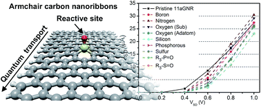
Fig. 4 depicts the current–voltage (IV) curves of both 8- and 11-aGNRs. As observed from Fig. 4(a), the turn on voltage for the undoped 11-aGNRs is ∼0.2 V, while doped systems does not exhibit a significant current until 0.4 V. Afterwards, at ∼0.8 V, N-, O(sub)- exhibit larger current than the undoped 11-aGNR, and later on, other doped systems, such as B- and S- exhibit comparable transport properties to the undoped nanoribbons, similar results have been reported for B- and N-doped nanocarbons.28,53 However, this is not the case when the functionalization is performed at the nanoribbon's edge. As observed from Fig. 4(b), in most cases the edge-doped 11-aGNRs exhibit inferior performance than their inside-doped counterparts, except for the amide (R2–NH) doped system. These results can be understood by examining their transmission functions (Fig. 3(a) and (b)), where lower transmission coefficients are presented in edge-doped systems caused by the existence of highly localized states, and thus lower current is achieved.


image file: c5ra25278d-f4.tif
Fig. 4 Electrical current (ISD) as a function of the applied voltage (VSD) of (a and b) 11-aGNRs and (c and d) 8-aGNRs.

The narrow 8-aGNRs seems to be also significantly affected even when the functionalization is performed within the ribbon lattice. Interestingly, B- and N-doped 8-aGNRs exhibit larger electrical current than the undoped case, following the trend previously observed for 11-aGNRs. However, the rest of the dopants significantly deteriorate the transport properties almost independently of the dopant position. These results suggest that wider graphene nanoribbons or graphene sheets could be functionalized at the inner sections in order to obtain improved chemical reactivity and excellent electron transport properties. Such characteristics are highly desirable in fuel cells,21,33,54 where doped graphene is used as a catalyst support or as a metal-free catalyst.

Finally, it is important to mention that other aGNRs from the 3p and 3p + 1 families might exhibit similar trends, where the inside-doping enhance the electron transport more than the edge-doping case.

We expanded the study to include the 7- and 10-aGNR (3p + 1), and the 9- and 12-aGNR (3p), where just two doping configurations are studied, P- (inside-doping) and R2–PH (edge-doping), the results are shown in Fig. S7. These nanoribbons exhibit larger band gap than the 3p + 2 family, and the introduction of phosphorous (inside or edge) results in enhanced electron transport when compared with the pristine case, contrary to the 3p + 2 family, at least for low applied voltages. However, the inside doping (P-) exhibit better transport characteristics than the edge case, especially for narrow ribbons, which is in line with the observed trend for 3p + 2 nanoribbons. A similar trend has been observed on doped single-walled carbon nanotubes (SWCNTs), where the electron transport properties of semiconductor SWCNTs are benefited from doping,55 but metallic SWCNTs give deteriorated transport properties.48

Conclusions

The electronic, structural, and transport properties of doped and functionalizedarmchair nanoribbons were studied using first principles calculations. We demonstrated that the incorporation of dopants (boron, nitrogen, oxygen, silicon, phosphorus, sulfur) and functional groups (borane, amine, hydroxyl, thiol, silane, silene, phosphine, phosphorane) into the nanoribbon lattice provides interesting electronic and transport properties that could be useful in the fabrication of sensors, catalysts or other electronic devices. We found that the nanoribbon's width and the dopant position strongly influence the overall transport properties, being possible to introduce different dopants without significantly compromise the transport characteristics while retaining the chemical reactivity that characterize these systems. Our results revealed that for 3p + 2 family of armchair graphene nanoribbons the edge doping act as a stronger scattering site when compared to the inside doping, mainly due the creation of diverse flat bands that belong to edge states, and do not contribute to the conduction. The present study provides relevant insight related to the role of the chemical doping on the physical and chemical properties of semiconductor graphene nanoribbons and could help to understand present and future experimental data obtained from doped carbon nanoribbons. However, even more theoretical studies are necessary since open questions regarding the role of doping concentration and number of graphene layers within the nanoribbons are not totally understood.

Acknowledgements

This work was supported in part by CONACYT-México grant 60218-F1 (FLU). EGE thanks to the Artificial Leaf Project Umeå (K&A Wallenberg Foundation) and the Ångpanneföreningen's Foundation (14-541). The theoretical simulations were performed on resources provided by the Swedish National Infrastructure for Computing (SNIC) at the High Performance Computing Center North (HPC2N).

Notes and references

  1. K. S. Novoselov, A. K. Geim, S. V. Morozov, D. Jiang, M. I. Katsnelson, I. V. Grigorieva, S. V. Dubonos and A. A. Firsov, Nature, 2005, 438, 197–200 CrossRef CAS PubMed.
  2. C. Berger, Z. Song, T. Li, X. Li, A. Y. Ogbazghi, R. Feng, Z. Dai, A. N. Marchenkov, E. H. Conrad, P. N. First and W. A. de Heer, J. Phys. Chem. B, 2004, 108, 19912–19916 CrossRef CAS.
  3. A. Reina, X. Jia, J. Ho, D. Nezich, H. Son, V. Bulovic, M. S. Dresselhaus and J. Kong, Nano Lett., 2009, 9, 30–35 CrossRef CAS PubMed.
  4. Z. Sun, Z. Yan, J. Yao, E. Beitler, Y. Zhu and J. M. Tour, Nature, 2010, 468, 549–552 CrossRef CAS PubMed.
  5. J. Cai, P. Ruffieux, R. Jaafar, M. Bieri, T. Braun, S. Blankenburg, M. Muoth, A. P. Seitsonen, M. Saleh, X. Feng, K. Mullen and R. Fasel, Nature, 2010, 466, 470–473 CrossRef CAS PubMed.
  6. A. K. Geim and K. S. Novoselov, Nat. Mater., 2007, 6, 183–191 CrossRef CAS PubMed.
  7. A. H. Castro Neto, F. Guinea, N. M. R. Peres, K. S. Novoselov and A. K. Geim, Rev. Mod. Phys., 2009, 81, 109–162 CrossRef CAS.
  8. K. Nakada, M. Fujita, G. Dresselhaus and M. S. Dresselhaus, Phys. Rev. B: Condens. Matter Mater. Phys., 1996, 54, 17954–17961 CrossRef CAS.
  9. Y.-W. Son, M. L. Cohen and S. G. Louie, Nature, 2006, 444, 347–349 CrossRef CAS PubMed.
  10. L. Tapaszto, G. Dobrik, P. Lambin and L. P. Biro, Nat. Nanotechnol., 2008, 3, 397–401 CrossRef CAS PubMed.
  11. B. G. Sumpter, V. Meunier, J. M. Romo-Herrera, E. Cruz-Silva, D. A. Cullen, H. Terrones, D. J. Smith and M. Terrones, ACS Nano, 2007, 1, 369–375 CrossRef CAS PubMed.
  12. J. M. Romo-Herrera, B. G. Sumpter, D. A. Cullen, H. Terrones, E. Cruz-Silva, D. J. Smith, V. Meunier and M. Terrones, Angew. Chem., Int. Ed., 2008, 47, 2948–2953 CrossRef CAS PubMed.
  13. J. Ortiz-Medina, et al., Adv. Funct. Mater., 2013, 23, 3755–3762 CrossRef CAS.
  14. D. Long, W. Li, L. Ling, J. Miyawaki, I. Mochida and S.-H. Yoon, Langmuir, 2010, 26, 16096–16102 CrossRef CAS PubMed.
  15. D. Deng, X. Pan, L. Yu, Y. Cui, Y. Jiang, J. Qi, W.-X. Li, Q. Fu, X. Ma, Q. Xue, G. Sun and X. Bao, Chem. Mater., 2011, 23, 1188–1193 CrossRef CAS.
  16. Z. Jin, J. Yao, C. Kittrell and J. M. Tour, ACS Nano, 2011, 5, 4112–4117 CrossRef CAS PubMed.
  17. N. Soin, S. Sinha Roy, S. Roy, K. S. Hazra, D. S. Misra, T. H. Lim, C. J. Hetherington and J. A. McLaughlin, J. Phys. Chem. C, 2011, 115, 5366–5372 CAS.
  18. A. L. M. Reddy, A. Srivastava, S. R. Gowda, H. Gullapalli, M. Dubey and P. M. Ajayan, ACS Nano, 2010, 4, 6337–6342 CrossRef CAS PubMed.
  19. T. Sharifi, M. Valvo, E. Gracia-Espino, R. Sandström, K. Edström and T. Wågberg, J. Power Sources, 2015, 279, 581–592 CrossRef CAS.
  20. X. Wang, L. Zhi and K. Müllen, Nano Lett., 2008, 8, 323–327 CrossRef CAS PubMed.
  21. L. Qu, Y. Liu, J.-B. Baek and L. Dai, ACS Nano, 2010, 4, 1321–1326 CrossRef CAS PubMed.
  22. F. Cervantes-Sodi, G. Csányi, S. Piscanec and A. C. Ferrari, Phys. Rev. B: Condens. Matter Mater. Phys., 2008, 77, 165427 CrossRef.
  23. M. Wu, C. Cao and J. Z. Jiang, Nanotechnology, 2010, 21, 505202 CrossRef CAS PubMed.
  24. B. Biel, F. Triozon, X. Blase and S. Roche, Nano Lett., 2009, 9, 2725–2729 CrossRef CAS PubMed.
  25. Z. Wang, H. Hu and H. Zeng, Appl. Phys. Lett., 2010, 96, 243110 CrossRef.
  26. E. Cruz-Silva, Z. M. Barnett, B. G. Sumpter and V. Meunier, Phys. Rev. B: Condens. Matter Mater. Phys., 2011, 83, 155445 CrossRef.
  27. N. Yasutaka, Y. Takashi, A. Fumihiko, Y. Yuichi, M. Hisao, K. Akihiro and S. Tadashi, Jpn. J. Appl. Phys., 2015, 54, 015101 CrossRef.
  28. P. S. Satyendra Singh Chauhan and A. K. Shrivastava, Appl. Nanosci., 2014, 4, 461–467 CrossRef.
  29. S. S. Yu, W. T. Zheng, Q. B. Wen and Q. Jiang, Carbon, 2008, 46, 537–543 CrossRef CAS.
  30. H. Zeng, J. Zhao, J. Wei, D. Xu and J. P. Leburton, Comput. Mater. Sci., 2012, 60, 234–238 CrossRef CAS.
  31. T. B. Martins, R. H. Miwa, A. J. R. da Silva and A. Fazzio, Phys. Rev. Lett., 2007, 98, 196803 CrossRef CAS PubMed.
  32. B. Biel, X. Blase, F. Triozon and S. Roche, Phys. Rev. Lett., 2009, 102, 096803 CrossRef PubMed.
  33. X.-K. Kong, C.-L. Chen and Q.-W. Chen, Chem. Soc. Rev., 2014, 43, 2841–2857 RSC.
  34. J. Taylor, H. Guo and J. Wang, Phys. Rev. B: Condens. Matter Mater. Phys., 2001, 63, 245407 CrossRef.
  35. P. Hohenberg and W. Kohn, Phys. Rev., 1964, 136, B864–B871 CrossRef.
  36. W. Kohn and L. J. Sham, Phys. Rev., 1965, 140, A1133–A1138 CrossRef.
  37. J. P. Perdew, A. Ruzsinszky, G. I. Csonka, O. A. Vydrov, G. E. Scuseria, L. A. Constantin, X. Zhou and K. Burke, Phys. Rev. Lett., 2008, 100, 136406 CrossRef PubMed.
  38. M. S. José, A. Emilio, D. G. Julian, G. Alberto, J. Javier, O. Pablo and S.-P. Daniel, J. Phys.: Condens. Matter, 2002, 14, 2745 CrossRef.
  39. J. Junquera, Ó. Paz, D. Sánchez-Portal and E. Artacho, Phys. Rev. B: Condens. Matter Mater. Phys., 2001, 64, 235111 CrossRef.
  40. N. Troullier and J. L. Martins, Phys. Rev. B: Condens. Matter Mater. Phys., 1991, 43, 1993–2006 CrossRef CAS.
  41. L. Kleinman and D. M. Bylander, Phys. Rev. Lett., 1982, 48, 1425–1428 CrossRef CAS.
  42. V. Barone, O. Hod and G. E. Scuseria, Nano Lett., 2006, 6, 2748–2754 CrossRef CAS PubMed.
  43. M. Brandbyge, J.-L. Mozos, P. Ordejón, J. Taylor and K. Stokbro, Phys. Rev. B: Condens. Matter Mater. Phys., 2002, 65, 165401 CrossRef.
  44. K. Stokbro, J. Taylor, M. Brandbyge and P. OrdejÓN, Ann. N. Y. Acad. Sci., 2003, 1006, 212–226 CrossRef CAS PubMed.
  45. M. Topsakal, V. M. K. Bagci and S. Ciraci, Phys. Rev. B: Condens. Matter Mater. Phys., 2010, 81, 205437 CrossRef.
  46. Y.-W. Son, M. L. Cohen and S. G. Louie, Phys. Rev. Lett., 2006, 97, 216803 CrossRef PubMed.
  47. Z. F. Wang, Q. Li, H. Zheng, H. Ren, H. Su, Q. W. Shi and J. Chen, Phys. Rev. B: Condens. Matter Mater. Phys., 2007, 75, 113406 CrossRef.
  48. E. Cruz-Silva, F. López-Urías, E. Muñoz-Sandoval, B. G. Sumpter, H. Terrones, J.-C. Charlier, V. Meunier and M. Terrones, ACS Nano, 2009, 3, 1913–1921 CrossRef CAS PubMed.
  49. J. Dai, J. Yuan and P. Giannozzi, Appl. Phys. Lett., 2009, 95, 232105 CrossRef.
  50. L. N. Chen, Solid State Commun., 2014, 191, 59–65 CrossRef CAS.
  51. K. Sawada, F. Ishii and M. Saito, J. Phys. Soc. Jpn., 2011, 80, 044712 CrossRef.
  52. Y. Li, Z. Zhou, P. Shen and Z. Chen, ACS Nano, 2009, 3, 1952–1958 CrossRef CAS PubMed.
  53. C.-C. Kaun, B. Larade, H. Mehrez, J. Taylor and H. Guo, Phys. Rev. B: Condens. Matter Mater. Phys., 2002, 65, 205416 CrossRef.
  54. E. Gracia-Espino, X. Jia and T. Wågberg, J. Phys. Chem. C, 2014, 118, 2804–2811 CAS.
  55. J. Wei, H. Hu, H. Zeng, Z. Zhou, W. Yang and P. Peng, Phys. E, 2008, 40, 462–466 CrossRef CAS.

Footnote

Electronic supplementary information (ESI) available. See DOI: 10.1039/c5ra25278d

This journal is © The Royal Society of Chemistry 2016
Click here to see how this site uses Cookies. View our privacy policy here.