
Oxidized nitinol substrate for interference enhanced Raman scattering of monolayer graphene†
Irfan Haider Abidia,
Aldrine Abenoja Caganga,
Abhishek Tyagia,
Muhammad Adil Riaza,
Ruizhe Wua,
Qingping Sunb and
Zhengtang Luo*a
aDepartment of Chemical and Biomolecular Engineering, Hong Kong University of Science and Technology, Clear Water Bay, Kowloon, Hong Kong. E-mail: keztluo@ust.hk
bDepartment of Mechanical and Aerospace Engineering, Hong Kong University of Science and Technology, Clear Water Bay, Kowloon, Hong Kong
First published on 12th January 2016
Abstract
We demonstrate the preparation of a controllable and reproducible active substrate for surface enhanced Raman scattering (SERS) using a facile oxidation method that allows us to obtain a titanium oxide (TiO2) capping layer with the desired thickness on nickel–titanium alloy (NiTi). The carefully tuned oxide layer, which is obtained by controlling the annealing time, exhibits the enhancement of the 2D band intensity of graphene up to ∼50 times in comparison to bare nitinol. The dependence of Raman enhancement upon the oxide thickness can be explained by the interference enhanced Raman scattering (IERS) process, and fitted to a multi reflection model (MRM) of the Raman scattering of graphene on a layered structure. Thus our results provide a facile method to enhance Raman signals of graphene by tuning the thickness of the oxide layer at all three lasers (514 nm, 633 nm and 785 nm). The present method can be adapted to exploit the recent advances in molecular vibration study and biomolecular detection due to the versatility of the proposed substrate.
Introduction
Surface enhanced Raman scattering (SERS) is a widely practiced technique used to enhance the Raman intensity of molecules. Normally the enhancement mechanism includes (1) electromagnetic enhancement (EME) which utilizes the plasmonic effect from metals such as Au, Ag and their nanostructures, and (2) chemical enhancement (CE) which is introduced by the change of the electronic state due to absorption.1,2 The chemical enhancement mechanism provides an appreciable magnitude of enhancement of 10 to 102, while the electromagnetic mechanism enhances the Raman intensity by a factor much larger than 106. Self-assembly of colloidal particles is a mature approach to create excellent SERS platforms and allows ultrasensitive SERS capabilities.3,4 However, difficulties in obtaining monodispersed colloids for reproducible results has hindered the large-scale application of this method. Recently, plasmon-free semiconducting substrates such as titanium oxide (TiO2) have been reported to exhibit considerable SERS enhancement attributed to molecule adsorption on its surface which modulates the TiO2-based nanostructures5–8 allowing them to be successfully employed for such purposes.6,9 Accordingly, these nanoparticles and nanostructures have become some of the most promising candidates for SERS due to their many advantages such as low cost, stability, biocompatibility and versatility in the fields of catalysis, analytical chemistry, electrochemistry and biomolecular sensing applications.10–12On the other hand, graphene has been known as wonder material and offers a great potential for electronic devices applications due to its unique electronic characteristics such as high carrier mobility, ballistic transport at ambient conditions and anomalous quantum Hall effect.13–15 Unfortunately, ordinary substrates used for graphene characterization exhibit very weak Raman signals, and even on some of substrates monolayer graphene is undetectable.1 The effect of substrates on the Raman features of graphene have been deeply investigated and reported.16,17 For instance, the Raman signal of graphene can be intensified by ∼102 times owing to the local-field plasmonic effect in the vicinity of noble metal nanoparticles or their nanostructures on Si/SiO2 substrate.18–22 On the contrary, silicon substrates with a 300 nm thick capping layer of SiO2 have been commonly utilized to enhance the Raman signal of graphene by 30 times23,24 as well as to make graphene visible with optimal contrast under white light.25 This kind of layer structured substrate enables the interference-enhanced Raman scattering (IERS) phenomenon26,27 which is being taken advantage of to enhance Raman signals of very thin film samples.28,29 In this technique, the thickness of the oxide layer is adjusted to arrange interference conditions for the absorption of all the incident energy within the structure, which is then eventually added to the emitted Raman scattered radiations yielding a significant gain in the measured Raman signals.26,30 However, Si/SiO2 substrates provide limitations to characterize graphene at 785 nm laser due to huge fluorescence background of Si/SiO2.31,32 Therefore, a robust, inexpensive and a substrate easy to fabricate is inevitable for Raman enhancement of monolayer graphene.
In this work, we developed a facile method to synthesize an overlayer structure that can provide an oxide surface for Raman enhancement. This SERS active substrate is composed of a TiO2 capping layer that was synthesized on nickel–titanium (NiTi or nitinol) alloy. NiTi is a suitable substrate for this study due to its tunable thickness by controlled annealing. Furthermore, the purpose of selecting nitinol as substrate is owing to the great importance of this alloy in biomedical applications. Recently, graphene growth on NiTi showed enhanced bioactive surfaces as well as protection form Ni release.33,34 Therefore, graphene on NiTi surface could be very interesting combination to study. Moreover, 2D structure of graphene sheet also provides ideal platform to probe the SERS effect of our proposed substrate. Therefore, we used graphene as an analyte to probe the SERS effect in our study. We observe that the Raman intensity of graphene is strongly dependent on the thickness of TiO2 similar to previous reports of their SiO2 counterparts.24,30 Both 2D and G bands have shown substantial intensity enhancements for nanometer-sized TiO2 thickness at all three different excitation laser energies employed in this work which are 514 nm, 633 nm and 785 nm. The sensitivity of enhancement can be tuned by adjusting the thickness of the capping layer for a particular excitation laser. Such intensity dependence can be explained with an interference enhanced Raman scattering (IERS) phenomenon and multi reflection model.28,35 We extended our observation of the Raman enhancements to other analytes using Methylene Blue (MB) on the prepared substrate as a model which also demonstrated a substantial increase in signals. In addition, the substrate prepared by this method could also be useful for studies of 2D materials other than graphene with low Raman cross-section. The outcome of the study paves the way towards an alternative substrate for the fundamental as well as applied research of limelight graphene, and other molecules significant for sensing applications, with advantages of being inexpensive, versatile and easy to fabricate.
Experimental procedures
Synthesis of oxide layer on NiTi alloy
NiTi alloy sheet (300 μm thickness) was cut into 10 mm × 10 mm pieces, mechanically polished with series of emery paper and polishing cloth to obtain a smooth surface. The polished samples were ultrasonically cleaned in deionized water, ethanol and IPA to remove any contaminants and dried with N2 gun. The NiTi samples were loaded in tube furnace with sliding chamber to control the fast heating and cooling rate. The samples were annealed at 540 °C (optimized) at atmospheric pressure with various sharp time intervals such as 2, 3.5, 5, 7, 10 and 20 minutes with abrupt heating and cooling.Graphene growth by chemical vapor deposition and transfer
Continuous monolayer graphene was grown by CVD method described in detail in our previous work.36 Briefly, copper foil was chemically polished in diluted aqueous FeCl3 etchant, then rinsed with DI water and dried under flow of N2. The Cu foil was then placed in quartz tube furnace and heated to 1050 °C under the flow of Ar (350 sccm) and H2 (21 sccm) and annealed for 30 minutes. Then CH4 gas as carbon source was introduced with flow rate of 15 sccm for 30 minutes. After that, the system was rapidly cooled down by switching off and sliding off the furnace. After CVD growth on Cu foil, transfer of graphene was carried out through wet etching process. A 300 nm thick PMMA coating was applied on the Cu/graphene by spin coating at 3000 rpm for 40 s followed by curing at 160 °C for 5 minutes. Transparent graphene/PMMA film was attained by etching away Cu beneath using etchant (10 g FeCl3, 10 ml HCl and 200 ml DI water), subsequently rinsing with diluted HCl solution and DI water for 30 minutes to remove etchant contaminants. Thereafter, the floating graphene/PMMA film was retained on the substrate (oxidized NiTi). Finally, the PMMA layer was dissolved away in boiling acetone, and we get graphene on our corresponding substrates.Characterization
The evolution of oxide layer (TiO2) with annealing time was characterized by obtaining X-ray diffraction pattern through high resolution X-ray diffraction system (PW1825 Philips), operated in thin film mode (Cu Kα radiation, 40 kV, 30 mA, grazing incidence at 1°).In order to measure the TiO2 capping layer thickness, time-of-flight secondary ion mass spectrometer (ION-TOF GmbH) was employed using Cs as primary ions source, 3 keV sputtering energy. The reflectance spectra of all substrates were acquired through UV-Vis spectrophotometer (Lambda 20, Perkin Elmer) with 1 nm resolution.
The graphene transferred on oxidized substrate was visualized with optical microscope (LEICA DFC 290). Raman analysis were performed using an InVia micro Raman system (Renishaw) equipped with three excitation laser sources; Ar+ ion laser 514.5 nm (∼514 nm), He–Ne laser 632.8 (∼633 nm), diode laser 785 nm. A 50× objective lens was used to focus the laser beam. The laser power at the sample surface was ∼4 mW. For SERS study of MB, the prepared substrates were incubated in 10−4 M MB container for 1 h, subsequently washed with DI water and dried in N2 atmosphere. For comparative study, all the parameters and conditions for one set of samples under one particular laser line, were kept constant. The intensities of peaks were acquired by fitting the spectra with Lorentzian function.
Results and discussion
The present strategy to prepare substrate for surface enhanced Raman scattering (SERS) is TiO2 capping layer with controlled thickness. As described in the Experimental section, the NiTi alloy was annealed at 540 °C for different time intervals in atmospheric conditions. Fig. 1a shows the photographs taken under white light of seven substrates fabricated at different annealing time of 0, 2, 3.5, 5, 7, 10 and 20 minutes. The substrates exhibit a variety of colors that is very similar to the dispersion of colors by prism, allude to us that different annealing time lead to varied overlayer thickness. The appearance of colors also indicates indirectly the enhanced interaction of light with the structure, showing their potential use for Raman enhancement. We then identified the composition and thickness of overlayer through secondary ions mass spectroscopy (SIMS), shown in Fig. 1b. Since SIMS mechanism follows the sputtering of ions on the top layer of the specimen to get the sample composition in depth. Therefore, we get information of relative ionic composition into the prescribed depth of the specimens. Here the intersecting point of TiO2 and Ni spectra (pointing with arrows) was identified with as an interface between layers of TiO2 (top) and NiTi (bottom), and depth at that point determines the thickness of TiO2 capping layer. Since at the top of the specimen Ni ions were absent as NiTi covered with oxide layer, but as going through the depth we reach the interface where we get stronger Ni signals. The SIMS analysis vindicate that the thickness of oxide can be regulated with the annealing time. Herein, we denote our samples as T-0, T-30, T-44, T-54, T-65, T-79 and T-139, corresponding to the thickness (nm) of TiO2 capping layer with 0, 2, 3.5, 5, 7, 10 and 20 minutes of annealing time, respectively.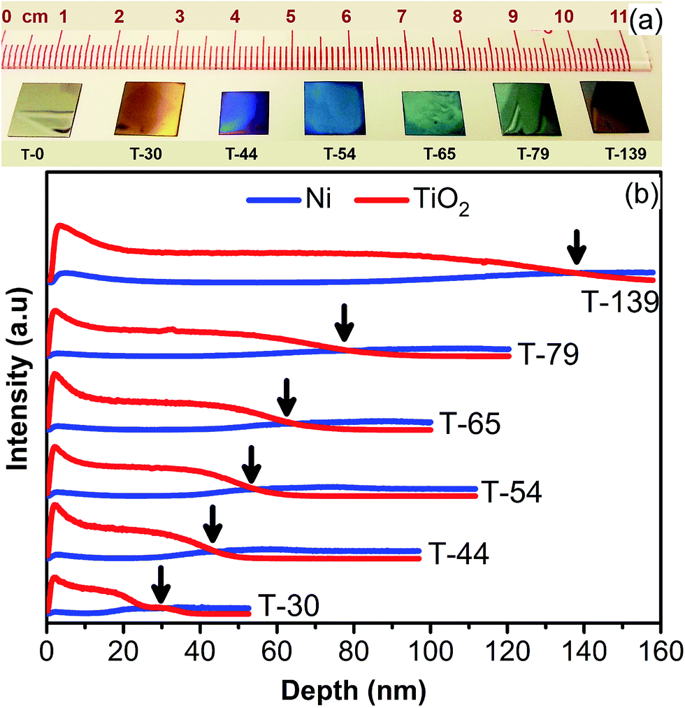 | ||
| Fig. 1 Depth analysis from Secondary Ions Mass Spectroscopy (SIMS). (a) A photograph of substrates synthesized with annealing time 0, 2, 3.5, 5, 7, 10 and 20 minutes (from left to right). (b) SIMS depth profile of various substrates. The intersecting point of TiO2 and Ni has been taken as an interface between oxide layer and NiTi substrate to evaluate the thickness represented with arrows. | ||
The composition of the capping layers is further corroborated by X-ray diffraction (XRD). Fig. 2a illustrates the X-ray diffraction (XRD) analysis of NiTi alloy of the same samples. For sample without annealing, i.e. sample T-0, no TiO2 peak were observed, however, rutile TiO2 characteristic 2θ peaks appeared at 27.4°, 54.3°, and 56.6°, respectively corresponding to R(110), R(211) and R(220), with peak intensity increasing as a function of annealing time. Interestingly, no nickel oxides, such as NiO or Ni2O3, were observed.
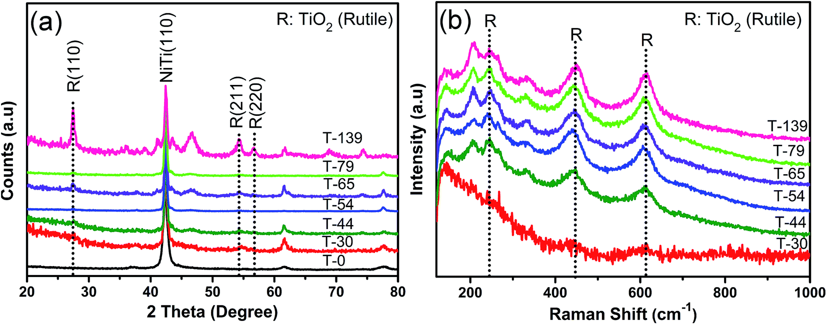 | ||
| Fig. 2 Characterization of oxidized nitinol substrates. (a) XRD spectra reflecting evolution of TiO2 (rutile) peak with annealing time. (b) Raman spectra of substrates of annealed NiTi samples exhibiting the characteristic Raman bands of TiO2 (rutile). | ||
Further evidence for the formation of TiO2 capping layer is confirmed with Raman spectra of the annealed samples, shown in Fig. 2b, in which, the typical TiO2 (rutile) Raman peaks at 446 cm−1 and 611 cm−1 become more prominent, and gradually evolved as function of annealing time, without observation of nickel oxide phases. Such evidence indicates that our method here facilitated preferential growth of TiO2 capping layer on the surface of NiTi alloy, but avoids the formation of NiO or Ni2O3. Such observation is consistent with the fact that titanium has higher affinity with oxygen than nickel, with the lower formation free energies, which are −759 and −147 kJ mol−1 for TiO2 and NiO, respectively.37 XRD and Raman spectra reflect the preferential growth of rutile phase of TiO2 rather than other anatase or brookite phase, which is attributed to the annealing temperature employed in this work i.e., 540 °C. As reported previously, oxidation of NiTi in air results in anatase phase at 400–450 °C, while at temperature >450 °C, rutile phase start forming.37,38 In accordance to this, we found mostly rutile phase, however we cannot ruled out the presence of slight amount of anatase or brookite phase at present conditions. Moreover, the effect of crystalline phase; rutile, anatase or brookite on Raman enhancement is not very obvious.6,39 Therefore, we choose not to explore this aspect in our present work.
To study the Raman enhancement effect of the prepared oxides/nitinol substrate, we first synthesized the graphene monolayer film through CVD process explained in Experimental section. The graphene/Cu substrate coated with 300 nm PMMA layer, subsequently Cu etched away in FeCl3 solution. The PMMA/graphene stacked then washed with DI water and scooped up on the substrates (T-0, T-139 etc.). Finally, PMMA is removed with boiling acetone bath and subsequently substrates washed with DI water, ethanol and dried with N2 gun. Fig. 3a–c illustrates the Raman spectra of graphene on aforementioned substrates using 514 nm, 633 nm and 785 nm excitation wavelength respectively. Normally for Raman spectra of graphene, three distinctive bands are identified, i.e. D band (1350 cm−1); G band (∼1580 cm−1) and the 2D band (∼2686 cm−1).40,41 G band originates from in-plane vibrations of sp2 carbon atoms resulting in E2g phonon emission, with intensity very sensitive to number of layers.41,42 On the other hand, 2D band is from the double resonant Raman scattering with two phonon emissions process.26,40 The shape of the 2D band reflects the number of layers of graphene, for instance 2D band splits into four peaks for a bilayer graphene and a single peak for monolayer graphene.16,43 D band appears from breathing modes of six-atom rings, accounts for the defects in graphene structure. The frequencies of 2D band (also known as G′ band) and D band depend on the excitation energy of incident laser.32,42 Moreover, the intensity ratio of 2D to G bands has great importance to predict the number of layers of graphene irrespective of the experimental conditions as generally it is accepted that ratio remains to be unaffected to the external factors.23,41 In Fig. 3a–c, we can see all of the spectra exhibited I2D/IG ratio greater than 1, typical for monolayer graphene, indicating the high quality of our CVD graphene. In fact, monolayer graphene provides distinguishable contrast under optical microscope on some of substrates especially for i.e., T-30, T-44. While for the other substrates contrast is discernable under microscope but not an appropriate contrast with image taken with LEICA Image analyzer software. Moreover, the 2D peak has also shown a progressively red shift as a function of laser wavelength, regardless of the excitation laser energy. For instance using T-79 sample, the 2D peak are at 2681 cm−1, 2633 cm−1 and 2589 cm−1 using excitation laser 514 nm, 633 nm and 785 nm, respectively, consistent with reported red shift of 100 cm−1 eV−1.32 This suggests that the transferred graphene on this substrate are similar to those on other commonly used oxide substrates.
 | ||
| Fig. 3 Comparison of Raman enhancement of graphene on different substrate synthesized in this work, at three wavelengths of laser used. It can be observed that Raman intensity is a function of TiO2 thickness (a) 514 nm laser, it appears that Raman signals of graphene 2D band was strongest in case of T-44 as compared to other substrates and a significant enhancement can be observe as compare to polished NiTi substrate i.e., T-0. (b) 633 nm laser, reveals that 2D bands has strongest Raman signal at T-54 substrate. (c) 785 nm laser, reflects that the maximum enhancement of 2D band shown by T-79 substrate. In all set of Raman spectra, measurement conditions such as laser power, exposure time and collecting lens kept the same. (d) Raman intensity of 2D band of graphene at 30 random spots at (i) T-44@514 nm (ii) T-54@633 nm (iii) T-79@785 nm. | ||
The enhancement of the Raman intensity is clearly observed when TiO2 capping layer is grown on the nitinol. Without oxide capping layer, the Raman signals is very weak, as shown in Fig. 3a–c. However, the growth of TiO2 capping layer significantly enhances the Raman intensity, with a magnitude depending on the oxide thickness and excitation laser energy. As shown in Fig. 3a under 514 nm laser excitation, the 2D peak intensity increases initially with TiO2 thickness (from T-0 to T-44), then start decreasing with further increase in TiO2 thickness to minimum on T-79 (79 nm TiO2) and then again enhances on T-139 (∼139 nm TiO2). The maximum enhancement of 2D-band was ∼35 times on T-44 (∼44 nm TiO2) substrate as compare to T-0 (bare NiTi), pointing with arrow in Fig. 3a. Similarly, Raman spectra collected at 633 nm laser, also showed variation of intensity enhancement with thickness of TiO2, but in contrast, here the maximum enhancement of 2D-band demonstrated by T-54 (54 nm TiO2) rather T-44 (Fig. 3b). The T-54 (pointing with arrow) has shown a substantial enhancement of ∼54 and ∼51 times for 2D and G bands, respectively, as compare to T-0 (bare NiTi). The Raman enhancement variation follows the similar trend while using 785 nm laser, shown in Fig. 3c, where the maximum enhancement for 2D band, exhibited by T-79 with enhancement factor of ∼44 times. Another, important observation is lack of high fluorescence background at 785 nm on all of the substrates. This provides advantage of proposed substrates to study Raman features of graphene at 785 nm over traditional SiO2/Si substrate. The Raman enhancement of monolayer graphene sheet was also very uniform rather patches, depicted as Raman mapping analysis, shown in Fig. S2.† The dependence of Raman enhancement on thickness of TiO2 is quite analogous to that observed in the case of SiO2/Si.24,35 Hence, through carefully analyzing the series of Raman spectra, we can realize the Raman intensity enhancement by tuning TiO2 capping layer thickness and excitation laser energy.
In addition to graphene, we performed SERS analysis for methylene blue (MB) as an analyte to evaluate the prospect of our proposed substrates for Raman enhancement. 10−4 M MB was used to adsorb molecules on T-54 substrate. Raman spectrum of 10−4 M MB@T-54 shows a substantial enhancement of Raman bands of MB, as shown in Fig. S3.† Raman spectrum of same analyte on SiO2/Si is also provided for comparison. These results reflect the great potential of these substrates for SERS and sensing applications.
To understand the mechanism of the Raman enhancement, we performed studies on the optical absorption. The reflectance spectra of various substrates depicted in Fig. 4a, has an immense importance to understand the dispersive behavior of enhancement at different wavelength of laser. The enhanced light–matter interaction is very essential for Raman intensity enhancement process, since it increases the probability of Raman scattering process and multiple laser scattering.7 The interaction of laser light depends on the reflectance (absorption) behavior of host structure, for instance, to greatly enhance the interaction, the structure should have minimum reflectance (maximum absorption) of incident laser light so that laser light can get more time span to interact with host structure, in other words more scattering opportunities in turns enhanced Raman signals. While analyzing the reflectance spectra of substrates (T-0 to T-139) shown in Fig. 4a, we can find dips and peaks in almost each of the spectra, which indirectly defines the Raman scattering behavior of corresponding substrate over the range of wavelength. The neck of the peak in the reflectance spectrum represent the point of minimum reflectance at that particular wavelength, which is favorable for the opportunity of maximum Raman scattering and enhancement of Raman intensity.7 The dotted lines represent the laser wavelengths utilized in this study i.e., 514 nm, 633 nm, and 785 nm. It can be observed that lasers 514 nm, 633 nm and 785 nm pinpoints at the neck of the peak in reflectance spectra of T-44, T-54 and T-79, respectively. While 514 nm and 633 nm lasers locate at almost the center of peak in the reflectance spectra of T-79 and T-139, respectively. These observations are in great accordance to the Raman spectra of all substrates discussed above, and explain the degree of Raman enhancement dispersion with three different laser energies. For example, in the case of 633 nm laser, T-54 had shown the maximum Raman enhancement for 2D band which can be attributed to the position of dip (neck of peak) in reflectance spectra (Fig. 4a), matches narrowly to the excitation laser wavelength, in contrast the excitation wavelength (633 nm) exist at the almost middle of the peak for T-79 which shows minimum Raman enhancement.
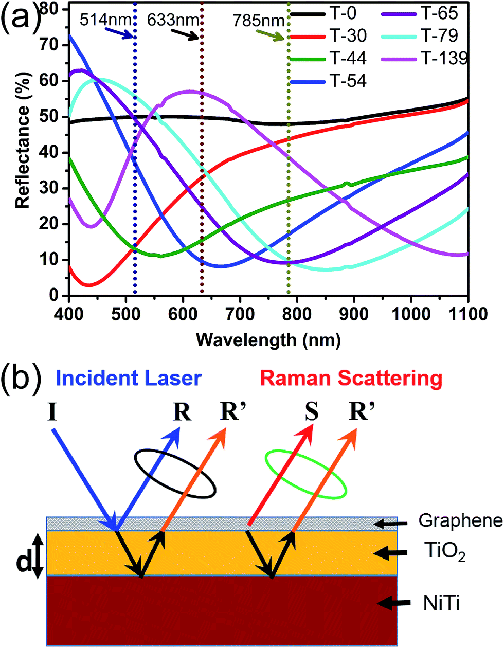 | ||
| Fig. 4 UV-Vis reflectance spectra of oxidized nitinol substrates. (a) All of the substrates have shown dip (neck of peak) in the reflectance spectra which corresponds to minimum reflection (maximum absorption) at that particular wavelength except T-0. (b) Schematic of the proposed layered structure to trigger interference enhanced Raman scattering (IERS) phenomenon. | ||
In addition, reflectance spectra also explain well the variation in colors of the corresponding substrates shown in Fig. 1a, the peaks are matches obviously with the colors. Moreover, monolayer graphene is visible and shown a great contrast on few of the substrates under white light, when observed with optical microscope (Fig. S1†). Consequently, we demonstrated that by carefully tuned the peak position of reflectance spectra through modulation of the TiO2 thickness, optimal Raman enhancement can be achieved at particular laser wavelength.
On the other hand, we propose that the Raman enhancement behavior of oxide layer is due to Interference enhanced Raman scattering (IERS). IERS is known as one of the mechanism to enhance the Raman intensity on layered structure. Fig. 4b shows the schematic of our proposed structure to trigger the IERS effect to enhance the Raman signal of graphene laying on it. In principle, when incident laser beam “I” hits the surface, partially reflected back from the top surface of TiO2 denoted as R, rest penetrates through the TiO2 layer with thickness “d” and reflected back from the interface TiO2/NiTi denoted as R′. Meanwhile, we also have Raman scattered radiations “S” from graphene which generates Raman signals. Now, there are two situations; (1) the reflected beam R′ interfere constructively with the top reflected beam R, which is negative to the Raman enhancement (2) the both reflected beam R′ and R interfere destructively, which will provide more time span to laser light to scatter through the structure. These multiple laser scattering through the structure enhanced significantly light–matter interaction, consequently there will more occasions of Raman scattering process resulting into enhanced Raman signals. In other words, the bottom reflected beam interfere constructively with Raman scattered beams S to enhance the resultant signals. However, the interference of light is a function of refractive index and thickness of capping oxide layer “d” and the wavelength of incident laser,28,35 but at particular wavelength and refractive index of TiO2, interference conditions can be modulated through tuning the thickness “d”. Hence, in order to get maximum Raman enhancement at some particular laser wavelength, the thickness of TiO2 is tuned to match condition for destructive interference between R and R′. Therefore, we assume that T-44, T-54 and T-79 substrates match the condition to enhance the Raman intensity at 514 nm, 633 nm and 785 nm lasers, respectively.
In order to validate our experimental findings and to explain the wavering enhancement behavior with TiO2 thickness, we did theoretical calculations using multireflection model (MRM) of the Raman scattering based on Fresnel's equations.26,44 The details of all the equations and parameters used can be found in ESI.† In MRM, the absorption and scattering processes are treated separately and expressed by two separate terms of net absorption and scattering on the course of multiple reflections inside graphene monolayer as well as TiO2 capping layer. Moreover, for narrow TiO2 capping layer thickness, the incident laser and Raman scattered light wavelengths are considered to be the same, similar to the earlier reports.24,45 The calculated values of intensity with TiO2, of both G and 2D bands at three different lasers are shown with solid fitting lines in Fig. 5a and b. It can be demonstrated from the Fig. 5a and b that our experimental and theoretical results are well in accordance almost at all laser wavelengths. It can be seen that the intensity of G (or 2D) shows oscillating behavior with thickness of TiO2, similar to the results obtained for SiO2/Si substrates.26,30 This oscillating behavior also represent the interference effect on Raman scattering of G and 2D bands of graphene.35 Furthermore, it is worth noticing that at higher wavelength of laser, the maxima for both G and 2D shifted towards thicker TiO2 capping layer. Henceforth, the thickness of the TiO2 capping layer can be tuned well to match the intensity maxima at some particular excitation wavelength as we demonstrated here. The proposed substrates are very useful for the Raman enhancement of graphene, and provides the benefit of being inexpensive and facile to synthesize. We believe that the Raman enhancement phenomena of synthesized substrates can be extended to other molecules and can be useful in analytical chemistry and biosensing applications.
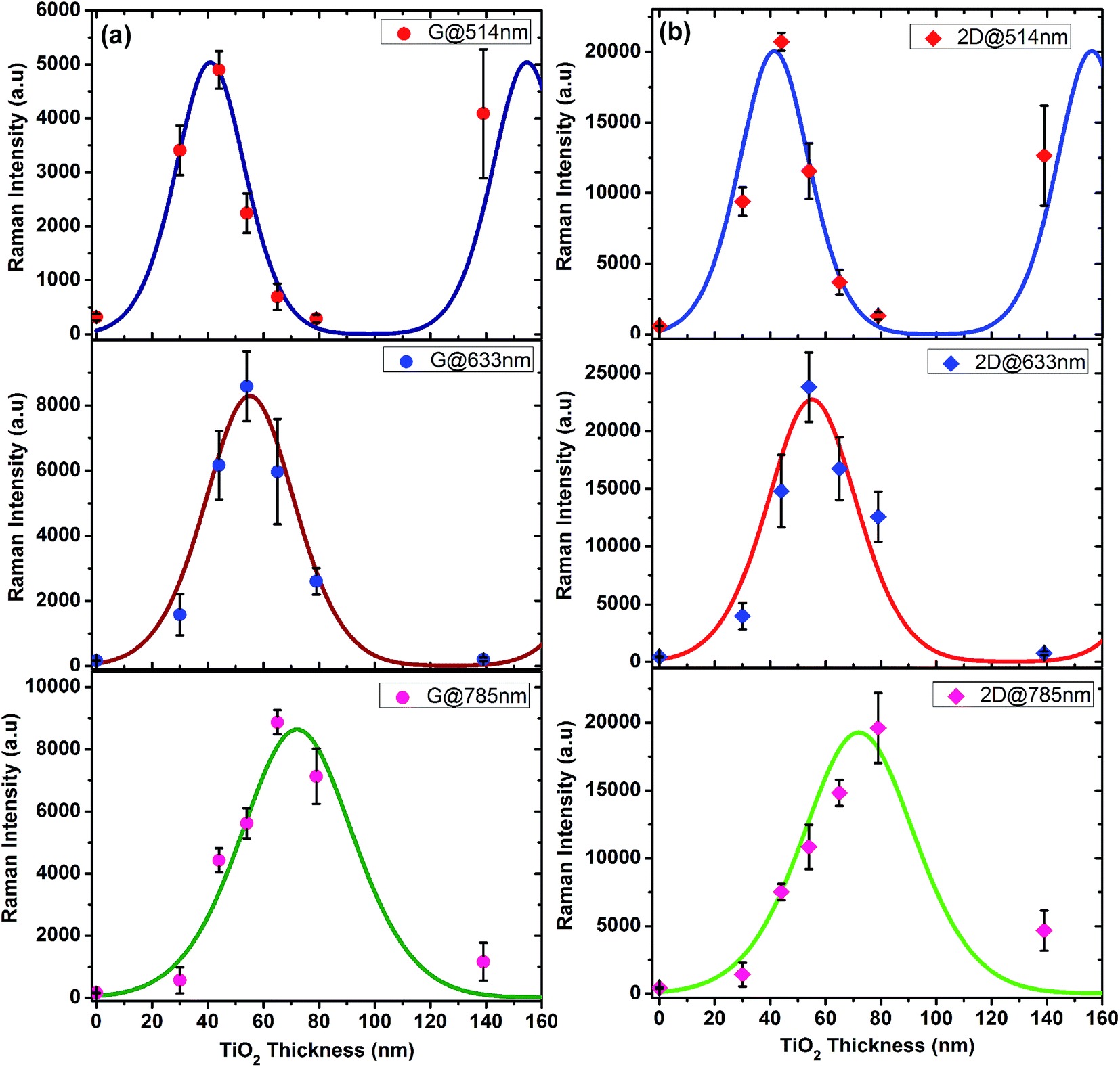 | ||
| Fig. 5 Raman intensities and fitting with multireflection model. The dots represent the experimental Raman intensities of (a) G band (b) 2D band of graphene with variation in TiO2 capping layer thickness. The experimental results are fitted (solid lines) with multireflection model. The intensities are oscillating with TiO2 thickness and experimental and theoretical results are in agreement. | ||
Conclusions
We proposed a facile method to synthesize TiO2 capping layer on nitinol substrate that can substantially enhance the Raman signal of graphene. It is demonstrated that the intensity of 2D and G bands of graphene is a strong function of TiO2 thickness, and Raman enhancement occurs due to Interference enhanced Raman scattering phenomenon. The extent of enhancement varies with the degree of constructive or destructive interference of incident and reflected/scattered laser light depending on TiO2 thickness. The intensity maxima also varies with excitation wavelength of laser, so that we can tune the thickness of TiO2 in order to match the conditions for the maximum enhancement. Finally, multireflection model justified theoretically our experimental findings in terms of multiple reflection and interference phenomena as both have shown consensus. The substrate presented here for Raman enhancement could be extremely useful for other biosensing and analytical applications as well by carefully exploiting the surface features.Acknowledgements
This project is supported by the Research Grant Council of Hong Kong SAR (Project number 623512 and DAG12EG05) and SFC/RGC Joint Research Scheme (Project number X-HKUST603/14). I. H. Abidi appreciate financial support from Higher Education Commission (HEC) of Pakistan. Moreover, we are thankful to Mr Yu Gao for his valuable suggestions. Technical assistance from the Materials Characterization and Preparation Facilities is greatly appreciated.Notes and references
- X. Fu, F. Bei, X. Wang, S. O'Brien and J. R. Lombardi, Nanoscale, 2010, 2, 1461–1466 RSC.
- K. Kneipp, H. Kneipp, I. Itzkan, R. R. Dasari and M. S. Feld, J. Phys.: Condens. Matter, 2002, 14, R597 CrossRef CAS.
- X. Li, H. Hu, D. Li, Z. Shen, Q. Xiong, S. Li and H. J. Fan, ACS Appl. Mater. Interfaces, 2012, 4, 2180–2185 CAS.
- D. M. Kuncicky, B. G. Prevo and O. D. Velev, J. Mater. Chem., 2006, 16, 1207–1211 RSC.
- X. Wang, W. Shi, G. She and L. Mu, Phys. Chem. Chem. Phys., 2012, 14, 5891–5901 RSC.
- D. Maznichenko, K. Venkatakrishnan and B. Tan, J. Phys. Chem. C, 2013, 117, 578–583 CAS.
- D. Qi, L. Lu, L. Wang and J. Zhang, J. Am. Chem. Soc., 2014, 136, 9886–9889 CrossRef CAS PubMed.
- H.-Y. Shin, E.-L. Shim, Y.-J. Choi, J.-H. Park and S. Yoon, Nanoscale, 2014, 6, 14622–14626 RSC.
- Y. Xie and Y. Meng, RSC Adv., 2014, 4, 41734–41743 RSC.
- A. Musumeci, D. Gosztola, T. Schiller, N. M. Dimitrijevic, V. Mujica, D. Martin and T. Rajh, J. Am. Chem. Soc., 2009, 131, 6040–6041 CrossRef CAS PubMed.
- L. Yang, X. Jiang, W. Ruan, B. Zhao, W. Xu and J. R. Lombardi, J. Phys. Chem. C, 2008, 112, 20095–20098 CAS.
- C. M. Girish, S. Iyer, K. Thankappan, V. V. D. Rani, G. S. Gowd, D. Menon, S. Nair and M. Koyakutty, J. Mater. Chem. B, 2014, 2, 989–998 RSC.
- K. S. Novoselov, A. K. Geim, S. Morozov, D. Jiang, Y. Zhang, S. Dubonos, I. Grigorieva and A. Firsov, Science, 2004, 306, 666–669 CrossRef CAS PubMed.
- K. S. Novoselov, Z. Jiang, Y. Zhang, S. V. Morozov, H. L. Stormer, U. Zeitler, J. C. Maan, G. S. Boebinger, P. Kim and A. K. Geim, Science, 2007, 315, 1379 CrossRef CAS PubMed.
- A. K. Geim and K. S. Novoselov, Nat. Mater., 2007, 6, 183–191 CrossRef CAS PubMed.
- Y. Y. Wang, Z. H. Ni, T. Yu, Z. X. Shen, H. M. Wang, Y. H. Wu, W. Chen and A. T. Shen Wee, J. Phys. Chem. C, 2008, 112, 10637–10640 CAS.
- I. Calizo, W. Bao, F. Miao, C. N. Lau and A. A. Balandin, Appl. Phys. Lett., 2007, 91, 201904 CrossRef.
- M. Kalbac, V. Vales and J. Vejpravova, RSC Adv., 2014, 4, 60929–60935 RSC.
- Y. Zhao, G. Chen, Y. Du, J. Xu, S. Wu, Y. Qu and Y. Zhu, Nanoscale, 2014, 6, 13754–13760 RSC.
- F. Schedin, E. Lidorikis, A. Lombardo, V. G. Kravets, A. K. Geim, A. N. Grigorenko, K. S. Novoselov and A. C. Ferrari, ACS Nano, 2010, 4, 5617–5626 CrossRef CAS PubMed.
- J. Lee, S. Shim, B. Kim and H. S. Shin, Chem.–Eur. J., 2011, 17, 2381–2387 CrossRef CAS PubMed.
- J. Lee, K. S. Novoselov and H. S. Shin, ACS Nano, 2011, 5, 608–612 CrossRef CAS PubMed.
- A. Gupta, G. Chen, P. Joshi, S. Tadigadapa and P. C. Eklund, Nano Lett., 2006, 6, 2667–2673 CrossRef CAS PubMed.
- Y. Y. Wang, Z. H. Ni, Z. X. Shen, H. M. Wang and Y. H. Wu, Appl. Phys. Lett., 2008, 92, 043121 CrossRef.
- A. Reina, H. Son, L. Jiao, B. Fan, M. S. Dresselhaus, Z. Liu and J. Kong, J. Phys. Chem. C, 2008, 112, 17741–17744 CAS.
- D. Yoon, H. Moon, Y.-W. Son, J. S. Choi, B. H. Park, Y. H. Cha, Y. D. Kim and H. Cheong, Phys. Rev. B: Condens. Matter Mater. Phys., 2009, 80, 125422 CrossRef.
- R. Nemanich, C. Tsai and G. Connell, Phys. Rev. Lett., 1980, 44, 273 CrossRef CAS.
- S. Gupta, G. Morell, R. S. Katiyar, J. R. Abelson, H. C. Jin and I. Balberg, J. Raman Spectrosc., 2001, 32, 23–25 CrossRef CAS.
- G. A. N. Connell, R. J. Nemanich and C. C. Tsai, Appl. Phys. Lett., 1980, 36, 31–33 CrossRef CAS.
- C. Liu, Y. Ma, W. Li and L. Dai, Appl. Phys. Lett., 2013, 103, 213103 CrossRef.
- P. Wang, D. Zhang, L. Zhang and Y. Fang, Chem. Phys. Lett., 2013, 556, 146–150 CrossRef CAS.
- L. M. Malard, M. A. Pimenta, G. Dresselhaus and M. S. Dresselhaus, Phys. Rep., 2009, 473, 51–87 CrossRef CAS.
- R. Podila, T. Moore, F. Alexis and A. M. Rao, RSC Adv., 2013, 3, 1660–1665 RSC.
- J. Li, G. Wang, H. Geng, H. Zhu, M. Zhang, Z. Di, X. Liu, P. K. Chu and X. Wang, ACS Appl. Mater. Interfaces, 2015, 7, 19876–19881 CAS.
- X. Ling and J. Zhang, J. Phys. Chem. C, 2011, 115, 2835–2840 CAS.
- L. Gan and Z. Luo, ACS Nano, 2013, 7, 9480–9488 CrossRef CAS PubMed.
- Y. W. Gu, B. Y. Tay, C. S. Lim and M. S. Yong, Appl. Surf. Sci., 2005, 252, 2038–2049 CrossRef CAS.
- K. S. Kim, K. K. Jee, W. C. Kim, W. Y. Jang and S. H. Han, Mater. Sci. Eng., A, 2008, 481–482, 658–661 CrossRef.
- T.-L. Guo, J.-G. Li, D.-H. Ping, X. Sun and Y. Sakka, ACS Appl. Mater. Interfaces, 2014, 6, 236–243 CAS.
- A. Ferrari, J. Meyer, V. Scardaci, C. Casiraghi, M. Lazzeri, F. Mauri, S. Piscanec, D. Jiang, K. Novoselov and S. Roth, Phys. Rev. Lett., 2006, 97, 187401 CrossRef CAS PubMed.
- D. Graf, F. Molitor, K. Ensslin, C. Stampfer, A. Jungen, C. Hierold and L. Wirtz, Nano Lett., 2007, 7, 238–242 CrossRef CAS PubMed.
- P. Klar, E. Lidorikis, A. Eckmann, I. Verzhbitskiy, A. Ferrari and C. Casiraghi, Phys. Rev. B: Condens. Matter Mater. Phys., 2013, 87, 205435 CrossRef.
- A. C. Ferrari and D. M. Basko, Nat. Nanotechnol., 2013, 8, 235–246 CrossRef CAS PubMed.
- J. W. Ager, D. K. Veirs and G. M. Rosenblatt, J. Chem. Phys., 1990, 92, 2067–2076 CrossRef CAS.
- Z. H. Ni, H. M. Wang, J. Kasim, H. M. Fan, T. Yu, Y. H. Wu, Y. P. Feng and Z. X. Shen, Nano Lett., 2007, 7, 2758–2763 CrossRef CAS PubMed.
Footnote |
| † Electronic supplementary information (ESI) available: Raman mapping and optical micrographs of graphene on various substrates, details of multireflection model are provided. See DOI: 10.1039/c5ra24842f |
| This journal is © The Royal Society of Chemistry 2016 |