
Electric, magnetic, piezoelectric and magnetoelectric studies of phase pure (BiFeO3–NaNbO3)–(P(VDF-TrFE)) nanocomposite films prepared by spin coating
Rehana P. Ummera,
Raneesh Bd,
Camille Thevenotef,
Didier Rouxelef,
Sabu Thomasbc and
Nandakumar Kalarikkal*ac
aSchool of Pure and Applied Physics, Mahatma Gandhi University, Kottayam, Kerala-686560, India. E-mail: nkkalarikkal@mgu.ac.in; Fax: +91-481-2731669; Tel: +91-944-7671962
bSchool of Chemical Sciences, Mahatma Gandhi University, Kottayam, Kerala-686560, India
cInternational and Inter University Centre for Nanoscience and Nanotechnology, Mahatma Gandhi University, Kottayam, Kerala-686560, India
dDepartment of Physics, Catholicate College, Pathanamthitta, Kerala-689645, India
eUniversité de Lorraine, Institut Jean Lamour, Vandoeuvre-lès-Nancy, F-54506, France
fCNRS, IJL UMR7198, Vandoeuvre-lès-Nancy, F-54506, France
First published on 25th February 2016
Abstract
(BiFeO3–NaNbO3)–(P(VDF-TrFE)) co-polymer thin films were fabricated by spin coating technique and their electric, magnetic, electromechanical and magnetoelectric properties were investigated. In order to get the crystallization ‘β’ phase, the films have been annealed at 138 °C. The structural analysis of the films have been carried out using XRD, SEM, TEM, AFM, confocal Raman spectroscopy and FTIR spectroscopy which confirm the presence of BiFeO3 and NaNbO3 phases along with P(VDF-TrFE) crystalline phase. The magnetoelectric coupling measurements at room temperature confirm the multiferroic nature of the composite film with significant magnetoelectric coupling between BiFeO3, NaNbO3 and P(VDF-TrFE). The ME measurement gives a maximum coupling coefficient of 2.4 V cm−1 Oe−1 for the ceramic-polymer composite film which is two times higher than that of the ceramic alone. The higher piezoelectricity of the P(VDF-TrFE) (d33 > 20 pC/N) is expected to contribute to the enhancement in the electric and magnetic properties of the composite. The hysteresis loop observed at room temperature confirms the ferromagnetic property of the composite. The ultrahigh dielectric constant for 10 vol% of the ceramic in the polymer matrix with a low loss value (≈1) is a remarkable improvement. The resultant high dielectric permittivity, magnetoelectric coupling and ferromagnetic property at room temperature of these innovative nanocomposites make them particularly attractive for technological applications as storage energy materials.
1. Introduction
Multiferroic thin films are technologically important in spintronic devices due to low power consumption.1–11 However, the origin of ferroelectricity in single-phase multiferroics is largely unrelated to the magnetic order, and the magnetoelectric (ME) coupling observed at room temperature in these materials is still too weak to be useful for device design.12 To overcome the limitations of single-phase multiferroics, composite and multilayer multiferroics consisting of coupled magnetic and ferroelectric phases are promising to show higher magnetization values. Now research domains focus on artificial engineered piezoelectric/magnetoelectric bilayers in which magnetization is controlled by an electric field.13–16 Room temperature multiferroicity has been intensively investigated in laminates and bilayer thin films.17–22 The origin of magnetoelectric (ME) coupling in bilayer and epitaxial films arises due to magnetostriction and piezoelectricity.23–27 Indeed in these kind of bilayers a significant magnetoelectric coupling is obtained only in the presence of non-negligible in-plane stresses in the magnetic media.28–36Such ME composites fabricated by combining piezoelectric and magnetostrictive materials have drawn significant recent interest due to their multifunctionality, in which the coupling interaction between the piezoelectric and magnetostrictive phases produce a large ME response.37
The ME coefficients obtained in these ceramic particulate or laminated composites are typically three orders of magnitude higher than in single phase materials.38–40 On the other hand ceramic composites may become fragile and are limited by deleterious reactions at the interface regions leading to low electrical resistivity and high dielectric losses (>0.1), hindering in this way the incorporation into devices of these materials.41 A promising and less explored approach to obtain a good ME coupling is the development of particulate composites within a polymer matrix where the polymer matrix is the piezoelectric phase. Polyvinylidene fluoride (PVDF) and it's copolymers have the best electroactive performance in the small class of polymers displaying piezo, pyro and ferroelectricity. The PVDF polymer can be characterized as a light, compliant material which exhibits considerable dielectric strength, high sensitivity to mechanical loads and stable piezoelectric properties in diverse chemical environments.42,43 Due to these qualities, PVDF and P(VDF-TrFE) have been increasingly used in a variety of applications, particularly in such devices as sensors and transducers.44–49 These properties are originated from the strong molecular dipoles within the polymer chains. A large magnetoelectric coupling coefficient of 12 V cm−1 Oe−1 was observed in polyvinylidene fluoride-hexafluoropropene, (PVDF-HFP) co-polymers.50
Nanocomposite thin films composed of ferrimagnetic cobalt ferrite nanocrystals and a ferroelectric/piezoelectric polymer PVDF-HFP prepared by spin coating also shows very good magneto electric coupling at room temperature.51 There are various reports showing sudden increase of magnetoelectric coupling coefficient in layered composites which arises due to piezoelectricity.52–56 Polyvinylidene fluoride (PVDF) and poly vinylidene fluoride-trifluoroethylene (P(VDF-TrFE)) have received special attention as the incorporation of this ferroelectric, piezoelectric polymer enhance the dielectric property of the composite.57–59
P(VDF-TrFE) matrix nanocomposites loaded with nanoparticles of metal oxides and others have been specially studied recently.60–63 Even if most of the pure polymers show low dielectric constant, PVDF and its co-polymer P(VDF-TrFE) have high dielectric constant which leads to good magnetoelectric coupling property.46,47,64,65 It makes them more attractive in electronic and electrical industry due to their inherent advantages in flexibility, easy processing, low coast and high breakdown strength. Therefore a great deal of effort has gone into the development of ceramic-polymer composites, which are formed by suspending ceramic powders into a polymer matrix. The created composites combine the advantages of ceramics and polymers, and represent a novel type of material that is flexible and easy to process and is of relatively high dielectric constant and high breakdown strength.
2. Experimental procedure
The ceramic nanopowder and polymer solution is prepared separately and then both mixed together in different nanoparticle concentrations. The film samples were prepared in different steps. The preparation technique is detailed below.2.1 Preparation of BiFeO3–NaNbO3 composite powder
Stoichiometric powders of (0.9)BiFeO3–(0.1)NaNbO3 ceramics were synthesized from analytical grade (Aldrich) BiNO3, FeNO3, NaNO3, C4H4NNbO9 using Pechini method.66 The precursors were dissolved in double distilled water and citric acid was added to the solution with nitrates to citric acid molar ratio 1![[thin space (1/6-em)]](https://www.rsc.org/images/entities/char_2009.gif) :1 and heated at 80–90 °C for the gelation process. The obtained gel was heated at 500 °C for 1 hour and final sintering was done at 850 °C.
:1 and heated at 80–90 °C for the gelation process. The obtained gel was heated at 500 °C for 1 hour and final sintering was done at 850 °C.
2.2 Thin film preparation
After cleaning process, the glass substrates are metalized by e-beam evaporation with 10 nm of chromium (sticking layer) and 70 nm of gold. Then the copolymer P(VDF-TrFE) is dissolved in MEK (methyl ethyl ketone) at a concentration of 14 wt%. The (0.9)BiFeO3–(0.1)NaNbO3 ceramic powder is dissolved in the polymer solution in the following concentrations (Table 1).| Sl. no. | Concentration (wt%) of ceramic particle | Volume of copolymer solution (mL) | Mass of copolymer (mg) | Mass of nanoparticles (mg) |
|---|---|---|---|---|
| 1 | 0% | 4 | 468 | 0 |
| 2 | 5% BiFeO3 | 4 | 468 | 24.6 |
| 3 | 5% BiFeO3–NaNbO3 | 4 | 468 | 24.6 |
| 4 | 10% BiFeO3–NaNbO3 | 4 | 468 | 52 |
All the solutions were treated by ultrasonication (Transducer Digital Sonifier Model 450, Brandson Ultrasonics Corporation) with action time 1 min 30 s, a power of 120 W (30% of the maximum power) and a pulse on/off 0.1/0.1 (s/s). The container bottles are put in ice throughout the process. Directly after the ultrasonication process the solutions are spin coated in two steps. In the first step rotation speed of 500 rpm, acceleration 125 rpm s−1 and time 10 s are used. In the second step rotation speed of 1500 rpm, acceleration 125 rpm s−1 and time 40 s are used. Then the samples put directly at 138 °C for 1 hour to get the crystallization phase and cooled down to room temperature. The corona process parameters are 12 kV set-up voltage and 6 min duration. The upper metallization is done for deposition of a 10 mm Cr/Au disk in the same apparatus used for the lower electrode but under a polyimide (Kapton) mask. A typical configuration of the sample is shown in Fig. 1.
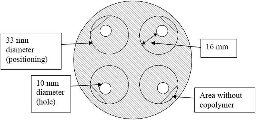 | ||
| Fig. 1 The typical configuration of the prepared thin film sample. | ||
The crystal structures of the samples were examined by Phillips X'Pert Pro XRD with Cu-Kα radiation (1.54056 Å). Step scanned powder XRD data was collected in the 2θ range 10°–80° at room temperature. Detailed structural analysis was performed using SEM (JEOL JSM 6390), Transmission Electron Microscope (JEOL JEM 2100) and FTIR spectroscopy. The piezoelectric property was determined by PFM using SS01 Piezo-d meter, (Sensor Technologie Limited). A conventional ME measurement has been carried out using the lock in amplifier method67 and room temperature dielectric studies were performed using an Agilent 4980 precision LCR meter. The magnetization measurements were performed using Vibrating Sample Magnetometer.
3. Results and discussion
3.1 Structural analysis
Fig. 2(a) shows the crystal structure of different phases of PVDF.93 Among the various crystalline phases of PVDF, α and β phases are predominant. Our interest was on electroactive β phase which can alter the electric behavior. The parallel alignment of dipoles in the β phase create a net surface charge while the net surface charge is zero in α phase as the dipoles cancel out each other due to the random orientation. The phase structure of the film was examined using X-ray diffraction techniques. Fig. 2(b) shows X-ray diffractograms at room temperature of the P(VDF-TrFE)–BiFeO3–NaNbO3 composite films. For the as-cast film a sharp diffraction peak of (200) and (110) planes at 19.9° and 38° (marked by ‘P’) attributed to ferroelectric β phase of P(VDF-TrFE) and are consistent with previously reported results for P(VDF-TrFE) with other molar compositions.13,36,48–51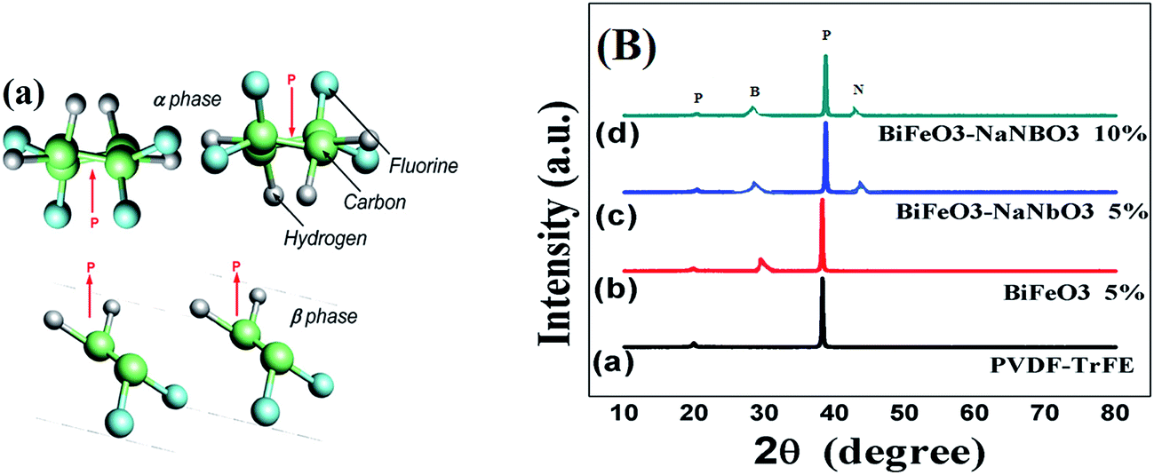 | ||
| Fig. 2 (a) Crystal structure of PVDF different phases, (b) X-ray diffractogram of composite film samples for various nanoparticle concentrations in the polymer matrix. | ||
The other peaks marked by ‘B’ and ‘N’ correspond to BiFeO3 and NaNbO3 phases respectively. The average crystalline size of nanoparticle found from Scherrer equation varies between 100 nm to 150 nm. Fig. 3 shows the SEM images of the as-sintered surfaces of the film. From the SEM images we can observe the nanoparticle aggregates on the polymer matrices. Fig. 4(a) and (b) shows the TEM images of the film samples.
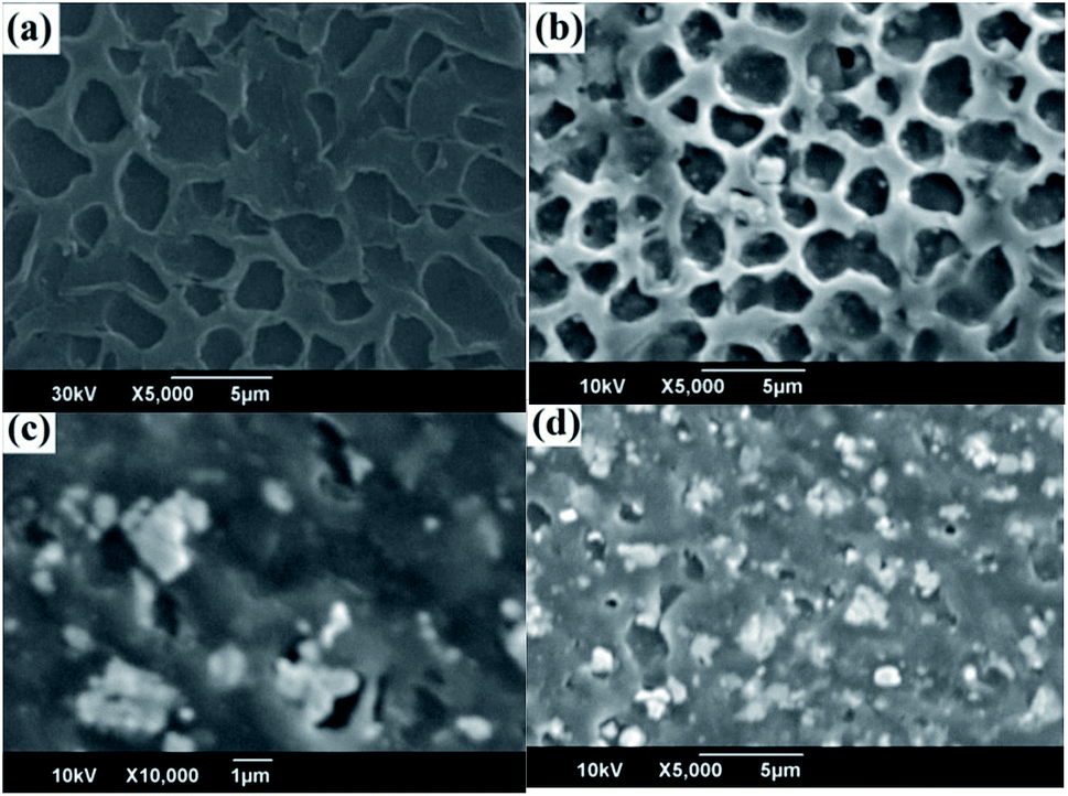 | ||
| Fig. 3 SEM images of BiFeO3–NaNbO3–P(VDF-TrFE) composite film samples for, (a) P(VDF-TrFE) alone, (b) 5% BiFeO3 in the P(VDF-TrFE) matrix, (c) 5% BiFeO3–NaNbO3 in the P(VDF-TrFE) matrix, (d) 10% BiFeO3–NaNbO3 in the P(VDF-TrFE) matrix. | ||
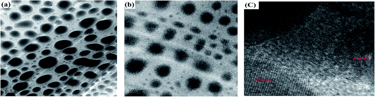 | ||
| Fig. 4 TEM images of BiFeO3–NaNbO3–P(VDF-TrFE) composite film samples for (a) 5% BiFeO3 in the polymer matrix (b) 5% BiFeO3–NaNbO3 in the polymer matrix (c) HRTEM image of 5% BiFeO3–NaNbO3 in the polymer matrix. | ||
Fig. 4(c) shows HRTEM of 5% BiFeO3–NaNbO3 in the polymer matrix which clearly indicates the polycrystalline nature of the film sample. The lattice spacing (d) calculated from the HRTEM image matches with JCPDS values corresponding to BiFeO3 and NaNbO3. The d values of 0.27 nm and 0.31 nm corresponds to (110) and (131) planes of rhombohedral BiFeO3 (JCPDS 74-2016) and orthorhombic NaNbO3 (JCPDS 89-8957) respectively. Fig. 5 shows the AFM images of the film samples. Here, the surface morphology was studied with AFM by taking account of the composite surface. In the 3D AFM picture, we can observe the surface roughness. Fig. 6 shows AFM phase images of samples with 5% and 10% BiFeO3–NaNbO3 in polymer matrix. The force exerted by the AFM tip on the surface will be different for the nano particle and the polymer surface and the phase image may represents the different particles/phases, if present. The force exerted by the AFM tip on the surface will be different for the nano particle and the polymer surface. In the present case a sharp distinction between the polymer and nanoparticles cannot be made as there is no much differences in the phase images.
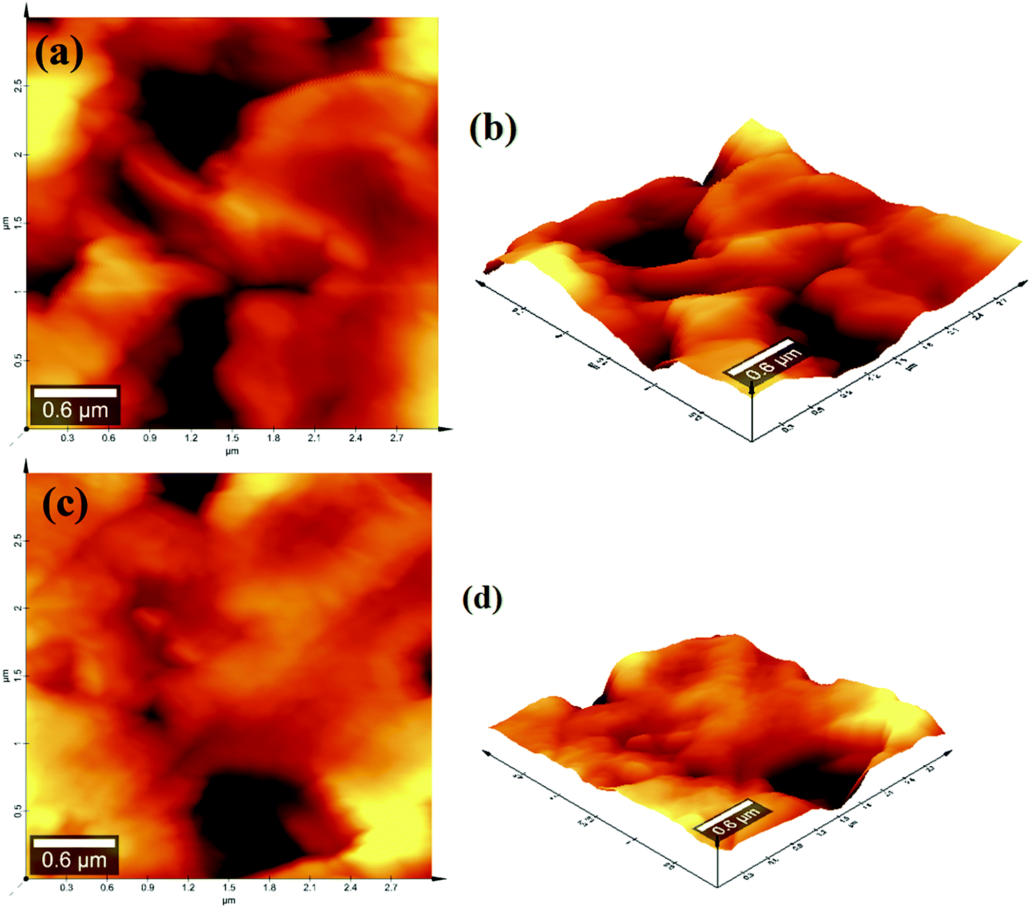 | ||
| Fig. 5 (a) 2D AFM image of 5% BiFeO3–NaNbO3 in the polymer matrix, (b) 3D AFM image of 5% BiFeO3–NaNbO3 in the polymer matrix, (c) 2D AFM image of 10% BiFeO3–NaNbO3 in the polymer matrix, (d) 3D AFM image of 10% BiFeO3–NaNbO3 in the polymer matrix. | ||
 | ||
| Fig. 6 The phase images of the samples (a) 5% BiFeO3–NaNbO3 in polymer matrix, (b) 10% BiFeO3–NaNbO3 in polymer matrix. | ||
Inorder to have more detailed interpretation of the structure of ceramic composite film samples, FTIR spectroscopy is used (Fig. 7). Several vibrational bands for the co-polymer have been assigned to specific confirmations by previous reports.68–71 Characteristic absorption bands due to the electro active β phase at 885 cm−1 (CH2 rocking, CF2 stretching and skeletal C–C stretching) have been found. The band at 1402 cm−1, 1292 cm−1, 1186 cm−1, 885 cm−1, 848 cm−1 are associated with crystalline phase (β) of P(VDF-TrFE) co polymer which shows marginal increase in the absorption intensity irrespective of the nanoparticle addition in the polymer film. From the report of Kim et al.,71 it was observed that the changes in the intensity at 1292 cm−1 bands is highly dependent on the amount of ferroelectric phase content and can be suitable candidate for monitoring the ferroelectric crystalline phase.71 The bands at 3439 cm−1, 2928 cm−1, 2335 cm−1 and 1385 cm−1 are due to the ceramic nano particle. The broad absorption band in the range of 3439 cm−1 is assigned to O–H stretching and the 2928 cm−1 band is due to C–H stretching vibrations. A peak at 2335 cm−1 was representative of nitrile72 and the band located at 1385 cm−1 indicate the existence of nitrate ions.67,73,74
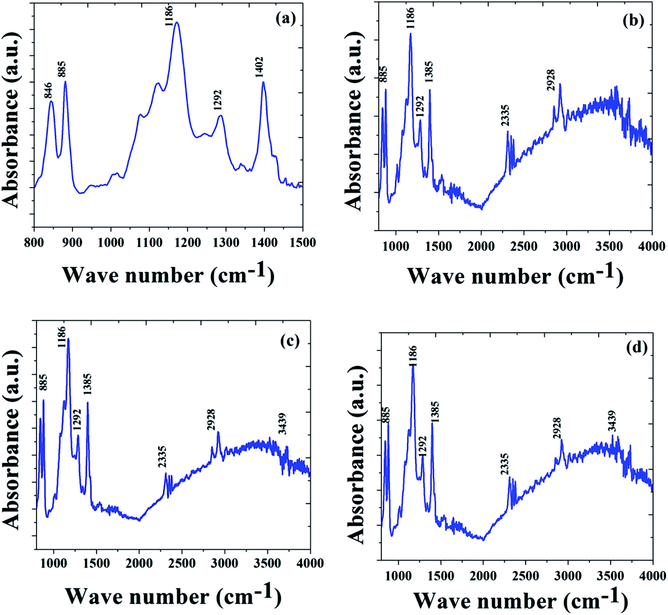 | ||
| Fig. 7 FTIR spectra of (BiFeO3–NaNbO3)–P(VDF-TrFE) composite film samples for (a) P(VDF-TrFE) alone, (b) 5% BiFeO3 in the P(VDF-TrFE) matrix, (c) 5% BiFeO3–NaNbO3 in the P(VDF-TrFE) matrix, (d) 10% BiFeO3–NaNbO3 in the P(VDF-TrFE) matrix. | ||
The Raman spectra and corresponding Raman images of the samples are shown in Fig. 8. The intensity of the peak from PVDF absorbance (1430 cm−1) remains unaltered in all the spectra. Raman spectra also confirm the presence of β phase crystal domains of P(VDF-TrFE) through out the films. By group theory, there are 13 active Raman modes present in BFO for rhombohedral R3c structure. In our samples characteristic modes at 132 cm−1, 169 cm−1, 221 cm−1, 254 cm−1 are dominated by the Bi–O covalent bonds and these four characteristic modes results the origin of ferroelectric order in the composite. The other modes which lie between 300 cm−1 to 600 cm−1 are characteristic modes of BiFeO3.75 Because of local stress and a large number of point defects, several fundamental modes are not detected in the spectrum. The Raman modes in the low wavenumber region 150–300 cm−1 are characteristic of the bending modes of Nb–O–Nb, whereas the band at 992 cm−1 is due to a small concentration of the Nb![[double bond, length as m-dash]](https://www.rsc.org/images/entities/char_e001.gif) O surfaces.76–78 The Raman band in the range of 500–700 cm−1 (612 cm−1) and 150–300 cm−1 (251 cm−1) are assigned to the Nb–O–Nb vibrations of the NbO6 octahedrons present in the crystalline structure of NaNbO3. Moreover, the peak at about 871 cm−1 is related to the Nb–O vibrations of isolated octahedras.79
O surfaces.76–78 The Raman band in the range of 500–700 cm−1 (612 cm−1) and 150–300 cm−1 (251 cm−1) are assigned to the Nb–O–Nb vibrations of the NbO6 octahedrons present in the crystalline structure of NaNbO3. Moreover, the peak at about 871 cm−1 is related to the Nb–O vibrations of isolated octahedras.79
 | ||
| Fig. 8 Confocal Raman spectra of BiFeO3–NaNbO3–P(VDF-TrFE) composite film samples for (a) P(VDF-TrFE) alone, (b) 5% BiFeO3 in the P(VDF-TrFE) matrix, (c) 5% BiFeO3–NaNbO3 in the P(VDF-TrFE) matrix, (d) 10% BiFeO3–NaNbO3 in the P(VDF-TrFE) matrix. | ||
The inset shows corresponding confocal Raman images. The conventional Raman imaging method using a narrow spectral range corresponding to a characteristic Raman band of each chemical species is adopted. The contrast and resolution of Raman images can be greatly increased by positioning a sharp silver tip near the laser focus. The simultaneously recorded topographic 3D image is presented in the inset of each spectrum. The bright field region of the Raman image represents the nanoparticles and dark region represents the P(VDF-TrFE) matrix.
3.2 Piezoelectric and magnetoelectric studies
Fig. 9 shows the topographic and PFM images of 5% BiFeO3–NaNbO3 and 10% BiFeO3–NaNbO3 in PVDF-TrFE matrix. The topographic image reveals a morphologic structure consisting of grains in the nanometer size. In the vertical PFM amplitude images shown in Fig. 9(c) and (d), inhomogeneously distributed regions with opposite contrast are present. White and dark regions in the PFM images correspond to domains with the polarization vector oriented towards the surface of the sample and to the bottom electrode respectively.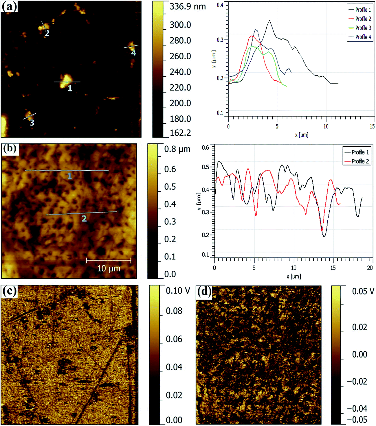 | ||
| Fig. 9 (a) Surface topography of 5% BiFeO3–NaNbO3 in the polymer matrix (b) surface topography of 10% BiFeO3–NaNbO3 in the polymer matrix (c) PFM image of 5% BiFeO3–NaNbO3 in the polymer matrix (d) PFM image of 10% BiFeO3–NaNbO3 in the polymer matrix. | ||
These images are reminiscent of the typical PFM contrast observed in polycrystalline ferroelectric ceramics.80,81 Domain walls appear as narrow dark lines with a characteristically weak amplitude signal and a smallest measured width. The high value of the PFM amplitude signal suggests that the molecular chains in these crystallites are aligned parallel to the substrate. The d33 values were determined from the PFM images and it is found to be 34 pC/N and 38 pC/N for 5% BiFeO3–NaNbO3 in P(VDF-TrFE) and 10% BiFeO3–NaNbO3 in P(VDF-TrFE) respectively. This is the most important evidence that the present material is good piezoelectric. It can be seen that the vertical piezoelectric coefficient d33 increases by increasing the % vol of nanoparticle in the polymer.
The piezoelectric coefficient d33 is also measured using the direct method often called Berlincourt method (SS01 Piezo-d meter, Sensor Technologie Limited)82 by applying a force of 2 N and the values are tabulated in Table 2. There is a slight difference in the d33 values measured by PFM technique and Berlincourt method. However, from the two techniques employed it could be clarified that the material is piezoelectric in nature. The difference in the measured values could be attributed to the fact that in the PFM technique, the measurements have been done on the entire film sample by keeping the entire film on the sample holder and the images were taken from different regions. But in Berlincourt method, only a small portion of the sample has been peeled out and the measurements were carried out in this portion.
| Sl. no. | Concentration (wt%) of ceramic particle | d33 values (pC/N) |
|---|---|---|
| 1 | 0% | 19±2 |
| 2 | 5% BiFeO3 | 23±2 |
| 3 | 5% BiFeO3–NaNbO3 | 22±2 |
| 4 | 10% BiFeO3–NaNbO3 | 21±2 |
In layered multiferroics, the in plane stresses arouse multiferroism.28–36 Among the various possibilities, interfacial strain coupling between the ferroelectric and magnetic phases via the piezoelectric effect is the most investigated route for the enhancement of multiferroic property in layered structures. Hence the piezoelectric property and magnetoelectric property are very much related. The piezoelectric charge coefficient d33 is one of the fundamental parameters defining the piezoelectric activity of a material, basically the higher the d33 value the more active the material is. The d33 coefficient is defined as the charge produced for an applied stress or the strain for an applied voltage and these are theoretically equivalent.83
The coexistence of electric and magnetic phases in the samples which brings about the magnetoelectric (ME) coupling was measured using a Lock-in amplifier. The A.C. magnetic field dependence of ME voltage at room temperature is shown in Fig. 10. The magnetoelectric response for three different fixed DC field is measured. For every composition, it shows linear dependence on the applied field. The value of magnetoelectric coupling coefficient (α) is determined from the slope of the ME curve. The values of magnetoelectric coupling coefficient (α) are tabulated in Table 3. ME response of ceramic-polymer thin film shows very good result compared to the BiFeO3–NaNbO3 ceramic nano powder which we found in our previous experiments.40 Here we can say that the piezoelectric polymer P(VDF-TrFE) enhances the ME response of the film samples.36,84
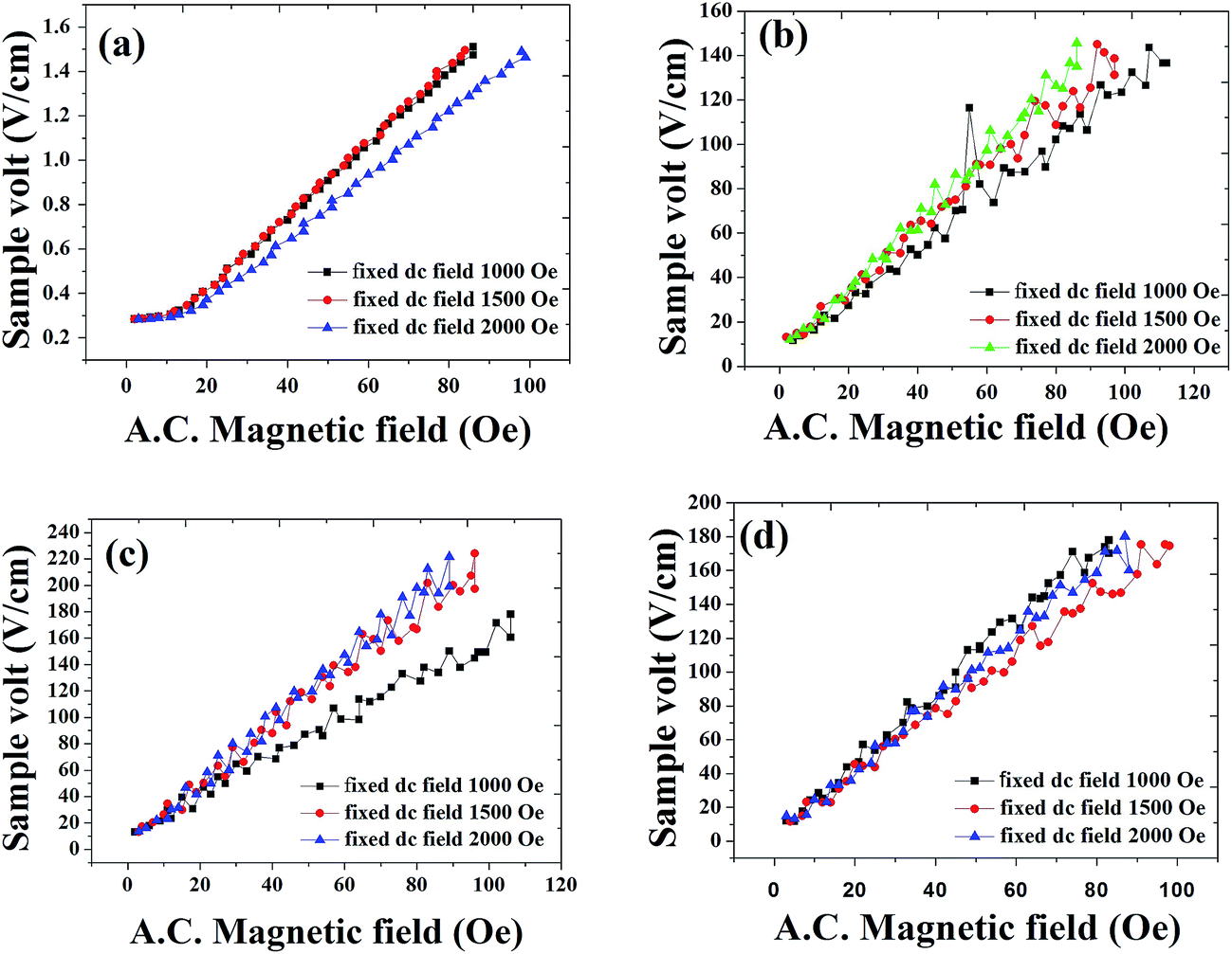 | ||
| Fig. 10 ME voltage as a function of AC magnetic field at different fixed DC field for BiFeO3–NaNbO3–P(VDF-TrFE) composite film samples for (a) P(VDF-TrFE) alone, (b) 5% BiFeO3 in the P(VDF-TrFE) matrix, (c) 5% BiFeO3–NaNbO3 in the P(VDF-TrFE) matrix, (d) 10% BiFeO3–NaNbO3 in the P(VDF-TrFE) matrix. | ||
| Sl. no. | Sample name | ME coefficient (α) (V cm−1 Oe−1) | |
|---|---|---|---|
| For fix dc 1000 Oe | For fix dc 2000 Oe | ||
| 1 | P(VDF-TrFE) | 0.01 | 0.02 |
| 2 | 5% BiFeO3 | 1.26 | 1.88 |
| 3 | 5% BiFeO3–NaNbO3 | 1.48 | 2.42 |
| 4 | 10% BiFeO3–NaNbO3 | 1.99 | 2.42 |
For increasing vol% of ceramic nanoparticles, the ME response is found to be increasing in the composite. Increase in the ME voltage according to the percentage increase of nanoparticles is explained by the increase in the magnetostriction due to the substantial increase of the magnetostrictive phase (i.e. BiFeO3). For higher concentrations of nanoparticle in the polymer matrix, magnetoelectric coupling coefficient of 2.4 V cm−1 Oe−1 is obtained. Even if BFO thin films show good magnetoelectric coupling at room temperature,85 they often show high leakage currents due to oxygen vacancies and mixed Fe valences.86,87 However, multilayer heterostructures of BiFeO3 show high magnetoelectric (ME) coefficients. BiFeO3–BaTiO3 composite film have a ME coefficient up to 24 V cm−1 Oe−1 at 300 K88 which is much higher than that of a single-phase BiFeO3 reference film (4.2 V cm−1 Oe−1).86 Fig. 11 shows the ME voltage variations of the film samples with DC magnetic field.
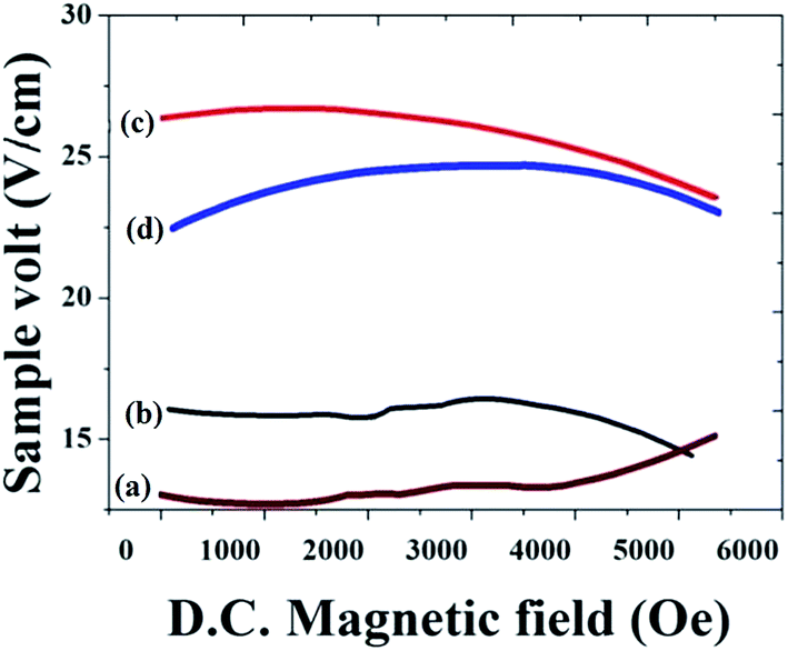 | ||
| Fig. 11 ME voltage as a function of DC magnetic field for BiFeO3–NaNbO3–P(VDF-TrFE) composite film samples for (a) P(VDF-TrFE) alone, (b) 5% BiFeO3 in the P(VDF-TrFE) matrix, (c) 5% BiFeO3–NaNbO3 in the P(VDF-TrFE) matrix, (d) 10% BiFeO3–NaNbO3 in the P(VDF-TrFE) matrix. | ||
3.3 Magnetic study
Magnetic hysteresis loop of 5% BiFeO3–NaNbO3 and 10% BiFeO3–NaNbO3 in PVDF-TrFE matrix at room temperature is shown in Fig. 12(a). A good hysteresis behaviour which is saturated within the field of 30 kOe can be observed indicating a ferromagnetic nature at room temperature. The ferromagnetism of these samples could be a result of the reduction of particle size. The weak ferromagnetism observed in BFO nanoparticles is due to the nonexact compensation of the spins with a decrease in particle size.97 When the particle size decreases, number of surface asymmetry atoms increases. Due to this, the angle of the helical ordered spin arrangement is changed and a net magnetic moment appears.99,101–105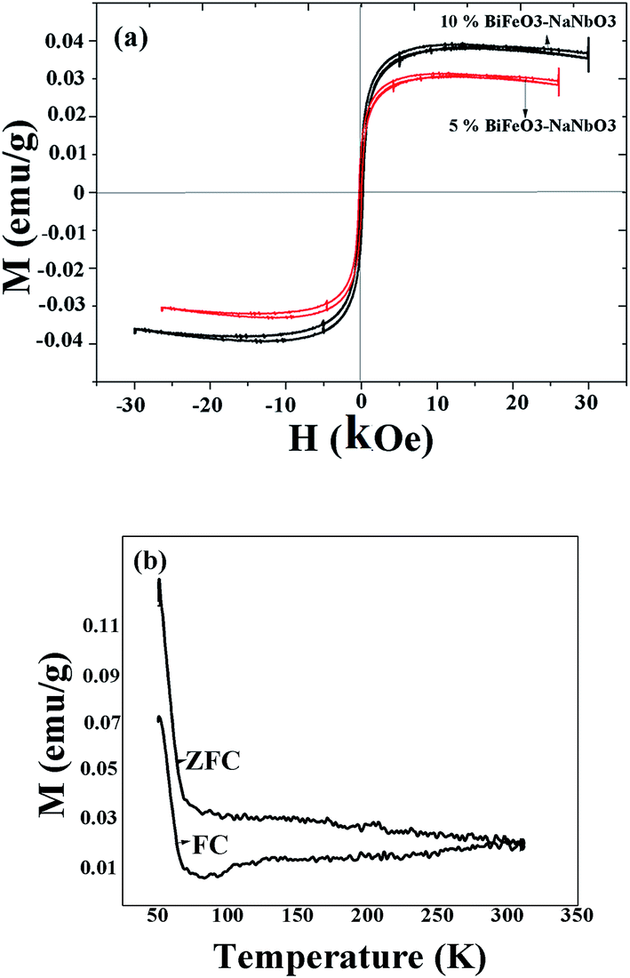 | ||
| Fig. 12 (a) Hysteresis loop of the 5% BiFeO3–NaNbO3 and 10% BiFeO3–NaNbO3 in PVDF-TrFE matrix, (b) temperature dependent magnetization study of 10% BiFeO3–NaNbO3 in PVDF-TrFE matrix. | ||
The main possibility is the high piezoelectricity due to the presence of P(VDF-TrFE) co-polymer and the other is due to the NaNbO3 content which also has good electromechanical property.37 Since the XRD patterns have not detected any impurity phase, the properties which have been observed could be due to the contribution of the ceramic part and co-polymer itself. The maximum magnetization attained is different for two compositions and found to be 0.04 emu g−1 for 10% BiFeO3–NaNbO3 and 0.03 emu g−1 for 5% of BiFeO3–NaNbO3 in P(VDF-TrFE) matrix. The magnetization value is found to be increasing with increase in the amount of nanoparticle in the polymer matrix. While the coercivity (Hc) and remanant magnetization (Mr) are almost same for the two compositions. The coercive field (Hc) is almost 0.9 kOe for both compositions. The ZFC and FC curves of 10% BiFeO3–NaNbO3 powder in the PVDF-TrFE matrix measured under a magnetic field of 200 Oe is shown in Fig. 12(b). The divagation of ZFC and FC magnetizations close to room temperature shows the room temperature multiferroic property of the sample and also the spin glass behaviour.100 These results are consistent with the phenomenon observed in BiFeO3 nanoparticles.89,90 In the case of non magnetic materials there will not be any difference in the FC and ZFC curve.17,100 Some reports indicate that the splitting of FC–ZFC curve is due to the coexistence of antiferromagnetic and ferromagnetic phases which is usually observed in core shell type BiFeO3 nanoparticles.98 The FC and ZFC magnetizations increases gradually with decreasing temperature, and it shows an anomalous behaviour below 100 K which may be due to the superparamagnetic behaviour commonly observed in BFO.89,90 The study lead by T. J. Park et al. reports a size reduction from bulk to nano change the paramagnetic substance to ferromagnetic.89
3.4 Electric study
The frequency dependence of real part of dielectric permittivity (ε) and dielectric loss (tanδ) of BiFeO3–NaNbO3 ceramics at room temperature is plotted in Fig. 13 which follows inverse dependence on frequency, normally followed by almost all ferroelectric materials. Compared to the dielectric properties of BiFeO3, the present composite film samples possess larger ε whereas the dielectric loss is obviously reduced.91,92
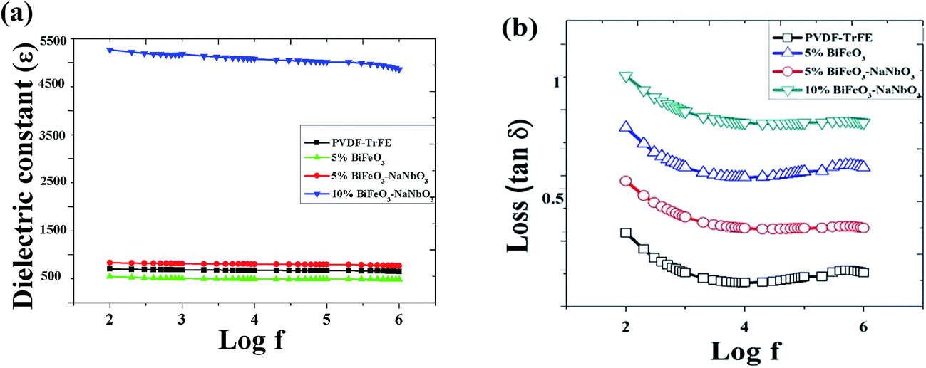 | ||
| Fig. 13 Dielectric relaxation (a) the real part (b) the imaginary part of dielectric dispersion of BiFeO3–NaNbO3–P(VDF-TrFE) composite film samples. | ||
The dielectric constant of the ceramic polymer composite is very high for the BiFeO3–NaNbO3 volume fraction of 10 vol%, which is the highest dielectric constant reported so far for the polymer composite materials. A nearly good value of dielectric constant for polymer ceramic composite is observed in BaTiO3–PVDF composite.93,95 The ultra-high dielectric constant can be caused by conductive behavior or electric heterogeneous nature of the composites or interfacial polarization among ceramic-polymer interfaces. In the electrical property of polycrystalline samples, the grain boundary region plays an important role. The inhomogeneity between the grain and grain boundary regions and reduction of movable charges is one of the reasons for ultrahigh value of dielectric constant.94
The dielectric constant of the ceramic polymer composite is more than 5000 for the BiFeO3–NaNbO3 volume fraction of 10 vol%, which is the highest dielectric constant reported so far for the polymer composite materials. The dielectric constant of the film for BiFeO3 alone in the polymer matrix is less than pure P(VDF-TrFE) as BiFeO3 has a low dielectric compared to P(VDF-TrFE) and NaNbO3. The dielectric constant of the composite increases with increasing vol% of BiFeO3–NaNbO3 ceramics which indicate the dielectric property can be tuned by changing the NaNbO3 content. The decaying trend of dielectric loss with frequency can be ascribed to reduced ohmic and polarization losses. As a matter of fact, frequency increase is equivalent to reduced available times for free electrons to travel throughout the conductive network in each half cycle of alternating field, i.e. reduced ohmic loss. Furthermore, due to interfacial polarization relaxation, the interfacial charge polarization decays with frequency leading to low dipole moment and polarization loss.
Ferroelectric polarization–electric field (PE) loops of 5% BiFeO3–NaNbO3 in P(VDF-TrFE) and pure P(VDF-TrFE) are shown in Fig. 14. The polarization value of pure P(VDF-TrFE) is higher than that of ceramic-polymer composite. It means that the electric polymer P(VDF-TrFE) contribute mainly to the electric property of our samples. Pure co-polymer shows PE loop with a coercive field (Ec) of 2 kV cm−1 and saturation polarization of 10.9 μC cm−2 which is consistent with the previous reports of P(VDF-TrFE).96 The ceramic-polymer composite have saturation polarization of 8 μC cm−2 which is mainly due to the ferroelectric phase of co-polymer and NaNbO3. Probably the smaller volume fraction of the polymer phase may be the reason for reduction of polarization value in the ceramic-polymer composite compared to PVDF-TrFE alone. Both the remanant polarization and coercive field are high for P(VDF-TrFE) than the ceramic-polymer composite.
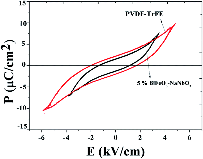 | ||
| Fig. 14 Ferroelectric hysteresis loop of PVDF-TrFE and 5% BiFeO3–NaNbO3 in P(VDF-TrFE) matrix. | ||
4. Conclusion
Our findings lead to a novel way for preparing energy storing and transforming materials with ultrahigh dielectric constant and room temperature magnetoelectric coupling which are required in embedded capacitors, microelectromechanical systems, ultrasonic resonators, high power transducers, actuators etc. A series of BiFeO3–NaNbO3–P(VDF-TrFE) composite films with various volume fraction of BiFeO3–NaNbO3 in the polymer matrix were prepared by using spin coating technique. The nanocomposite containing 10 vol% of BiFeO3–NaNbO3 ceramics in the polymer have an ultrahigh dielectric constant at 1 kHz frequency which is very much higher than pure P(VDF-TrFE) and pure BFO. The high d33 value observed is a remarkable improvement which alter the magnetic and electric properties of the composite. The room temperature ferromagnetism and magnetoelectric coupling promise tailored applications of current material in various fields. In summary, the giant enhancement in dielectric property as well as magnetoelectric coupling in the film sample make them essential for visualizing the real application of multiferroics. Hence in the design of advanced multiferroic materials, multiphase BiFeO3–NaNbO3–P(VDF-TrFE) composite film is an attractive and successful approach to overcome the limitations of intrinsic single phase multiferroics.Acknowledgements
The authors would like to acknowledge the financial support from DST – Govt. of India through the Nano Mission, PURSE, FIST Programs, and UGC – Govt. of India for the SAP program. We also express our gratitude to Mr Sreenivas, APE Research Italy for the PFM measurements. One of the authors RPU would like to acknowledge UGC-Govt. of India for the RFSMS fellowship.References
- W. Qin, B. Xu and S. Ren, Nanoscale, 2015, 7, 9122–9132 RSC.
- G. Caruntu, A. Yourdkhani, M. Vopsaroiu and G. Srinivasan, Nanoscale, 2012, 4, 3218–3227 RSC.
- S. Sun, Y. Huang, G. Wang, J. Wang, Z. Fu, R. Peng, R. J. Knize and Y. Lu, Nanoscale, 2014, 6, 13494–13500 RSC.
- H. Miao, X. Zhou, S. Dong, H. Luo and F. Li, Nanoscale, 2014, 6, 8515–8520 RSC.
- H. Trivedi, V. V. Shvartsman, D. C. Lupascu, M. S. A. Medeiros, R. C. Pullar, A. L. Kholkin, P. Zelenovskiy, A. Sosnovskikh and V. Y. Shur, Nanoscale, 2015, 7, 4489–4496 RSC.
- B. Y. Wang, H. T. Wang, S. B. Singh, Y. C. Shao, Y. F. Wang, C. H. Chuang, P. H. Yeh, J. W. Chiou, C. W. Pao, H. M. Tsai, H. J. Lin, J. F. Lee, C. Y. Tsai, W. F. Hsieh, M. H. Tsaif and W. F. Pong, RSC Adv., 2013, 3, 7884 RSC.
- B. Raneesh, A. Saha, D. Das, P. Sreekanth, R. Philip and N. Kalarikkal, RSC Adv., 2015, 5, 12480 RSC.
- J. Allibe, S. Fusil, K. Bouzehouane, C. Daumont, D. Sando, E. Jacquet, C. Deranlot, M. Bibes and A. Barthe, Nano Lett., 2012, 12, 1141–1145 CrossRef CAS PubMed.
- M. Stingaciu, P. G. Reuvekamp, C. W. Tai, R. K. Kremer and M. Johnson, J. Mater. Chem. C, 2014, 2, 325 RSC.
- C. Binek, Physics, 2013, 6, 13 CrossRef.
- G. Lawes and G. Srinivasan, J. Phys. D: Appl. Phys., 2011, 44, 243001 CrossRef.
- V. V. Lazenka, G. Zhang, J. Vanacken, I. Makoed, A. F. Ravinski and V. V. Moshchalkov, J. Phys. D: Appl. Phys., 2012, 45, 125002 CrossRef.
- J. Ma, J. Hu, Z. Li and C. W. Nan, Adv. Mater., 2011, 23, 1062 CrossRef CAS PubMed.
- C. A. F. Vaz, J. Hoffman, C. H. Ahn and R. Ramesh, Adv. Mater., 2010, 22, 2900 CrossRef CAS PubMed.
- P. Martins and S. Lanceros Méndez, Adv. Funct. Mater., 2013, 23, 3371 CrossRef CAS.
- N. Lei, S. Park, P. Lecoeur, D. Ravelosona and C. Chappert, Phys. Rev. B: Condens. Matter Mater. Phys., 2011, 84, 012404 CrossRef.
- O. D. Jayakumar, B. P. Mandal, J. Majeed, G. Lawes, R. Naik and A. K. Tyagi, J. Mater. Chem. C, 2013, 1, 3710 RSC.
- M. Li, Y. Wang, Y. Shen, J. Gao, J. Li and D. Viehland, J. Appl. Phys., 2013, 114, 144501 CrossRef.
- Y. Chen, J. Wang, M. Liu, J. Lou, N. X. Sun, C. Vittoria and V. G. Harris, Appl. Phys. Lett., 2008, 93, 112502 CrossRef.
- Z. Zhou, T. X. Nan, Y. Gao, X. Yang, S. Beguhn, M. Li, Y. Lu, J. L. Wang, M. Liu, K. Mahalingam, B. M. Howe, G. J. Brown and N. X. Sun, Appl. Phys. Lett., 2013, 103, 232906 CrossRef.
- R. Jahns, A. Piorra, E. Lage, C. Kirchhof, D. Meyners, J. L. Gugat, M. Krantz, M. Gerken, R. Knochel and E. Quandt, J. Am. Ceram. Soc., 2013, 96, 1673–1681 CrossRef CAS.
- H. Zhao, X. Peng, L. Zhang, J. Chen, W. Yan and X. Xing, Appl. Phys. Lett., 2013, 103, 082904 CrossRef.
- N. Jedrecy, H. J. von Bardeleben, V. Badjeck, D. Demaille, D. Stanescu, H. Magnan and A. Barbier, Phys. Rev. B: Condens. Matter Mater. Phys., 2013, 88, 121409 CrossRef.
- W. Liang, Z. Li, Z. Bi, T. Nan, H. Du, C. Nan, C. Chen, Q. Jia and Y. Lin, J. Mater. Chem. C, 2014, 2, 708–714 RSC.
- S. Mukherjee, A. Roy, S. Auluck, R. Prasad, R. Gupta and A. Garg, Phys. Rev. Lett., 2013, 111, 087601 CrossRef PubMed.
- J. Zhai, Z. Xing, S. Dong, J. Li and D. Viehland, J. Am. Ceram. Soc., 2008, 91, 351–358 CrossRef CAS.
- Y. Lin, N. Cai, J. Zhai, G. Liu and C. W. Nan, Phys. Rev. B: Condens. Matter Mater. Phys., 2005, 72, 012405 CrossRef.
- N. Lei, S. Park, P. Lecoeur, D. Ravelosona and C. Chappert, Phys. Rev. B: Condens. Matter Mater. Phys., 2011, 84, 012404 CrossRef.
- M. Liu, O. Obi, Z. Cai, J. Lou, G. Yang, K. S. Ziemer and N. X. Sun, J. Appl. Phys., 2010, 107, 073916 CrossRef.
- J. Lou, M. Liu, D. Reed, Y. Ren and N. X. Sun, Adv. Mater., 2009, 21, 4711 CrossRef CAS.
- Z. Wang, R. Viswan, B. Hu, J. F. Li, V. G. Harris and D. Viehland, J. Appl. Phys., 2012, 111, 034108 CrossRef.
- Z. Li, J. Hu, L. Shu, Y. Gao, Y. Shen, Y. Lin and C. W. Nan, J. Appl. Phys., 2012, 111, 033918 CrossRef.
- C. Pettiford, J. Lou, L. Russell and N. X. Sun, Appl. Phys. Lett., 2008, 92, 122506 CrossRef.
- F. Zighem, D. Faurie, S. Mercone, M. Belmeguenai and H. Haddadi, J. Appl. Phys., 2013, 114, 073902 CrossRef.
- M. Weiler, A. Brandlmaier, S. Gepreags, M. Althammer, M. Opel, C. Bihler, H. Huebl, M. S. Brandt, R. Gross and S. T. B. Goennenwein, New J. Phys., 2009, 11, 013021 CrossRef.
- A. Brandlmaier, S. Gepreags, G. Woltersdorf, R. Gross and S. T. B. Goennenwein, J. Appl. Phys., 2011, 110, 043913 CrossRef.
- C. W. Nan, Phys. Rev. B: Condens. Matter Mater. Phys., 1994, 50, 6082–6088 CrossRef CAS.
- C. H. Sim, A. Pan and J. Wang, J. Appl. Phys., 2008, 103, 124109 CrossRef.
- D. Mazumdar, V. Shelke, M. Iliev, S. Jesse, A. Kumar, S. V. Kalinin, A. P. Baddorf and A. Gupta, Nano Lett., 2010, 10, 2555–2561 CrossRef CAS PubMed.
- R. P. Ummer, P. Sreekanth, B. Raneesh, R. Philip, D. Rouxel, S. Thomas and N. Kalarikkal, RSC Adv., 2015, 5, 67157 RSC.
- L. Mitoseriu, et al., J. Eur. Ceram. Soc., 2007, 27, 4379–4382 CrossRef CAS.
- S. Tan, X. Hu, S. Ding, Z. Zhang, H. Li and L. Yang, J. Mater. Chem. A, 2013, 1, 10353 CAS.
- Y. Feng, W. L. Li, Y. F. Hou, Y. Yu, W. P. Cao, T. D. Zhanga and W. D. Fei, J. Mater. Chem. C, 2015, 3, 1250 RSC.
- L. E. Cross, Jpn. J. Appl. Phys., 1995, 5, 34 Search PubMed.
- M. V. Gandhi and B. S. Thomson, Smart materials and structures, Chapman and Hall Publishing group, London, 1992, vol. 5, p. 310 Search PubMed.
- Y. C. Zhou, Y. Y. Bai, K. Yu, Y. Kang and H. Wang, Appl. Phys. Lett., 2013, 102, 252903–252905 CrossRef.
- T. Zhou, J. W. Zha, R. Y. Cui, B. H. Fan, J. K. Yuan and Z. M. Dang, ACS Appl. Mater. Interfaces, 2011, 3, 2184–2188 CAS.
- W. M. Xia, Z. Xu, F. Wen and Z. C. Zhang, Ceram. Int., 2012, 38, 1071–1075 CrossRef CAS.
- V. S. Nguyen, L. Badie, E. Senechault, E. Blampain, B. Vincent and C. Venet, et al., IEEE Trans. Sonics Ultrason., 2013, 60, 2039–2043 CrossRef PubMed.
- S. G. Lu, J. Z. Jin, X. Zhou, Z. Fang and Q. Wang, J. Appl. Phys., 2011, 110, 10–11 Search PubMed.
- X. Liu, S. Liu, M. G. Han, L. Zhao, H. Deng, J. Li and Y. Zhu, Nanoscale Res. Lett., 2013, 8, 37 CrossRef PubMed.
- N. Jedrecy, H. J. von Bardeleben, V. Badjeck, D. Demaille, D. Stanescu, H. Magnan and A. Barbier, Phys. Rev. B: Condens. Matter Mater. Phys., 2013, 88, 121409 CrossRef.
- W. Liang, Z. Li, Z. Bi, T. Nan, H. Du, C. Nan, C. Chen, Q. Jia and Y. Lin, J. Mater. Chem. C, 2014, 2, 708–714 RSC.
- S. Mukherjee, A. Roy, S. Auluck, R. Prasad, R. Gupta and A. Garg, Phys. Rev. Lett., 2013, 111, 087601 CrossRef PubMed.
- J. Y. Zhai, Z. Xing, S. Dong, J. Li and D. Viehland, J. Am. Ceram. Soc., 2008, 91, 351–358 CrossRef CAS.
- Y. Lin, N. Cai, J. Zhai, G. Liu and C. W. Nan, Phys. Rev. B: Condens. Matter Mater. Phys., 2005, 72, 012405 CrossRef.
- B. Chu, X. Zhou, K. Ren, B. Neese, M. Lin, Q. Wang, F. Bauer and Q. M. Zhang, Science, 2006, 313, 334 CrossRef CAS PubMed.
- Z. M. Dang, Y. H. lin and C. W. Nan, Adv. Mater., 2003, 15, 1625 CrossRef CAS.
- Q. Gao, J. I. Scheinbeim and B. A. Newman, J. Polym. Sci., Part B: Polym. Phys., 1999, 37, 3217–3225 CrossRef CAS.
- V. S. Nguyen, L. Badie, E. Senechault, E. Blampain, B. Vincent and C. Venet, et al., IEEE Trans. Sonics Ultrason., 2013, 60, 2039–2043 CrossRef PubMed.
- V. S. Nguyen, L. Badie, E. Lamouroux, B. Vincent, F. D. Dos Santos and M. Aufray, et al., J. Appl. Polym. Sci., 2013, 129, 391–396 CrossRef CAS.
- V. S. Nguyen, D. Rouxel, B. Vincent, L. Badie, F. D. Dos Santos and E. Lamouroux, et al., Appl. Surf. Sci., 2013, 279, 204–211 CrossRef CAS.
- V. S. Nguyen, D. Rouxel, M. Meier, B. Vincent, A. Dahoun and S. Thomas, et al., Polym. Eng. Sci., 2014, 54, 1280–1288 CAS.
- W. M. Xia, Z. Xu, F. Wen and Z. C. Zhang, Ceram. Int., 2012, 38, 1071–1075 CrossRef CAS.
- Q. M. Zhang, H. Li, M. Poh, F. Xia, Z. Y. Cheng, H. Xu and C. Huang, Nature, 2002, 419, 284 CrossRef CAS PubMed.
- S. X. Huo, S. L. Yuan, Y. Qiu, Z. Z. Ma and C. H. Wang, Mater. Lett., 2012, 68, 8–10 CrossRef CAS.
- J. Xu, H. Ke and D. Jia, J. Alloys Compd., 2009, 472, 473 CrossRef CAS.
- K. Tashiro and M. Kobayashi, Spectrochim. Acta, Part A, 1994, 50, 1573 CrossRef.
- K. J. Kim, N. M. Reynolds and S. L. Hsu, Macromolecules, 1989, 22, 4395 CrossRef.
- N. M. Reynolds, K. J. Kim, C. Chang and S. L. Hsu, Macromolecules, 1989, 22, 1092 CrossRef CAS.
- K. J. Kim, N. M. Reynolds and S. L. Hsu, J. Polym. Sci., Part B: Polym. Phys., 1993, 31, 1555 CrossRef CAS.
- M. H. Nguyen, S. Lee and W. M. Kriven, J. Mater. Res., 1999, 14, 3417–3426 CrossRef CAS.
- S. Ghosh, S. Dasgupta, A. Sen and H. S. Maiti, J. Am. Ceram. Soc., 2005, 88, 1349–1352 CrossRef CAS.
- H. Zhang, X. Fu, S. Niu and Q. Xin, J. Alloys Compd., 2008, 457, 61–65 CrossRef CAS.
- S. K. Pradhan, J. Mater. Sci.: Mater. Electron., 2013, 24, 3581–3586 CrossRef CAS.
- E. Heracleous and A. A. Lemonidou, J. Catal., 2006, 237, 162–174 CrossRef CAS.
- J. M. Jehng and I. E. Wachs, Chem. Mater., 1991, 3, 100–107 CrossRef CAS.
- B. X. Huang, K. Wang, J. S. Church and Y. S. Li, Electrochim. Acta, 1999, 44, 2571–2577 CrossRef CAS.
- P. F. Graca, M. G. Ferreirada Silva and M. A. Valente, Solid State Sci., 2009, 11, 570–577 CrossRef.
- I. Coondoo, N. Panwar, I. Bdikin, V. S. Puli, R. S. Katiyar and A. L. Kholkin, J. Phys. D: Appl. Phys., 2012, 45, 055302 CrossRef.
- A. Kholkin, I. Bdikin, T. Ostapchuk and J. Petzelt, Appl. Phys. Lett., 2008, 93, 222905 CrossRef.
- D. Berlincourt and H. Krueger, J. Appl. Phys., 1959, 30, 1804–1810 CrossRef CAS.
- D. Damjanovic and M. Demartin, J. Phys.: Condens. Matter, 1997, 9, 4943 CrossRef CAS.
- X. Liu, S. Liu, M. G. Han, L. Zhao, H. Deng, J. Li and Y. Zhu, Nanoscale Res. Lett., 2013, 8, 37 CrossRef PubMed.
- P. Rovillain, R. de Susa, Y. Gallais, A. Sacuto, M. A. Measson, D. Colson, A. Forget, M. Bibes, A. Barthélémy and M. Cazayous, Nat. Mater., 2010, 9, 975 CrossRef CAS PubMed.
- G. W. Pabst, L. W. Martin, Y. H. Chu and R. Ramesh, Appl. Phys. Lett., 2007, 90, 072902 CrossRef.
- F. Bern, P. Schwinkendorf, A. Setzer, M. Lorenz, M. Grundmann, I. Vrejoiu and M. Ziese, J. Phys.: Condens. Matter, 2014, 47, 135303 Search PubMed.
- M. Lorenz, G. Wagner, V. Lazenka, P. Schwinkendorf, H. Modarresi, M. J. Van Bael, A. Vantomme, K. Temst, O. Oeckler and M. Grundmann, Appl. Phys. Lett., 2015, 106, 012905 CrossRef.
- T. J. Park, G. C. Papaefthymiou, A. J. Viescas, A. R. Moodenbaugh and S. S. Wong, Nano Lett., 2007, 7, 766–772 CrossRef CAS PubMed.
- B. Liu, B. Hu and Z. Du, Chem. Commun., 2011, 47, 8166–8168 RSC.
- M. M. Kumar, V. R. Palkar, K. Srinivas and S. V. Suryanarayana, Appl. Phys. Lett., 2000, 76, 2764 CrossRef CAS.
- A. K. Pradhan, K. Zhang, D. Hunter, J. B. Dadson, G. B. Loutts, P. Bhattacharya, R. Katiyar, J. Zhang, D. J. Sellmyer, U. N. Roy, Y. Cui and A. Burger, J. Appl. Phys., 2005, 97, 0939031–0939034 Search PubMed.
- Z. M. Dang, L. Z. Fan, Y. Shen and C. W. Nan, J. Mater. Sci. Eng. B, 2003, 103, 140–144 CrossRef.
- S. Manna, T. Ghoshal and S. K. De, J. Phys. D: Appl. Phys., 2010, 43, 295403 CrossRef.
- T. Sharma, S.-S. Je, B. Gill and J. X. J. Zhang, Sens. Actuators, A, 2012, 77, 87–92 CrossRef.
- M. Dietze and M. Es-Souni, Sens. Actuators, A, 2008, 143, 329–334 CrossRef CAS.
- J. C. Denardin, A. L. Brandl, M. Knobel, P. Panissod, A. B. Pakhomov, H. Liu and X. X. Zhang, Phys. Rev. B: Condens. Matter Mater. Phys., 2002, 65, 064422 CrossRef.
- F. Z. Huang, et al., Thin Solid Films, 2012, 520, 6489–6492 CrossRef CAS.
- B. Kumari, P. R. Mandal and T. K. Nath, Adv. Mater. Lett., 2014, 5(2), 84–88 Search PubMed.
- M. K. Singh, W. Prellier, M. P. Singh, R. S. Katiyar and J. F. Scott, Phys. Rev. B: Condens. Matter Mater. Phys., 2008, 77, 144403 CrossRef.
- R. Mazumder, P. SujathaDevi, D. Bhattacharya, P. Choudhury, A. Sen and M. Raja, Appl. Phys. Lett., 2007, 91, 062510 CrossRef.
- R. V. K. Mangalama, N. Ray, U. V. Waghmare, A. Sundaresana and C. N. R. Rao, Solid State Commun., 2009, 149, 1–5 CrossRef.
- T. J. Park, G. C. Papaefthymiou, A. J. Viescas, A. R. Moodenbaugh and S. S. Wong, Nano Lett., 2007, 7, 766–772 CrossRef CAS PubMed.
- B. Liu, B. Hu and Z. Du, Chem. Commun., 2011, 47, 8166–8168 RSC.
- J. C. Denardin, A. L. Brandl, M. Knobel, P. Panissod, A. B. Pakhomov, H. Liu and X. X. Zhang, Phys. Rev. B: Condens. Matter Mater. Phys., 2002, 65, 064422 CrossRef.
| This journal is © The Royal Society of Chemistry 2016 |