Fabrication of WO3 nanorods on graphene nanosheets for improved visible light-induced photocapacitive and photocatalytic performance†
Mohammad Ehtisham Khana,
Mohammad Mansoob Khan *b and
Moo Hwan Cho*a
aSchool of Chemical, Yeungnam University, Gyeongsan-si, Gyeongbuk 712-749, South Korea. E-mail: mhcho@ynu.ac.kr; Fax: +82-53-810-4631; Tel: +82-53-810-2517
bChemical Sciences, Faculty of Science, Universiti Brunei Darussalam, Jalan Tungku Link, Gadong, BE1410, Brunei Darussalam. E-mail: mmansoobkhan@yahoo.com
First published on 15th February 2016
Abstract
Tungsten oxide (WO3) nanorods were grown on pure-graphene (P-graphene) nanosheets using a template-free and surfactant-less hydrothermal process at 200 °C. The synthesis and purity of the synthesized WO3 nanorods-graphene nanostructure was confirmed by UV-vis diffuse reflectance measurements, photoluminescence spectroscopy, X-ray diffraction, Raman spectroscopy, transmission electron microscopy and X-ray photoelectron spectroscopy. The results showed that WO3 nanorods were well distributed over the graphene nanosheets. The photocatalytic activity of the WO3 nanorods–graphene nanostructure was tested for the photocatalytic degradation of the organic model pollutant dye under visible light irradiation. The photocapacitance performance of the as-prepared nanostructure was examined by cyclic voltammetry. The superior photocapacitive and photocatalytic performances of the WO3 nanorods–graphene nanostructure were observed which was mainly attributed to the combination of WO3 nanorods with graphene nanosheets. WO3 nanorods themselves have photocatalytic properties but the overall performance of the WO3 nanorods–graphene nanostructure was significantly improved when WO3 nanorods were combined with the graphene nanosheets because of the fascinating properties such as high mobility of charge carriers and unique transport performance of graphene nanosheets. The robust nanocomposite structure, better conductivity, large surface area, and good flexibility of the WO3 nanorods–graphene nanostructure appears to be responsible for the enhanced performances. This methodology and the highlighted results open up new ways of obtaining photoactive WO3 nanorods–graphene nanostructure for potential practical applications such as visible light-induced photocatalysis and photocapacitive studies.
Introduction
The development of visible light photoactive materials as energy carriers that do not use fossil fuels is a great challenge. One of the most attractive options is the use of these materials for harvesting solar light on a large scale for a range of industrial applications.1 Photocatalytic processes have attracted considerable interest because of their applications in many fields, such as environmental remediation, solar energy conversion and photocapacitive performance.2 One-dimensional (1D) semiconductor nanostructures (nanotubes, nanowires, nanorods, and nanoplates) compared to bulk materials, have potential advantages in optics and electrical applications owing to their large surface area and size-dependent properties.3,4 Among the numerous transition metal oxides, nanostructured tungsten trioxide (WO3) is an indirect band gap semiconductor metal oxide that has been found useful in electrochemical devices3,5 semiconductor gas sensors6 and photocatalysis.7 Therefore, considerable efforts has been focused on the preparation of WO3 nanostructure with different morphologies, particularly oriented WO3 nanorods-wire arrays because this type of structure is critical for enhancing their performance and expanding their practical applications. WO3 is a n-type semiconductor with a band gap of ∼2.6 eV that has attracted considerable interest in photocatalysis because of its strong absorption within the solar spectrum (<500 nm), stable physicochemical properties as well as its resilience to photocorrosion.7–9 Under the visible light illumination, photoinduced electrons and holes can be produced in the conduction band and valence band of WO3, respectively, which plays an important role in the photocatalysis mechanism.Graphene is a two-dimensional sheet-like structure, in which carbon atoms are arranged in honeycomb lattice.10 Graphene possess high carrier mobility and an unusual band structure that makes it an ideal candidate for future optoelectronic applications.10,11 Graphene has great potential in electronic, mechanical and thermal applications.10–12 Graphene-based nanocomposites have recently attracted attention in the field of nanoelectronics, biosensing, gas sensor, water purification, photocatalytic, and optical applications.13–16 Owing to their unique nanostructure and extraordinary properties, it is considered to be nanoscale building blocks for the synthesis of graphene based nanocomposite.16 The photocapacitive behaviours of tungsten oxides, such as amorphous tungsten oxide, nanostructured tungsten trioxide, ordered mesoporous tungsten oxide, and so on, have been assessed as supercapacitor electrodes.16–18 Tungsten-oxide is a known transition metal oxide that exists as WO2 and WO3.19 Tungsten oxide nanorods have potential applications in fields, such as sensors, coloration and photocatalytic activities.18–20
As compared to the bare photocatalyst, graphene-based nanocomposite exhibited higher photocatalytic activity because graphene has perfect two dimensional carbon structures with better conductivity and a large surface area.13,14,21 Many researchers have been working on nanocomposite materials, particularly different types of graphene-based nanocomposite materials, which are being investigated and reported for a range of engineering applications.19–22 Graphene has a π–π conjugation network and the extraordinary conductivity made it an efficient electron acceptor. When the semiconductors such as WO3 are decorated at graphene nanosheets, it absorbs the light and become excited, and the excited electrons at the interface can be transferred to the graphene nanosheets and stabilized by the conjugation network, retarding the charge recombination rate.22 To the best of the authors' knowledge, there are few reports on WO3 nanorods–graphene nanocomposite materials.19,20,23–25 Furthermore, both the photocatalytic and photocapacitive behaviour of this nanostructure material has not been investigated and reported yet.
Therefore, this paper reports a simple hydrothermal method for the synthesis of WO3 nanorods–graphene nanostructure and the physical, optical, photocatalytic, and photocapacitive properties. The decoration of WO3 nanorods on graphene nanosheets (WO3 nanorods–graphene nanostructure) helps to improve the photocapacitive and photocatalytic performance using highly conductive graphene sheet network for effective charge transfer property. The practical applications of WO3 nanorods itself are limited due to the rapid recombination rate of photogenerated electrons and holes within photocatalysts. Considering the superior electron mobility and high specific surface area, graphene nanosheets can be used as an efficient electron acceptor to enhance the photoinduced charge transfer and to inhibit the backward reaction by separating the evolution sites of hydrogen and oxygen for improved photocapacitive and photocatalytic performance.20–22 The decoration of graphene nanosheets with WO3 nanorods and the improved photocapacitive and photocatalytic degradation performance of WO3 nanorods–graphene nanostructure are also discussed. These observations can assist in the further development of WO3 nanorods–graphene-based devices for future engineering applications.
Experimental
Materials
Tungsten hexachloride (WCl6) and methylene blue (MB) were purchased from Sigma-Aldrich and pure graphene (P-graphene) was purchased from Iljin Nano Tech, Seoul, Korea (7–8 layer graphene sheet with a mean length of 500 nm). Urea and oxalic acid was obtained from Samchun, Korea, whereas ethanol (C2H5OH) was acquired from J. T. Baker. Sodium acetate (CH3COONa) and sodium sulphate (Na2SO4) were supplied by Duksan Pure Chemicals Co. Ltd., South Korea. Ethyl cellulose and α-terpineol (C10H18O) were acquired from KANTO Chemical Co., Japan. Carbon paper (without wet proof) was supplied by Fuel Cell Earth LLC, USA. All the above reagents used in this study were of analytical grade and used as received. All solutions were prepared from DI water obtained using a PURE ROUP 30 water purification system.Methods
The optical properties were examined using a UV-VIS-NIR diffuse absorbance/reflectance spectrophotometer (VARIAN, Cary 5000, USA) and the photoluminescence (PL, Kimon, 1 K, Japan) of the samples was recorded over the scanning range, 200–800 nm, using an excitation wavelength of 325 nm. X-ray diffraction (XRD, PANalytical, X'pert PRO-MPD, The Netherlands) was carried out using Cu Kα radiation (λ = 0.15405 nm). The XRD peaks of the crystalline phases were well matched to the standard compounds reported in the JCPDS data file. Raman spectroscopy (Lab Ram HR800 UV Raman microscope; Horiba Jobin-Yvon, France) was performed to confirm the synthesis of the WO3 nanorods–graphene nanocomposite. The functional interactions were examined by Fourier transform infrared spectroscopy (FT-IR) using a Thermo Scientific Nicolet iS10 spectrometer in attenuated total reflection (ATR) mode (and ZnSe crystal). The microstructures analysis were observed by scanning electron microscopy (SEM, HITACHI-S4800) and field emission transmission electron microscopy (FE-TEM, Tecnai G2 F20, FEI, USA) operating at an accelerating voltage of 200 kV. Selected-area electron diffraction (SAED) was carried out by TEM. The elemental mapping of the sample containing phases with different valences was obtained by TEM. Quantitative analysis was performed by energy dispersive spectrometry (EDS). X-ray photoelectron spectroscopy (XPS, ESCALAB 250 XPS System, Thermo Fisher Scientific U.K.) was conducted using the following X-ray source: monochromatic Al Kα, hν = 1486.6 eV, X-ray binding energy (BE) 15 kV, 150 W and spot size: 500 μm, take-off angle: 90°, pass energy: 20 eV, BE resolution: 0.6 eV. All the BE were calibrated using the BE of C 1s (284.6 eV). XPS fitting was performed using ‘‘AVANTAGE” software with a Shirley subtraction and the shape of the peaks used for the deconvolution was Gaussian–Lorentzian. XPS was conducted at the Korea Basic Science Institute (KBSI), South Korea.The photoelectrochemical studies, such as cyclic voltammetry (CV) and photocatalytic degradation experiments were conducted using a 400 W lamp with an intensity of 31 mW cm−2 (3M, λ > 400 nm, USA). The photocatalytic degradation process was monitored by measuring the absorption of the organic model pollutants by UV-vis spectrophotometry (OPTIZEN 2120UV). Photoelectrochemical experiment, such as CV, was performed using a potentiostat (Versa STAT 3, Princeton Research, USA) comprised of a standard three-electrode system. Ag/AgCl (3 M KCl), a Pt gauge and carbon paper coated with the P-graphene and WO3 nanorods-graphene nanostructure were used as the reference, counter and working photoelectrodes, respectively. The experiment was performed in a 0.2 M phosphate buffer solution (pH 7; 0.2% PBS) as the supporting electrolyte at room temperature. The projection area of the photoelectrode was 1 cm2. The working electrodes for CV were prepared as follows: 50 mg of each sample was mixed thoroughly by adding 0.05 g of ethyl cellulose as a binder and 0.05 g of α-terpineol as the solvent. The mixture was simultaneously stirred and heated at hot plate magnetic stirrer till a thick paste is obtained. The obtained paste was then coated on carbon paper using the doctor-blade method and kept for drying under 60 W lamp for whole night and later that electrode was used as a photoelectrode.
Synthesis of WO3 nanorods–graphene nanostructure
In a typical synthesis process, 0.5 g of WCl6 (99.99%) was dissolved slowly in 40 mL of an ethanol and oxalic acid solution and stirred at room temperature to obtain a homogeneous solution. Subsequently, 0.46 g of urea was added slowly to the solution while it was stirred with a magnetic stirrer. After stirring for 20 min, 50 mL of the precursor solution was transferred to a 100 mL Teflon-lined stainless steel autoclave tube and kept in an electric oven for 24 h at 200 °C. The obtained precipitate was washed several times with absolute ethanol and de-ionized water and the sample was dried overnight in an oven at 60 °C. The isolated nanopowder was stored in a desiccator until needed for further characterization.In the next step, 50 mg of the as-prepared WO3 nanopowder was taken in beaker and 40 mL of ethanol was added. Subsequently, 20 mg of the graphene nanosheets were added to the solution and subjected to an ultrasonic treatment for 1.5 h. The solution was transferred to a Teflon-lined stainless steel autoclave tube and kept it in an electric oven for 12 h at 200 °C. After the reaction was complete, the product was centrifuged, and washed several times with absolute ethanol and de-ionized water, then dried at 60 °C for 24 h. The as-prepared sample was kept as a WO3 nanorods–graphene nanostructure for further characterization.
Photocatalytic degradation performance of the WO3 nanorods–graphene nanostructure under visible light irradiation
The photocatalytic degradation activity of the P-graphene and WO3 nanorods–graphene nanostructure were examined by the photocatalytic degradation of MB (as a model dye) under visible light irradiation using a 400 W lamp (λ > 400 nm). 2.0 mg of the photocatalyst (P-graphene and WO3 nanorods–graphene nanostructure) was suspended in 20 mL of an aqueous MB solution (10 mg L−1). The solution was sonicated for 10 min in the dark at room temperature. The solution was later stirred in the dark for 30 min to reach complete adsorption and desorption equilibrium. The dye solution was then irradiated with visible light at a working distance of 25 cm. The photodegradation experiment was observed for 5 h and the rate of photodegradation of the dye was monitored by taking 1.7 mL of the sample every 1 h, centrifuging it to remove the catalyst and recording the UV-vis spectrum. The degradation of the dye was monitored as a function of the irradiation time using a UV-vis- spectrophotometer. MB photodegradation was calculated from the decrease in absorbance of the respective degraded solutions. The experiment was performed in triplicate under the same conditions to ensure the photocatalytic degradation activity of the P-graphene and WO3 nanorods–graphene nanostructure.Cyclic voltammetry studies of WO3 nanorods–graphene nanostructure for photocapacitive response
To examine the photocapacitive response of the WO3 nanorods–graphene nanostructure, photoelectrochemical experiments, such as CV, was performed in a 0.2 M phosphate buffer (PBS) solution (pH = 7) at a scan rate of 0.05 mV s−1 vs. Ag/AgCl (saturated with 3 M KCl) under visible light irradiation using a 400 W lamp (λ > 400 nm) in an aqueous solution at room temperature. This experiment was conducted under ambient conditions in the dark and under visible light irradiation.Stability and reusability test of the WO3 nanorods–graphene nanostructure
Stability and reusability are the important issue of concern with nanomaterials, such as the WO3 nanorods–graphene nanostructure. This study examined the stability of the WO3 nanorods–graphene nanostructure by sonicating a suspension of the WO3 nanorods–graphene samples in water for 1 h. The supernatant was analysed for the leached WO3 nanorods using a UV-visible spectrophotometer. No WO3 absorbance peak was observed in the UV-vis spectrum [Fig. S1†].The reusability of the WO3 nanorods–graphene nanostructure was tested three times following the same procedure as mentioned before.
Results and discussion
Proposed synthesis mechanism for the formation of WO3 nanorods–graphene nanostructure
Hydrothermal synthesis includes the various techniques of crystallizing substances from high-temperature aqueous solutions at high vapor pressures. It can be defined as a synthesis method of single crystals that depends on the solubility of minerals in hot water under high pressure. The size and shape of the crystal emerged needs to recognize at the initial reaction stage because it plays a crucial role in understanding the growth and formation of nanorods. In this synthesis, precipitation was induced using a small amount of tungstic acid from WCl6, which produced a strongly acidic solution rapidly, yielding large-sized WO3 particles. Gu et al. reported that the hydrothermal synthesis of WO3 nanorods at elevated reaction temperatures (200 °C) is important.23 In this study, control of the precipitation process was achieved by adjusting the amount of oxalic acid. During the formation of a precursor solution, oxalic acid plays a crucial role in dissolving the tungstic acid precipitate and ensuring the formation of small and uniform WO3 nanorods. The role of urea is to control the size of the WO3 nanorods and the shape of aggregates in the synthesis method as it provides a steady OH− supply via urea hydrolysis. Therefore, it is possible to realize the hydrothermal synthesis of well-defined WO3 nanorods at 200 °C (Scheme 1).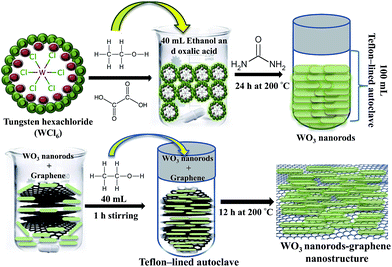 | ||
| Scheme 1 Schematic representation for the preparation of WO3 nanorods and WO3 nanorods–graphene nanostructure. | ||
Optical analysis of the P-graphene and WO3 nanorods–graphene nanostructure
The optical diffuse absorbance/reflectance spectra of the P-graphene and as-prepared WO3 nanorods–graphene nanostructure were measured at room temperature over the wavelength range, 200–800 nm. Fig. 1(a) presents the UV-vis absorption spectra of P-graphene and WO3 nanorods–graphene nanostructure. The absorption peak located at approximately 249.3 nm was assigned to the π–π transition of graphene. The characteristic absorption peak of the WO3 nanorods–graphene nanostructure has been observed at 292.9 nm. The absorption spectra (Fig. 1(a)) show the combined effects of WO3 nanorods and graphene, which contributed to an improved light harvesting property. This is expected to result in improved photocatalytic activity over the visible range. The reflectance peak (Fig. S2†) at 289.4 nm in the case of the WO3 nanorods–graphene nanostructure was assigned to electronic conjugation between the WO3 nanorods and graphene nanosheets, which is similar to previous studies.24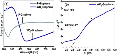 | ||
| Fig. 1 (a) UV-Vis absorbance spectra of P-graphene and WO3 nanorods–graphene, and, (b) Tauc plot for indirect band gap of WO3 nanorods–graphene nanostructure. | ||
The band gap of the as-prepared nanocomposite was calculated (Fig. 1(b)) to be Eg = 2.34 eV using the equation, αhν = A(hν − Eg)1/2, where Eg (eV) is the band gap of the semiconductor, h is Planck's constant, ν is the frequency of light, and A is a constant. These obtained values were in accordance with the literature.24,25
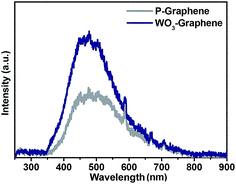
The PL spectra of the WO3 nanorods–graphene nanostructure can help reveal the efficiency of charge carrier trapping, migration and transfer to understand the fate of the electrons and holes in the nanomaterials.24 Fig. 2 shows the PL emission peaks of P-graphene and WO3 nanorods–graphene nanostructure at an excitation wavelength of 325 nm. The PL spectrum of P-graphene shows the similar peak reported in the literature for graphene.13 PL of P-graphene shows the emission peaks at ∼500 nm in the visible light region, which is because of the electronic behaviour of graphene.14 In contrast, the PL intensity of the WO3 nanorods–graphene nanostructure emission peak was increased significantly (Fig. 2). This suggests an additional pathway for electron transfer, i.e. from the conduction band of the excited WO3 to graphene sheets. In general, PL measurements revealed the charge recombination and migration efficiency of the metal and metal oxide nanocomposite, because the photocatalytic activity is associated closely to the PL intensity and the recombination rate of photoexcited electrons and holes. In general, the efficient charge separation and the inhibited electron–hole recombination by WO3 are favourable for enhancing the photo-activity of WO3 nanorods–graphene nanostructure. The PL spectra showed that WO3 nanorods decoration on the P-graphene nanosheets can effectively inhibit electron–hole recombination during visible light irradiation. Our results confirmed the suppression of the recombination of electrons and holes on the surface of the WO3 nanorods–graphene compared to the bare WO3 nanorods.25,26 This is also an indicative of the quantum size, uniform distribution and its interactions with graphene nanosheets. This showed that the size, shape and support of the nanostructured materials may have an effect on their optical properties.
Structural analysis of the P-graphene and WO3 nanorods–graphene nanostructure
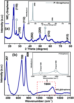
Fig. 3(a) shows the XRD patterns of the P-graphene and WO3 nanorods–graphene nanostructure. All the XRD peaks can be well indexed to the standard diffraction pattern of hexagonal phase of WO3 (JCPDS 89-8052).18 The major XRD peaks from the inset in Fig. 3(a), which were obtained at 26.5° (002) and 54.7° (100), confirmed the presence of graphene. The combined XRD pattern of the WO3 nanorods–graphene nanostructure showed three main peaks at 23.6° (110), 28.2° (102) and 33.6° (112), which was confirmed from the JCPDS 89-8052 values. On the other hand, the diffraction pattern of the WO3 nanorods–graphene nanostructure was shifted slightly and their lattice parameter was changed from that of pure WO3 nanorods according to the previously mentioned values due mainly to the interaction between some oxygen groups of WO3 and graphene nanosheets.24 This clearly illustrates the decoration of WO3 nanorods on the graphene nanosheets and the overall synthesis of the WO3 nanorods–graphene nanostructure. The mean crystallite size of the WO3 nanorods–graphene nanostructure was calculated using the Scherer's formula, D = κλ/β![[thin space (1/6-em)]](https://www.rsc.org/images/entities/char_2009.gif) cos
cos![[thin space (1/6-em)]](https://www.rsc.org/images/entities/char_2009.gif) θ, where κ is the shape factor and has a typical value of ∼0.9, λ is the wavelength (Cu Kα = 0.15405 nm), β is the full width at half maximum of the most intense peak (in radians), and θ is the main peak of P-graphene at 26.53° 2θ and the crystallite size of the most intense peak was 15.8 nm. In contrast, the most intense peak of WO3 nanorods–graphene nanostructure was observed at 23.68° 2θ and the crystallite size was 6.07 nm. This shows that the crystallite size is decreasing due to the decoration/presence of WO3 nanorods at the graphene nanosheets. This further confirmed the successful synthesis of the WO3 nanorods–graphene nanostructure.27,28
θ, where κ is the shape factor and has a typical value of ∼0.9, λ is the wavelength (Cu Kα = 0.15405 nm), β is the full width at half maximum of the most intense peak (in radians), and θ is the main peak of P-graphene at 26.53° 2θ and the crystallite size of the most intense peak was 15.8 nm. In contrast, the most intense peak of WO3 nanorods–graphene nanostructure was observed at 23.68° 2θ and the crystallite size was 6.07 nm. This shows that the crystallite size is decreasing due to the decoration/presence of WO3 nanorods at the graphene nanosheets. This further confirmed the successful synthesis of the WO3 nanorods–graphene nanostructure.27,28
Raman spectroscopy provides valuable information on the electronic and structural properties of carbon materials, such as graphene. Fig. 3(b) shows the Raman spectra of the WO3 nanorods–graphene nanostructure and graphene nanosheets. Both spectra indicated the existence of a G band (∼1595 cm−1), which is related to the C–C vibrations of carbon with a sp2 orbital structure, and the D band (disorder band, ∼1350 cm−1), which is associated with the disorder-induced vibration of the C–C bond. The characteristic peaks of the D and G bands at approximately 1350 cm−1 and 1595 cm−1 were observed. The D band provides information on the breathing mode of the k-point, and the G band is related to the tangential stretching mode of the E2g phonon of the sp2 carbon atoms.28,29 In the Raman spectra of the as-prepared WO3 nanorods–graphene nanostructure, sharp peaks for WO3 at 1604 cm−1, which is shifted slightly from the graphene G band and low-intensity peaks for graphene were also observed. The Raman bands at 709 cm−1 and 809 cm−1 (W–O stretching modes) and 267 cm−1 (W–O bending mode) were characteristic of monoclinic WO3.29–31 Nonaka et al. reported the Raman bands for m-WO3 at 809 and 712 cm−1. These results confirmed the successful formation of the WO3 nanorods–graphene nanostructure material.
FT-IR analysis of P-graphene and WO3 nanorods–graphene nanostructure
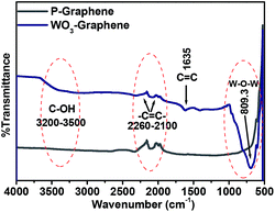
The functional interaction between the WO3 and graphene was also confirmed using FT-IR analysis, as shown in Fig. 4. The stretching frequency of the COH group (3200–3500 cm−1) due to the C–H and O–H stretching vibrations is clearly visible. The spectrum also revealed a peak in the range, 2260–2100 cm−1, which is due to the presence of aromatic –C![[double bond, length as m-dash]](https://www.rsc.org/images/entities/char_e001.gif) C– that usually appear as a number of weak absorptions. The peak at 1635 cm−1 was assigned to the remaining sp2 of –C
C– that usually appear as a number of weak absorptions. The peak at 1635 cm−1 was assigned to the remaining sp2 of –C![[double bond, length as m-dash]](https://www.rsc.org/images/entities/char_e001.gif) C– nature of the material.32 The partial absorption bands between 1300 and 4000 cm−1 are assigned mainly to the chemisorbed and/or physisorbed H2O and CO2 molecules on the surface of the WO3 nanorods–graphene nanostructure. In the case of the WO3 nanorods–graphene bands in the region, 700 cm−1, 1041 cm−1 corresponds to the W–O groups and W–OH groups32,33 which was not observed in the spectrum of P-graphene. This confirms the formation of WO3 nanorods on the surface of the graphene nanosheets.
C– nature of the material.32 The partial absorption bands between 1300 and 4000 cm−1 are assigned mainly to the chemisorbed and/or physisorbed H2O and CO2 molecules on the surface of the WO3 nanorods–graphene nanostructure. In the case of the WO3 nanorods–graphene bands in the region, 700 cm−1, 1041 cm−1 corresponds to the W–O groups and W–OH groups32,33 which was not observed in the spectrum of P-graphene. This confirms the formation of WO3 nanorods on the surface of the graphene nanosheets.
Morphological analysis of WO3 nanorods–graphene nanostructure
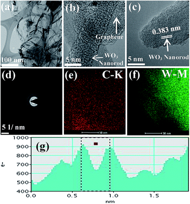
The surface morphology of WO3 nanorods–graphene nanostructure was examined by FE-SEM, as shown in Fig. S3(a and b).† This shows various rod shape structures on the surface of the graphene nanosheets at different scale. This confirmed that the graphene nanosheets are decorated with the WO3 nanorods, which was further confirmed by TEM.The morphology and composition of the WO3 nanorods–graphene nanostructure was confirmed by TEM and EDS. Fig. 5(a) shows that there is an abundance of rod shape structures on the graphene sheet owing to the two-dimensional nature of the matrix sheet. The distribution of WO3 nanorods onto the graphene nanosheets and their intimate contact can be seen clearly from the TEM images. Fig. 5(b) shows a HR-TEM image, which provides direct evidence of WO3 nanorods on the surface of the graphene nanosheets and clearly indicates the interfacial interaction between the WO3 nanorods and graphene nanosheets. Fig. 5(c) shows the lattice-fringe spacing of the WO3 nanorods, which is 0.36 nm. Fig. 5(d) shows the SAED pattern, which revealed the polycrystalline nature of WO3 nanorods-graphene nanostructure. Fig. 5(e) and (f) shows the elemental mapping of C-K and W-M, respectively. Fig. 5(g) shows the line intensity profile obtained from TEM software analysis, showing the plane distance of WO3 nanorods, which is ∼0.36 nm. Fig. S4(a–d)† further shows the clear morphology of WO3 nanorods–graphene nanostructure with different scale. Fig. S5† shows the EDS results of WO3 nanorods–graphene nanostructure at various regions. This further confirms that the WO3 nanorods were successfully present/anchored at the surface of the graphene nanosheets.
XPS analysis of P-graphene and WO3 nanorods–graphene nanostructure
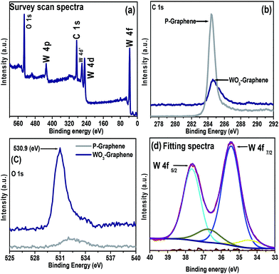
XPS is an effective technique for analysing the surface chemical states and confirm their corresponding valence state.34 Fig. 6(a) shows the survey scan spectra of the WO3 nanorods–graphene nanostructure, in which the peak associated with C 1s and W 4f peak was observed at 284.70 eV and the major W 4f peak was at 36.14 eV.24,34 This provides evidence of the successful anchoring/formation of WO3 nanorods onto the graphene sheets. Fig. 6(b) shows the high resolution spectra for C 1s at the characteristic binding energy (B.E.) of 284.43 eV for P-graphene, whereas for the WO3 nanorods–graphene nanostructure the C 1s was shifted to 284.70 eV B.E., which confirms the successful formation and anchoring of WO3 nanorods onto graphene nanosheets. Fig. 6(c) shows the O 1s peak of P-graphene and the as-prepared WO3 nanorods–graphene nanocomposite at (530.9 eV). In the case of P-graphene, there was a negligible oxygen peak in the spectra compared to the as prepared nanocomposite. The intense oxygen peak can be seen from the spectra of the as-prepared nanocomposite, which shows the oxygenation from the tungsten oxide. Fig. 6(d) shows the high resolution XP spectra of the W 4f peaks for the WO3 nanorods–graphene nanostructure. To examine the chemical state of WO3, there were two major peaks of the W 4f5/2 and W 4f7/2 core levels cantered at 37.60 eV and 35.43 eV. The binding energies of these photoelectron peaks were characteristic of WO3.24 In addition to the oxygen peaks, a W 4f peak was also observed in the WO3 nanorods–graphene nanostructure sample.The atomic weight% of the elements such as, carbon, oxygen and tungsten are mentioned in the Table 1, which is obtained from XPS analysis. The higher atomic weight percent of carbon clearly shows the presence of graphene nanosheets on which WO3 nanorods are decorated. This is attributed to the combined effect of WO3 nanorods and graphene which made an improved performance of WO3 nanorods–graphene nanostructure for photocapacitive and photocatalytic activities.
| No. | Elements | Binding energy (eV) | Atomic weight (%) |
|---|---|---|---|
| 1 | Carbon | 284.43 eV | 52.87 |
| 2 | Oxygen | 530.9 eV | 31.71 |
| 3 | Tungsten W 45/2 and W 47/2 | 37.60 eV, 35.43 eV | 15.42 |
Applications of WO3 nanorods–graphene nanostructure
Cyclic voltammetry (CV) is generally used to examine the capacitive properties and redox nature of the material and it is a type of potentiodynamic electrochemical measurement.33 In CV analysis, the working electrode potential is ramped linearly as a function of time. The photoelectrochemical responses of P-graphene and WO3 nanorods–graphene nanostructure on the surface-modified carbon paper were examined by CV. Fig. 7 shows the CV performance of the P-graphene and WO3 nanorods–graphene nanostructure in the dark and under visible light irradiation in a 0.2 M PBS (pH = 7) solution. The first anodic sweep from 0.8 to −0.8 revealed an oxidation peak of P-graphene at 0.475 V to 0.472 V on the carbon paper surface in the dark and under visible light irradiation. On the other hand, the cathodic sweep from −0.8 to 0.8 revealed a reduction peak of P-graphene at 0.129 V to 0.129 V in the dark and under visible light irradiation. In the case of the WO3 nanorods–graphene nanostructure, the anodic sweep from 0.8 to −0.8, an oxidation peak was observed at 0.473 V to 0.456 V in the dark and under visible light irradiation. On the reverse potential scan from −0.8 to 0.8, a wide oxidation was observed at 0.129 V to 0.134 V in the case of WO3 nanorods–graphene nanostructure in the dark and under visible light irradiation. P-graphene did not show significant much improvement in the oxidation and reduction peaks at scan rates of 0.05 mV s−1, whereas the WO3 nanorods–graphene nanostructure showed well resolved oxidation and reduction peaks.35–37 The large peak separation (ΔEp) was observed in the case of WO3 nanorods–graphene nanostructure, which increases compared to P-graphene. This indicates the improved redox behaviour, which could be due to the presence/decoration of WO3 nanorods at the graphene surface. These observations confirm the enhanced electrochemical behaviour of the WO3 nanorods–graphene nanostructure, which is probably due to the uniform decoration of small WO3 nanorods over the graphene surface.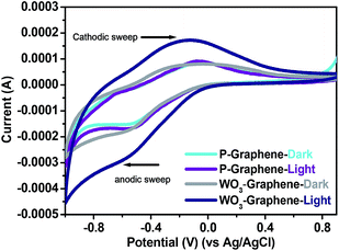 | ||
| Fig. 7 Cyclic voltammetry profile of P-graphene and WO3 nanorods–graphene nanostructure in a 0.2 M phosphate buffer (pH = 7) solution at 25 °C at a scan rate of 0.05 mV s−1. | ||
Calculation of the specific capacitance behaviour of P-graphene and WO3 nanorods–graphene nanostructure under visible light illumination
Fig. 7 shows the cyclic voltammogram of P-graphene and WO3 nanorods–graphene nanostructure in the dark and under visible light irradiation at a scan rate of 0.05 mV s−1. The CV plot of the WO3 nanorods–graphene nanostructure showed the improved positive and negative sweep, indicating their pseudo capacitive nature. The peak current of the WO3 nanorods–graphene nanostructure increased linearly in the dark and under visible light irradiation with a positive shift of the cathodic peak and a negative shift of the anodic peak.From CV, the specific capacitance (Csp) of the electrodes was determined using the following equation:
| Csp = I/[scan rate(dv/dt)VM] | (1) |
The specific capacitance (Csp) of the P-graphene was measured in the dark and under visible light irradiation to be 7.43 F g−1 and 7.76 F g−1 at a current density of 5 mA g−1, while the capacitance of the WO3 nanorods-graphene nanostructure was 64.2 F g−1 and 121.4 F g−1. The as-prepared nanocomposite exhibited enhanced specific capacitance in comparison with the P-graphene. This was attributed due to the highly conductive nature of graphene, which facilitated the charge transfer in WO3 nanorods–graphene nanostructure, and ensure high electrochemical utilization of graphene with WO3 nanorods.17,37,38
Photocatalytic degradation evaluation of the organic model dye using P-graphene and WO3 nanorods–graphene nanostructures under visible light irradiation
The photocatalytic activity of the WO3 nanorods–graphene nanostructure was compared with that of P-graphene, which was evaluated by degrading the MB as a model pollutant dye. As shown in Fig. 8, P-graphene showed significantly much lower photocatalytic degradation performance than the WO3 nanorods–graphene nanostructure, which shows the enhanced performance of WO3 nanorods–graphene as a nanocomposite for improving the photocatalytic activity. The efficient charge separation and transfer appears responsible for the enhanced photocatalytic activity of the WO3 nanorods–graphene nanostructure. Graphene has a high surface area and charge-carrier mobility of 200000 cm2 V−1 s−1 at room temperature, suggesting that the incorporation of WO3 nanorods onto graphene nanosheets which plays an important role in enhancing the charge separation efficiency and suppressing charge recombination, as suggested in Fig. 9. Under visible light irradiation, electrons (e−) and holes (h+) are generated in the WO3 nanorods. On the other hand, photogenerated electrons can be transferred to carbon atoms in the graphene nanosheets and then react with the organic pollutant to reduce the recombination of electron–hole pairs. This is because graphene served as an electron sink/acceptor of electrons generated in the WO3 nanorods and effectively decreased the recombination probability of the electron–hole pairs.39,40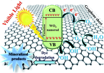 | ||
| Fig. 9 Electron transfer mechanism for the photocatalytic degradation of organic pollutant using WO3 nanorods–graphene nanostructure under visible light irradiation. | ||
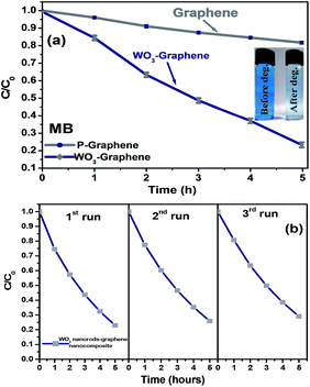
Fig. 8(a) shows the photocatalytic degradation (C/C0) of MB as a function of the irradiation time. Here, C is the absorption of MB at each time interval of irradiation, and C0 is the absorption of the initial concentration (time 0). The photocatalytic performance of graphene nanosheets as a photocatalyst was recorded only ∼16%, whereas, in case of WO3 nanorods–graphene nanostructure the observed photocatalytic performance was ∼80% for MB in 5 h under visible light irradiation. This suggests that the WO3 nanorods anchored at the surface of the graphene nanosheets enhanced the photocatalytic activity of graphene for effective pollutant degradation under visible light irradiation.
The stability and reusability test of the nanomaterials is the prime concern. Therefore, stability and reusability test of the as prepared photocatalysts was performed. The stability test (Fig. S1†) showed that the WO3 nanorods–graphene nanostructure is quite stable. The photodegradation of MB was repeated for three cycles, each for 5 h. After each cycle, the WO3 nanorods–graphene was centrifuged and the optical absorption was measured using a UV-Vis spectrometer. As shown in Fig. 8(b), ∼80% of the photocatalytic activity was retained, revealing the good reusability of the as-prepared nanocomposite as a photocatalyst. This showed that the WO3 nanorods–graphene had not been deactivated significantly and quite stable.
Proposed mechanism of the enhanced photocatalysis for the photodegradation of MB using WO3 nanorods–graphene nanostructure under visible light irradiation
Generally, an increase in the absorptivity of pollutants enhances light absorption, and efficient charge separation, recombination and transfer plays an important role in the improved photocatalytic activity of the photocatalyst. The photocatalytic activity of the photocatalyst depends on the reducing and oxidizing ability of the photoelectrons and holes generated under visible light irradiation.39,40In general, a Schottky barrier is formed when two materials with different work functions are combined and electrons are transferred from the material with a lower work function to a material with a higher work function until the two levels reach equilibrium to form a new Fermi energy level.40,41 The equilibrium alignment of the Fermi level of the metal oxide and graphene nanocomposite materials creates a built-in electric field in the space charge region near the interface, which promotes the separation of photogenerated electrons and holes, and improves the photocatalytic activity.41 As shown in the proposed reaction mechanism (Fig. 9), under visible light irradiation, the graphene acts as an electron-acceptor material that hinder the electron–hole pair recombination. The feature of 1-D single crystalline WO3 nanorods provided another possible electron pathway between WO3 and coupled graphene nanosheets, which formed more reactive sites for the degradation of the dyes on the surface of both graphene and WO3 nanorods. Therefore, the WO3 nanorods–graphene nanostructure showed superior photocatalytic activity as compared to P-graphene under visible light irradiation.40–42
Conclusions
High-density WO3 nanorods were synthesized and deposited on the graphene nanosheets using a simple hydrothermal method and characterized using standard techniques. The carbon paper modified by the resulting WO3 nanorods–graphene nanostructure was used to measure the photocapacitive behaviour and it showed enhanced photocapacitive behaviour as compared to P-graphene. The good electrochemical performance for the WO3 nanorods–graphene nanostructure may be attributed to the interaction between the WO3 nanorods and the edges of graphene nanosheets, which increases the ion diffusion rate as well as the conductivity. The essential merits of the photocatalyst include using graphene as a carrier or promoter and its potential use for the development of next-generation photocatalyst systems. Therefore, the as-prepared WO3 nanorods–graphene nanostructure was used as an efficient photocatalyst for the photocatalytic degradation of organic model pollutant and it showed three fold higher performance than P-graphene nanosheets. The improved and enhanced photocapacitive and photocatalytic performances of the WO3 nanorods–graphene nanostructure was achieved because of the decoration of the WO3 nanorods on the graphene nanosheets. Hence, this type of nanostructure, which is capable of utilizing the perfect photocapacitive behaviour and exhibit efficient photocatalytic behaviour for the removal of organic pollutants from the waste water treatment, would be the accurate choice in the near future for a range of possible novel applications.Acknowledgements
This study was supported by Priority Research Centres Program (Grant No. 2014R1A6A1031189), and by Basic Science Research Program (Grant No. 2015R1D1A3A03018029) through the National Research Foundation of Korea (NRF) funded by the Ministry of Education.References
- R. Abe, J. Photochem. Photobiol., C, 2010, 11, 179–209 CrossRef CAS
.
- N. Zhang, S. Liu, X. Fu and Y. J. Xu, J. Phys. Chem. C, 2011, 115, 22901–22909 CAS
.
- R. P. Sajanlal, S. T. Sreeprasad, K. A. Samal and T. Pradeep, Nano Rev., 2011, 2, 5883–25945 Search PubMed
.
- H. Liu, N. Gao, M. Liao and X. Fang, Sci. Rep., 2015, 5, 7716–7725 CrossRef CAS PubMed
.
- F. Zheng, M. Guo and M. Zhang, CrystEngComm, 2013, 15, 277–284 RSC
.
- Y. D. Wang, Z. X. Chen, Y. F. Li, Z. L. Zhou and X. H. Wu, Solid-State Electron., 2001, 45, 639–644 CrossRef CAS
.
- Z. D. Meng, L. Zhu, J. G. Choi, C. Y. Park and W. C. Oh, Nanoscale Res. Lett., 2011, 6, 459–470 CrossRef PubMed
.
- M. Qamar, Q. Drmosh, M. I. Ahmed, M. Qamaruddin and Z. H. Yamani, Nanoscale Res. Lett., 2015, 10, 54–60 CrossRef PubMed
.
- S. S. Kalanur, Y. J. Hwang, S. Y. Chae and O. S. Joo, J. Mater. Chem. A, 2013, 1, 3479–3488 CAS
.
- J. Byun, J. Microbiol. Biotechnol., 2015, 25, 145–151 CrossRef CAS PubMed
.
- F. Bonaccorso, Z. Sun, T. Hasan and A. C. Ferrari, Nat. Photonics, 2010, 4, 611–622 CrossRef CAS
.
- Z. Yang, R. Gao, N. Hu, J. Chai, Y. Cheng, L. Zhang, H. Wei, E. S. W. Kong and Y. Zhang, Nano-Micro Lett., 2012, 4, 1–9 CrossRef
.
- M. E. Khan, M. M. Khan and M. H. Cho, RSC Adv., 2015, 5, 26897–26904 RSC
.
- M. E. Khan, M. M. Khan and M. H. Cho, New J. Chem., 2015, 39, 8121–8129 RSC
.
- Y. Wang, H. Chang, H. Wu and H. Liu, J. Mater. Chem. B, 2013, 1, 3521–3534 RSC
.
- X. Gan and H. Zhao, Sens. Mater., 2015, 27, 191–215 CAS
.
- Y. Cai, Y. Wang, S. Deng, G. Chen, Q. Li, B. Han, R. Han and Y. Wang, Ceram. Int., 2014, 40, 4109–4116 CrossRef CAS
.
- S. Thangave, M. Elayaperumal and G. Venugopal, Mater. Express, 2012, 2, 327–334 CrossRef
.
- Z. Dimitrova and D. Gogova, Mater. Res. Bull., 2005, 40, 333–340 CrossRef CAS
.
- X. Chang, L. Dong, Y. Yin and S. Sun, RSC Adv., 2013, 3, 15005–15013 RSC
.
- A. Adán-Más and D. Wei, Nanomaterials, 2013, 3, 325–356 CrossRef
.
- W. Lu, J. Chen, Y. Wu, L. Duan, Y. Yang and X. Ge, Nanoscale Res. Lett., 2014, 9, 148–155 CrossRef PubMed
.
- X. Han, X. Han, L. Li and C. Wang, New J. Chem., 2012, 36, 2205–2208 RSC
.
- X. An, J. C. Yu, Y. Wang, Y. Hu, X. Yu and G. Zhang, J. Mater. Chem., 2012, 22, 8525–8531 RSC
.
- P. P. González-Borrero, F. Sato, A. N. Medina, M. L. Baesso, A. C. Bento, G. Baldissera, C. Persson, G. A. Niklasson, C. G. Granqvist and A. Ferreira da Silva, Appl. Phys. Lett., 2010, 96, 061909–061912 CrossRef
.
- K. Krishnamoorthy, M. Veerapandian, R. Mohan and S. J. Kim, Appl. Phys. A, 2012, 106, 501–506 CrossRef CAS
.
- W. Wu, Q. Yu, J. Lian, J. Bao, Z. Liu and S. S. Pei, J. Cryst. Growth, 2010, 312, 3147–3150 CrossRef CAS
.
- S. Srivastava, K. Jain, V. N. Singh, S. Singh, N. Vijayan, N. Dilawar, G. Gupta and T. D. Senguttuvan, Nanotechnology, 2012, 23, 205501–205508 CrossRef PubMed
.
- S. Stankovich, D. A. Dikin, R. D. Piner, K. A. Kohlhaas, A. Kleinhammes, Y. Jia, Y. Wu, S. T. Nguyen and R. S. Ruoff, Carbon, 2007, 45, 1558–1565 CrossRef CAS
.
- Z. Lu, S. M. Kanan and C. P. Tripp, J. Mater. Chem., 2002, 12, 983–989 RSC
.
- J. R. Sohn, H. S. Cho and H. W. Kim, J. Ind. Eng. Chem., 1999, 5, 1–9 CAS
.
- U. O. Krašovec, A. S. Vuk and B. Orel, Electrochim. Acta, 2001, 46, 1921–1929 CrossRef
.
- M. M. Khan, S. A. Ansari, J. Lee and M. H. Cho, J. Ind. Eng. Chem., 2013, 19, 1845–1850 CrossRef CAS
.
- S. M. Kanan, Z. Hixiang Lu, J. K. Cox, G. Bernhardt and C. P. Tripp, Langmuir, 2002, 18, 1707–1712 CrossRef CAS
.
- S. M. F. Shaikh, S. S. Kalanur, R. S. Mane and O. S. Joo, Dalton Trans., 2013, 42, 10085–10088 RSC
.
- Y. Liu, Y. Jiao, H. Zhou, X. Yu, F. Qu and X. Wu, Nano-Micro Lett., 2015, 7, 12–16 CrossRef CAS
.
- J. Rajeswari, P. S. Kishore, B. Viswanathan and T. K. Varadarajan, Nanoscale Res. Lett., 2007, 2, 496–503 CrossRef CAS
.
- M. Yu, H. Sun, X. Sun, F. Lu, T. Hu, G. Wang, H. Qiu and J. Lian, Mater. Lett., 2013, 108, 29–32 CrossRef CAS
.
- S. Li, Z. Zhao, Y. Huang, J. Di, Y. (Alec) Jia and H. Zheng, J. Mater. Chem. A, 2015, 3, 5467–5473 CAS
.
- M. Zhou, J. Yan and P. Cui, Mater. Lett., 2012, 89, 258–261 CrossRef CAS
.
- M. M. Khan, S. A. Ansari, M. E. Khan, M. O. Ansari, B. K. Min and M. H. Cho, New J. Chem., 2015, 39, 2758–2766 RSC
.
- S. Chowdhury and R. Balasubramanian, Appl. Catal., B, 2014, 160, 307–324 CrossRef
.
Footnote |
| † Electronic supplementary information (ESI) available. See DOI: 10.1039/c5ra24575c |
| This journal is © The Royal Society of Chemistry 2016 |

