
Copper borate as a photocathode in p-type dye-sensitized solar cells†
Tengfei Jianga,
Martine Bujoli-Doeuffa,
Yoann Farréb,
Errol Blartb,
Yann Pellegrinb,
Eric Gautrona,
Mohammed Boujtitab,
Laurent Cario*a,
Fabrice Odobel*b and
Stéphane Jobic*a
aInstitut des Matériaux Jean Rouxel (IMN), Université de Nantes, CNRS, 2 rue de la Houssinière, BP 32229, 44322 Nantes, Cedex 03, France. E-mail: Stephane.Jobic@cnrs-imn.fr; Laurent.Cario@cnrs-imn.fr
bChimie et Interdisciplinarité: Synthèse, Analyse, Modélisation (CEISAM), Université de Nantes, CNRS, 2 rue de la Houssinière, 44322 Nantes, Cedex 03, France. E-mail: Fabrice.Odobel@univ-nantes.fr
First published on 18th December 2015
Abstract
p-Type dye-sensitized solar cells (p-DSSCs) have recently become a major research focus because coupling with n-type DSSCs yields highly efficient tandem DSSCs. Indeed many delafossite-like compounds appear as promising candidates for p-DSSCs due to their deep valence band position and high hole mobility. In this paper, the synthesis of CuBO2 was attempted by a facile sol–gel methodology. Then, the as-obtained particles were used to prepare photocathodes for p-DSSCs with DPP-NDI dye as sensitizer and tris(4,4′-di-tert-butyl-2,2′-bipyridine)cobalt(III/II) as redox mediator. Due to the deeper valence band position compared with classical NiO photocathode, the “CuBO2” based p-DSSC presents an open-circuit photovoltage (Voc) of 453 mV, which is 150 mV higher than that of NiO in the same conditions. The results show that “CuBO2” is a potential alternative for NiO in p-DSSCs.
In traditional n-type semiconductor (SC) based dye-sensitized solar cells (DSSCs), the photocurrent results from electron injection of the photoexcited dye into the conduction band (CB) of the n-type SCs.1,2 Conversely, in p-type semiconductor based DSSCs, the inverse principle is at work, i.e. holes are injected from the photo-excited dye into the valence band (VB) of the p-type SC. To achieve higher energy conversion efficiency, an attractive strategy is to construct tandem DSSCs, in which an n-type photoanode is coupled with a p-type photocathode.3 Until now, the energy conversion efficiency of p-DSSCs is much lower than that of n-DSSCs (generally a few tenths of percent vs. about 15%), and this mismatch limits the final energy conversion of tandem cells.4 This drawback has prompted the development of better performing photocathodes with new p-SCs, in particular to reach higher photopotentials.4–6 Very recently, Perera et al.7 have investigated NiO based p-DSSCs with an energy conversion efficiency of 2.51%, which is the highest reported efficiency for a p-DSSC so far. This breakthrough clearly results from the use of a new redox mediator ([Fe(acac)3]0/1−) with a very negative redox potential rather than a p-type semiconductor with a deeper valence band. Unfortunately, such an approach would not be effective in the context of the tandem cell concept where the open-circuit photovoltage (Voc) is related to the position of the quasi-Fermi levels of the photoanode and the photocathode, i.e. the difference in energy between the bottom of the CB of n-SC and the top of the VB of p-SC.3,4
The valence band position of NiO is as low as +0.50 V vs. NHE (at pH 7),8 which limits the Voc of p-DSSCs and consequently of the tandem DSSCs. Besides, the photocurrent of NiO based p-DSSCs is restricted by its low hole mobility.9 Accordingly, the development of new p-type semiconductors with deep VB has become a priority. Delafossite oxides are promising candidates owing to their high transparency and conductivity.10 More importantly, in Cu(I)-based delafossite materials, Cu 3d orbitals strongly hybridize with the O 2p orbitals, making the hole charge carriers (related to a slight off-stoichiometry) to be delocalized both on oxygen and copper atoms.11 This facilitates the hole mobility and subsequently, should minimize electron–hole recombinations at the dye/p-SC interfaces due to a regular charge flow from the surface to the interior of the nanoparticles. Several works on CuGaO2, CuCrO2, and CuAlO2 based p-DSSCs were reported recently.9,10 Under AM 1.5 illumination, Voc of 375 mV,12 145 mV13 and 333 mV14 were reached for the gallium, chromium and aluminum derivatives, with respectively the following dye and redox mediator couples: PMI-NDI and Co3+/Co2+, coumarin 343 and I2/I−, and PMI-6T-TPA and I2/I−. These values are much higher than the Voc of 285 mV, 90 mV, and 218 mV measured for NiO based DSSCs prepared in similar conditions.
To the best of our knowledge, there is no report on CuBO2 based p-DSSCs. Yet, in the ABO2 series, boron is a valuable alternative to Al, Cr or Ga. Based on the investigations of Snure and Tiwari15 on thin films, the hole mobility of CuBO2 is 100 cm2 V−1 s−1 which is much higher than that of CuAlO2 (10 cm2 V−1 s−1),11 CuGaO2 (0.2 cm2 V−1 s−1),16 and CuCrO2 (0.2 cm2 V−1 s−1).17 Then CuBO2 appears at first sight as a very good candidate for p-DSSCs.
Herein, we report on the synthesis and characterization of CuBO2 particles and their subsequent use to fabricate p-DSSC exhibiting a higher Voc than conventional NiO-based DSSCs with the same dye and electrolyte.
The CuBO2 particles were synthesized by the sol–gel method of Santra et al.18 Typically, soluble copper(II) nitrate trihydrate and boric acid were used as precursors, which were dissolved in water and nitric acid, respectively. Then citric acid was added in the mixed solution of the precursors to generate the gel. After sintering the gel under air at 550 °C, dark green CuBO2 particles were obtained. More details are given in the ESI.†
Powdered CuBO2 samples were first analyzed by XRD. The XRD pattern, displayed in Fig. 1, gathers the characteristic peaks of CuBO2, i.e. contributions at 32.4, 35.4, 38.6, 48.7, 53.3, and 58.1° in 2θ assigned to (006), (100), (012), (106), (107), and (018) planes by Snure and Tiwari,15 Santra et al.19,20 and Ruttanapun21 for a rhombohedral structure with a and c parameters of about 2.84 Å and 16.52 Å, respectively. Unfortunately, any attempt to refine the XRD pattern via the Rietveld analysis based on CuBO2 material with the delafossite structure type, i.e. a structure built upon edge-sharing (BO6) octahedra defining infinite 2/∞[BO2] layers linked to each other by Cu cations in dumbbell coordination22 (space group (SG): R![[3 with combining macron]](https://www.rsc.org/images/entities/char_0033_0304.gif) m) was not successful. Thus, even if reported in many articles, the real existence of CuBO2 with a delafossite structure type is highly questionable. This issue was initially raised by Cerqueira et al.23 who first witnessed the improbability of the reported structure type for CuBO2. From ab initio calculations, they allege that the ground state of the aforementioned material would correspond to a layered structure with triangular coordinated boron in 2/∞ [BO2] layers separated by Cu in linear coordination forming infinite 1/∞ [CuO] zigzag chains (SG: Cc, a = 3.63 Å, b = 12.45 Å, c = 4.42 Å, β = 86.78°). Two other metastable structures, a tetragonal one (SG: I
m) was not successful. Thus, even if reported in many articles, the real existence of CuBO2 with a delafossite structure type is highly questionable. This issue was initially raised by Cerqueira et al.23 who first witnessed the improbability of the reported structure type for CuBO2. From ab initio calculations, they allege that the ground state of the aforementioned material would correspond to a layered structure with triangular coordinated boron in 2/∞ [BO2] layers separated by Cu in linear coordination forming infinite 1/∞ [CuO] zigzag chains (SG: Cc, a = 3.63 Å, b = 12.45 Å, c = 4.42 Å, β = 86.78°). Two other metastable structures, a tetragonal one (SG: I![[4 with combining macron]](https://www.rsc.org/images/entities/char_0034_0304.gif) m2, a = 2.54 Å, c = 10.82 Å) and an orthorhombic one (SG: Cmc21, a = 2.57 Å, b = 11.67 Å, c = 4.51 Å), both with tetrahedral coordinated boron, were predicted as more stable than the common P63/mmc or Rm delafossite structures. Attempts to refine the collected XRD pattern with all these structures were not successful, as well as trials with the wurtzite-derived β-NaFeO2-structure type, recently stabilized via soft chemistry route by Omata et al.24 for CuGaO2. Thus, at this stage the CuBO2 structure has to be viewed as non-identified, in contradiction with many reports in the literature. A more accurate examination of the XRD pattern, followed by a Rietveld refinement, even led to the assignment of the aforementioned well defined peaks to CuO, i.e. a monoclinic system with a = 4.6741(19) Å, b = 3.4307(15) Å, c = 5.1295(23) Å and β = 99.33(3). This clearly means that the XRD peaks commonly attributed to CuBO2 with a delafossite structure type belong in fact to the CuO phase. On the other hand, chemical analyses by Inductively Coupled Plasma Optical Emission Spectrometry (ICP-OES) clearly attest the presence of boron with a Cu
m2, a = 2.54 Å, c = 10.82 Å) and an orthorhombic one (SG: Cmc21, a = 2.57 Å, b = 11.67 Å, c = 4.51 Å), both with tetrahedral coordinated boron, were predicted as more stable than the common P63/mmc or Rm delafossite structures. Attempts to refine the collected XRD pattern with all these structures were not successful, as well as trials with the wurtzite-derived β-NaFeO2-structure type, recently stabilized via soft chemistry route by Omata et al.24 for CuGaO2. Thus, at this stage the CuBO2 structure has to be viewed as non-identified, in contradiction with many reports in the literature. A more accurate examination of the XRD pattern, followed by a Rietveld refinement, even led to the assignment of the aforementioned well defined peaks to CuO, i.e. a monoclinic system with a = 4.6741(19) Å, b = 3.4307(15) Å, c = 5.1295(23) Å and β = 99.33(3). This clearly means that the XRD peaks commonly attributed to CuBO2 with a delafossite structure type belong in fact to the CuO phase. On the other hand, chemical analyses by Inductively Coupled Plasma Optical Emission Spectrometry (ICP-OES) clearly attest the presence of boron with a Cu![[thin space (1/6-em)]](https://www.rsc.org/images/entities/char_2009.gif) :B ratio of 1.15:1. This perfectly agrees with the ratio reported by Santra et al. determined from EDX investigations19,20 that ranges from 1.03 to 1.35. Moreover, measurements by X-ray photoelectron spectroscopy (XPS, Fig. S1†) reveal the presence of CuI and CuII cations at the surfaces. All these measurements suggest therefore that our product is composed of a “CuBO2” majority phase with an amorphous character which is mixed with a small amount of cupric oxide.
:B ratio of 1.15:1. This perfectly agrees with the ratio reported by Santra et al. determined from EDX investigations19,20 that ranges from 1.03 to 1.35. Moreover, measurements by X-ray photoelectron spectroscopy (XPS, Fig. S1†) reveal the presence of CuI and CuII cations at the surfaces. All these measurements suggest therefore that our product is composed of a “CuBO2” majority phase with an amorphous character which is mixed with a small amount of cupric oxide.
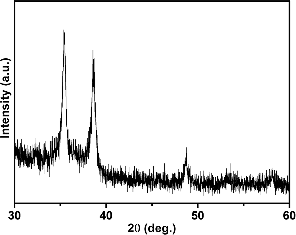 | ||
| Fig. 1 XRD pattern of dark green “CuBO2” prepared by sol–gel method annealed at 550 °C for 1 h under air. | ||
In order to verify this assumption our prepared material was examined with a transmission electron microscope (TEM). The TEM micrographs displayed in Fig. 2a and b, clearly evidence the existence of well faceted crystals embedded in a gangue with a granular texture. From the electron diffraction (Fig. 2c), the crystals can be ascribed to CuO. The gangue, which would correspond to more than ∼90% in volume of the sample, turns to be very reactive under the electron beam at room temperature and requires low temperature (−180 °C) to be examined. This gangue reveals an electron diffraction pattern of a poorly crystallized phase (see Fig. 2d) and likely corresponds to an “amorphous” phase of CuBO2.
 | ||
| Fig. 2 (a) and (b) Room temperature TEM image of our prepared sample with CuO crystal in dark and the “CuBO2” gangue in bright. (c) and (d) Selected area electron diffraction patterns of CuO and “CuBO2”. | ||
Room temperature Raman spectrum of “CuBO2” was collected and compared to that of CuO, Cu2O and B2O3, three binary phases that might be present as sub-products (see Fig. 3). Namely, in the 100–1400 cm−1 range, six well defined vibration modes at 142, 196, 282, 719, 958, and 1248 cm−1 are observed for “CuBO2”. In addition, two featured broad massifs are located in the 420–520 cm−1 and 1100–1200 cm−1 regions. Peaks at 196 cm−1 and 719 cm−1 exhibit analogies with peaks observed in delafossite materials and could correspond to pseudo Ag (205 cm−1, 213 cm−1 for CuCrO2 and CuGaO2) and A1g (707 cm−1, 738 cm−1 for CuCrO2 and CuGaO2) modes, respectively.25–27 Others peaks are unexplained. Nevertheless, it is clear that the Raman spectrum of “CuBO2” is significantly different to those of CuO, Cu2O and B2O3. Consequently, if present, we may suppose that these secondary phases have to be viewed as minor impurities in agreement with our TEM analysis.
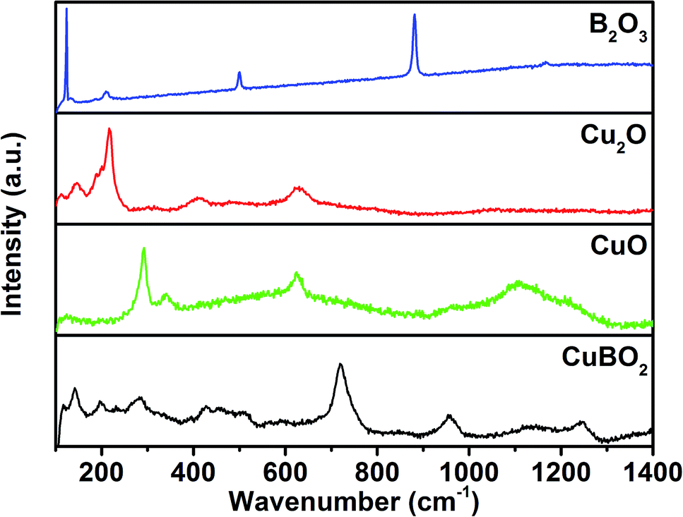 | ||
| Fig. 3 Room temperature Raman spectrum of “CuBO2” CuO, Cu2O, and B2O3 under excitation at 514 nm. | ||
The thermal stability of “CuBO2” was studied by TGA-DTA as shown in Fig. 4. Below 400 °C, the weight loss originates from the departure of physically and chemically adsorbed water molecules on the surface, which generates two peaks in heat flow curve at 100 and 220 °C. Above 600 °C, the phase Cu3B2O6 (JCPDS 28-0398) is generated as confirmed by XRD (see Fig. S2 in the ESI†). This confirms the presence of a large amount of Boron in our amorphous “CuBO2” powder. The oxidation of “CuBO2” may then occur in air according to the reactions.
| 12CuBO2 + 3O2 → 4Cu3B2O6 + 2B2O3 |
| 4CuBO2 + 2CuO + O2 → 2Cu3B2O6 |
 | ||
| Fig. 4 TGA and DSC curves of CuBO2 as prepared under air atmosphere. | ||
Due to the low melting point of B2O3 (450 °C), no diffraction peaks of B2O3 are identified in Fig. S2.† Thus, CuBO2 clearly behaves differently with other delafossite materials which commonly transit towards a spinel phase under heating in air.28 The specific surface area of our as-prepared “CuBO2” material determined by Brunauer–Emmett–Teller (BET) method is 18.5(1) m2 g−1 (i.e. a much lower value than the one of Inframat® NiO (151.9(5) m2 g−1) used as reference in the following). This value also turns to be lower than that of CuCrO2 and CuGaO2 prepared by hydrothermal synthesis.29,30
The transformed Kubelka–Munk reflectance spectrum of “CuBO2” and NiO is given in Fig. S3† and agrees with the dark green color of the material since absorptions in the red and blue regions of the visible range take place. UV-vis transmittance spectrum of CuBO2 film prepared by screen printing and sintered at 350 °C for 60 min for using in p-DSSC (see ESI† for details) is shown in Fig. 5. The film has a good transmittance in visible region and its transparence is not affected by the presence of CuO in small amount.
 | ||
| Fig. 5 Transmittance spectrum of “CuBO2” film on FTO substrate prepared by screen printing and sintered at 350 °C for 60 min under air. The thickness of the film is ∼1 μm. | ||
To determine the VB position of CuBO2 the electrochemical impedance spectroscopy (EIS) measurement was carried out (see ESI† for details), in which the Mott–Schottky plot was extracted at 1 kHz as shown in Fig. 6a. The negative slope of the plot confirms the p-type semiconductivity of “CuBO2”. The flat band potential was determined from the intercept of the axis with potential values, which is 0.31 V (vs. SCE) for CuBO2 at pH 9.4. Consequently, there is a 0.2 V positive shift compared to that of NiO measured (Fig. 6b) in the same conditions (and a 0.16 V shift compared to CuO).31 The flat band potential (FBP) of “CuBO2” is quite similar to that of other delafossite compounds. Hence, FBP of CuAlO2 (0.49 V vs. Ag/AgCl at pH 7.2)32 and CuGaO2 (0.49 V vs. SCE at pH 6.3)12 are extrapolated to be ∼0.31 V and ∼0.47 V vs. SCE at pH of 9.4, respectively, when taking into account the difference of the reference electrodes and the pH values. Since the Voc is equal to the difference of the quasi-Fermi level close to the VB and redox potential of electrolyte, a higher Voc is therefore expected for “CuBO2” based p-DSSCs compared to NiO based p-DSSCs. We can also notice that the carrier density calculated from the slope of Mott–Schottky plots is 3.07 × 1013 cm−3 for CuBO2 and 5.00 × 1016 cm−3 for NiO (see ESI† for details).
 | ||
| Fig. 6 (a) Flat band potential of CuBO2 and (b) NiO in 1 M LiClO4 at pH 9.4. | ||
Next, mesoporous films were deposited on FTO glass by screen printing using a paste made of “CuBO2” particles (see ESI† for details). The film was sintered at 350 °C under air atmosphere for 1 h to eliminate the organic components of the used ink and favour a good adhesion of the mineral on the substrate. The dye DPP-NDI33 was used as sensitizer and the redox mediator was tris(4,4′-di-tert-butyl-2,2′-bipyridine)cobalt(III/II)34 (Fig. S4 and S5†). The photovoltaic performances of the solar cells made with “CuBO2” and NiO cathodes in the same conditions are gathered in Table 1. Clearly, the Voc of 453 mV recorded with “CuBO2” is 150 mV higher than that of NiO based solar cell (Fig. 7). This is a direct consequence of the higher flat band potential of “CuBO2” compared to NiO. On the other hand, the short-circuit current (Jsc) is lower than that of NiO. This may be explained by the much lower specific surface area of “CuBO2” film prepared so far compared to that of NiO leading to a much lower dye loading, and consequently a lower capability to absorb light (see Fig. S6†). We would like to also emphasis that the carrier density of CuBO2 is much lower than that of NiO limiting thus the Jsc value. In spite of this, the dark current of CuBO2 based p-DSSC is about 0.7 μA cm−2 at V = 0 (vs. 1.9 μA cm−2 for NiO-based DSSC) which confirms that the photocurrent comes from hole injection from DPP-NDI dye into the valence band of CuBO2.
| Material | Voc (mV) | Jsc (mA cm−2) | FF (%) | η (%) |
|---|---|---|---|---|
| CuBO2 | 453 | 0.02 | 41 | 0.0036 |
| NiO | 305 | 0.31 | 29 | 0.0276 |
 | ||
| Fig. 7 Photovoltage–photocurrent curves under AM 1.5 illumination (1000 W m−2) and dark current curves of solar cells constructed from CuBO2 (a) and NiO (b). | ||
Conclusions
In summary, we have synthesized a “CuBO2” powder as reported in the literature. This material described in many reports as a delafossite corresponds actually to an unknown amorphous “CuBO2” phase containing a small amount of crystallized CuO impurity. This amorphous “CuBO2” powder revealed a p-type character and a flat band potential of 0.31 V vs. SCE at a pH of 9.4. By using this powder, DPP-NDI dye as sensitizer and tris(4,4′-di-tert-butyl-2,2′-bipyridine)cobalt(III/II) as redox mediator, we have fabricated CuBO2 based p-DSSCs. They exhibit a high Voc of 450 mV, which is 150 mV higher compared to NiO based p-DSSCs. Accordingly, CuBO2 is a promising candidate to fabricate higher performing p-DSSCs, and the investigation is under away to increase the specific surface area of this material.Acknowledgements
For financial support, we are grateful to the agency ANR-Progelec via program POSITIF (No. ANR-12-PRGE-0016-01). The authors thank Prof. A. Barnabé from Toulouse for fruitful discussions.Notes and references
- A. Hagfeldt, G. Boschloo, L. Sun, L. Kloo and H. Pettersson, Chem. Rev., 2010, 110, 6595–6663 CrossRef CAS PubMed.
- M. Grätzel, J. Photochem. Photobiol., C, 2003, 4, 145–153 CrossRef.
- A. Nattestad, A. J. Mozer, M. K. R. Fischer, Y.-B. Cheng, A. Mishra, P. Bauerle and U. Bach, Nat. Mater., 2010, 9, 31–35 CrossRef CAS PubMed.
- F. Odobel and Y. Pellegrin, J. Phys. Chem. Lett., 2013, 4, 2551–2564 CrossRef CAS.
- F. Odobel, Y. Pellegrin, E. A. Gibson, A. Hagfeldt, A. L. Smeigh and L. Hammarström, Coord. Chem. Rev., 2012, 256, 2414–2423 CrossRef CAS.
- F. Odobel, L. le Pleux, Y. Pellegrin and E. Blart, Acc. Chem. Res., 2010, 43, 1063–1071 CrossRef CAS PubMed.
- I. R. Perera, T. Daeneke, S. Makuta, Z. Yu, Y. Tachibana, A. Mishra, P. Bäuerle, C. A. Ohlin, U. Bach and L. Spiccia, Angew. Chem., Int. Ed., 2015, 54, 3758–3762 CrossRef CAS PubMed.
- J. He, H. Lindström, A. Hagfeldt and S.-E. Lindquist, J. Phys. Chem. B, 1999, 103, 8940–8943 CrossRef CAS.
- L. D'Amario, L. J. Antila, B. Pettersson Rimgard, G. Boschloo and L. Hammarström, J. Phys. Chem. Lett., 2015, 6, 779–783 CrossRef PubMed.
- M. Yu, T. I. Draskovic and Y. Wu, Phys. Chem. Chem. Phys., 2014, 16, 5026–5033 RSC.
- H. Kawazoe, M. Yasukawa, H. Hyodo, M. Kurita, H. Yanagi and H. Hosono, Nature, 1997, 389, 939–942 CrossRef CAS.
- A. Renaud, B. Chavillon, L. le Pleux, Y. Pellegrin, E. Blart, M. Boujtita, T. Pauporte, L. Cario, S. Jobic and F. Odobel, J. Mater. Chem., 2012, 22, 14353–14356 RSC.
- D. Xiong, Z. Xu, X. Zeng, W. Zhang, W. Chen, X. Xu, M. Wang and Y.-B. Cheng, J. Mater. Chem., 2012, 22, 24760–24768 RSC.
- A. Nattestad, X. Zhang, U. Bach and Y.-B. Cheng, J. Photonics Energy, 2011, 1, 011103 CrossRef.
- M. Snure and A. Tiwari, Appl. Phys. Lett., 2007, 91, 092123 CrossRef.
- T. Mine, H. Yanagi, K. Nomura, T. Kamiya, M. Hirano and H. Hosono, 5th Int. Symp. Transparent Oxide Thin Films Electron. Opt., 2008, vol. 516, pp. 5790–5794 Search PubMed.
- A. Barnabe, Y. Thimont, M. Lalanne, L. Presmanes and P. Tailhades, J. Mater. Chem. C, 2015, 3, 6012–6024 RSC.
- S. Santra, N. S. Das and K. K. Chattopadhyay, Mater. Lett., 2013, 92, 198–201 CrossRef CAS.
- S. Santra, N. S. Das and K. K. Chattopadhyay, Mater. Res. Bull., 2013, 48, 2669–2677 CrossRef CAS.
- S. Santra, N. S. Das, B. Das, D. Banerjee and K. K. Chattopadhyay, Cryst. Growth Des., 2015, 15, 1518–1525 CAS.
- C. Ruttanapun, J. Appl. Phys., 2013, 114, 113108 CrossRef.
- A. Buljan, P. Alemany and E. Ruiz, J. Phys. Chem. B, 1999, 103, 8060–8066 CrossRef CAS.
- T. F. T. Cerqueira, R. Sarmiento-Pérez, F. Trani, M. Amsler, S. Goedecker, M. A. L. Marques and S. Botti, MRS Commun., 2013, 3, 157–160 CrossRef CAS.
- T. Omata, H. Nagatani, I. Suzuki, M. Kita, H. Yanagi and N. Ohashi, J. Am. Chem. Soc., 2014, 136, 3378–3381 CrossRef CAS PubMed.
- O. A. Yassin, S. N. Alamri and A. A. Joraid, J. Phys. D: Appl. Phys., 2013, 46, 235301 CrossRef.
- M. Han, K. Jiang, J. Zhang, W. Yu, Y. Li, Z. Hu and J. Chu, J. Mater. Chem., 2012, 22, 18463–18470 RSC.
- O. Aktas, K. D. Truong, T. Otani, G. Balakrishnan, M. J. Clouter, T. Kimura and G. Quirion, J. Phys.: Condens. Matter, 2012, 24, 036003 CrossRef CAS PubMed.
- A. P. Amrute, Z. Łodziana, C. Mondelli, F. Krumeich and J. Pérez-Ramírez, Chem. Mater., 2013, 25, 4423–4435 CrossRef CAS.
- D. Xiong, Z. Xu, X. Zeng, W. Zhang, W. Chen, X. Xu, M. Wang and Y.-B. Cheng, J. Mater. Chem., 2012, 22, 24760–24768 RSC.
- R. Srinivasan, B. Chavillon, C. Doussier-Brochard, L. Cario, M. Paris, E. Gautron, P. Deniard, F. Odobel and S. Jobic, J. Mater. Chem., 2008, 18, 5647–5653 RSC.
- K. Nakaoka, J. Ueyama and K. Ogura, J. Electrochem. Soc., 2004, 151, C661–C665 CrossRef CAS.
- B. Das, A. Renaud, A. M. Volosin, L. Yu, N. Newman and D.-K. Seo, Inorg. Chem., 2015, 54, 1100–1108 CrossRef CAS PubMed.
- L. Favereau, J. Warnan, Y. Pellegrin, E. Blart, M. Boujtita, D. Jacquemin and F. Odobel, Chem. Commun., 2013, 49, 8018–8020 RSC.
- E. A. Gibson, A. L. Smeigh, L. le Pleux, J. Fortage, G. Boschloo, E. Blart, Y. Pellegrin, F. Odobel, A. Hagfeldt and L. Hammarström, Angew. Chem., Int. Ed., 2009, 48, 4402–4405 CrossRef CAS PubMed.
Footnote |
| † Electronic supplementary information (ESI) available: Experimental details, XPS spectrum, XRD pattern of Cu3B2O6 and NiO, reflectance of CuBO2, absorption spectra of CuBO2 and NiO films and the molecular structure of the sensitizer and electrolyte. See DOI: 10.1039/c5ra24397a |
| This journal is © The Royal Society of Chemistry 2016 |