Santosh K. Gupta*a,
K. Sudarshana,
P. S. Ghoshb,
K. Sanyalc,
A. P. Srivastavab,
A. Aryab,
P. K. Pujaria and
R. M. Kadama
aRadiochemistry Division, Bhabha Atomic Research Centre, Trombay, Mumbai-400085, India. E-mail: santufrnd@gmail.com; santoshg@barc.gov.in; Fax: +91-22-25505151; Tel: +91-22-25590636
bMaterials Science Division, Bhabha Atomic Research Centre, Trombay, Mumbai-400085, India
cFuel Chemistry Division, Bhabha Atomic Research Centre, Trombay, Mumbai-400085, India
First published on 22nd December 2015
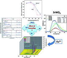
SrWO4 (SWO) and Eu3+ doped SrWO4 (SEWO) scheelite samples were synthesized using a polyol method. Crystallite sizes of the as prepared samples annealed at 300 and 500 °C are in a similar range (<20 nm) whereas those annealed at 700 and 900 °C are about ∼40–50 nm and 80–100 nm, respectively. Photoluminescence (PL) spectra of SWO samples show a broad peak corresponding to the oxygen to tungsten charge transfer transition. Along with the enhancement in emission intensity in the samples annealed at 700 and 900 °C, there is a blue shift in peak maxima. Our first principles quantum mechanical calculations showed that the break in symmetry of the unit cell of SrWO4 creates inherent defects in the lattice which are responsible for the reduction of the electronic band gap in the SrWO4 sample with decrease in size. On europium doping; energy transfer from the O2− → W6+ charge transfer band to Eu3+ takes place and the reason behind this is explained using density functional theory (DFT) calculations. Based on time resolved PL measurements, it is suggested that Eu3+ ions occupy two sites in SWO; a regular symmetric Sr2+ site and an asymmetric site (closer to charge compensating defects). With increase in annealing temperature, emission intensity as well as asymmetry around europium increased. The changes in asymmetry around europium and defect densities as determined from positron annihilation lifetime spectroscopy (PALS) suggest that though the overall vacancy concentration is reduced with an increase in annealing temperature, it is likely that vacancies closer to europium are slowly annealed out than the others.
Among divalent tungstates, strontium tungstate scores over others because of its unique scintillation properties even at low temperatures and ability to act as a host wherein both laser as well as Raman properties can be exploited together.6 It also has other important applications as optical sensor,6 scintillator,7 laser host8 etc. SrWO4 belongs to scheelite family having tetragonal structure with space group I41/a and point group symmetry C4h6. In SrWO4; Sr2+ and W6+ ion are surrounded by eight and four oxygen atom in the form of dodecahedra and tetrahedra respectively. The site symmetry of Sr2+, W6+ and O2− ion is S4, Td and C1 respectively.9 SrWO4 is known to show self activating luminescence in bluish-green region which is attributed to charge transfer transition10 from oxygen to tungsten (O → W). Not only it is a self activated phosphor, it is found to be an excellent luminescence host owing to its unique crystal structure, high chemical stability, low synthesis temperature etc.11,12
In the last 10 years nanomaterials with optimum size and desired morphology have gained considerable attention owing to their excellent optical, bio-medical, electronic, catalytic properties. In this context; research pertaining to nanoscale luminescent materials is part of the growing advances in nanotechnology. Nano domain leads to both blue and red shift in absorption spectra for metal nanoparticles whereas in semiconductor nanoparticles it is mostly blue shift.13 These differences arise because of quantum confinement effect, generation of additional impurity levels and surface related defects. Meltzer and group14 have reported increased luminescence efficiency in nanocrystalline phase compared to its bulk counterpart which also alters the radiative lifetime.
Because of special spectroscopic characteristics and luminescence dynamics of 4f-electrons, doping of luminescent lanthanide ions in nano-hosts have been demonstrated as an excellent approach to develop highly efficient and stable nanophosphors for future applications. Because of the small grain size, nanophosphors doped with lanthanide ions also exhibit optical properties that differ from its bulk form.
We have chosen Eu3+ as a dopant because of its symmetry sensitive luminescence.15,16 Eu3+ doped tungstate can be an interesting luminescence material because of the possibility of energy transfer from tungstate ion to localized state of europium which results in red phosphor with higher quantum efficiency.
There are quite a few reports on photoluminescence properties of pure7,10,17–24 and europium doped10,25–30 sample. But none of these works systematically explain the effect of annealing temperature on optical properties of pure and europium doped SrWO4. We have tried to correlate the changes in photoluminescence properties as a function of annealing temperature of various europium doped sample with Judd–Ofelt parameter and other related photo physical parameters.
Photoluminescence phenomenon is reported to be strongly affected by presence of defects in the lattice (cation vacancy, vacancy clusters)31 which normally arise during the synthesis or thermal treatment of the phosphor material. In this context positron annihilation lifetime spectroscopy (PALS) has been used to probe the defects. Although PALS is used extensively for studying nanomaterials where defects are naturally present; it can be a great tool to study trivalent lanthanide based phosphor also wherein defects also arises due to charge imbalance (aliovalent doping) such is in case of Eu3+ doped SrWO4. There are quite a few reports where PALS has been proved to be very useful in understanding the defect chemistry of lanthanide based luminescence materials.32–37 Understanding the evolution of defects in the luminescent materials and their influences on the luminescence materials would be an important step in realisation of high efficient phosphors.
Variation in annealing temperature may leads to change in particle size, crystallinity and coordination geometry around europium ion. This also leads to change in type, size and density of defects. We have used PALS as tool to study the evolution of defects. We have Eu3+ as luminescence probe to study the changes in structural aspect of SrWO4:Eu3+ using time resolved photoluminescence spectroscopy (TRPLS). Based on the defect studies using PALS and luminescence studies involving structural aspects, defect evolution mechanism in these nanophosphors and their influences on luminescence properties is explained.
Photoluminescence measurements were carried out on an Edinburgh supplied CD-920 unit equipped with M-300 monochromators (both at excitation and emission side). The data acquisition and analysis were done using F-900 software provided by Edinburgh Analytical Instruments, UK. Xenon flash lamp (μF2, power-100 watt, Edinburgh make) with frequency range of 10–100 Hz was used as the excitation source. First the excitation spectrum was recorded by fixing λmax in the emission spectrum of Eu(III). The λex was selected so as to obtain the maximum fluorescence output. All the emission spectra were recorded in the wavelength range 350–750 nm with a step of 1.0 nm per second. Emission spectra for a particular sample was recorded with a lamp frequency of 100 Hz. Multiple scans (S/N = 3) were taken to minimize the fluctuations in peak intensity and maximize S/N ratio. Fluorescence lifetime measurements are based on well established time-correlated single-photon counting (TCSPC) technique.
Positron annihilation lifetime spectroscopy (PALS) measurements were carried out using a fast–fast coincidence system with plastic scintillation detectors. The time resolution of the spectrometer was 260 ps. Carrier free 22Na, (15 μCi) deposited and dried between two 8 micron polyimide films (Alfa Aesar) was used as positron source. The positron source was completely immersed in powder samples to stop all positrons in the sample. The same powder sample was annealed at the next higher temperature after each positron lifetime measurements. Approximately 106 counts were recorded in each spectrum. The computer program, PATFIT-88 (ref. 39) was used for the time resolution convoluted multi-exponential decay analysis of the positron lifetime spectra. Silicon was used as reference for correcting for the positron annihilations in the source.
![]() | ||
Fig. 1 Powder XRD pattern of as prepared and annealed samples of (a) pure SrWO4 (SWO) and (b) europium doped SrWO4 (SEWO). |
The cell parameters are as follows; a = 5.391 Å and c = 11.893 Å.46 This compound has scheelite type of structure as shown in ESI [(Fig. S1† ESI#)]. It has eight symmetry elements having body centered tetragonal primitive cell. Each tungsten atom is surrounded by four equivalent oxygens in tetrahedral symmetry and each Sr cation share corners of eight WO4 tetrahedra.47
As the annealing temperature was increased from room temperature to 900 °C, the peak width was seen to decrease. So to determine the full-width at half maximum (FWMH) of the highest intensity peak at 27.66°, the peak was fitted using pseudo Voigt function. The particle size was determined from broadening of XRD reflections by using Scherrer formula;
![]() | (1) |
Sample | FWHM in 2θ scale | Particle size (nm) |
---|---|---|
Pure SrWO4 | ||
SWO-900 | 0.18873 | 106 |
SWO-700 | 0.23507 | 51 |
SWO-500 | 0.48702 | 18 |
SWO-300 | 0.53964 | 16 |
SWO-AP (25 °C) | 0.52779 | 16 |
![]() |
||
Europium doped SrWO4 | ||
SEWO-900 | 0.19975 | 81 |
SEWO-700 | 0.27248 | 39 |
SEWO-500 | 0.48796 | 18 |
SEWO-300 | 0.47831 | 18 |
SEWO-AP (25 °C) | 0.51482 | 17 |
It is seen from the table that as prepared samples have particle size of about 16–17 nm. The nanoparticle size didn't increase much with annealing till the temperature of 500 °C and increased significantly on annealing at higher temperatures.
![]() | ||
Fig. 2 (a) TEM image of SWO-AP nanoparticles and its HRTEM image are shown as inset and (b) its SAED pattern. |
The rings could be indexed to (101), (112), (004), (114), (200), (204), (220), (116) and (312) crystallographic planes and could be successfully indexed to tetragonal phase of SrWO4 which is in agreement with XRD results (JCPDS no. 08-0490). Inset of Fig. 2a shows the high-resolution TEM image where lattice fringes could be observed. The distance of 2.003 Å between the adjacent planes matches well with that of the (204) plane of the tetragonal SrWO4 lattice.
TEM measurements were also carried out on SWO-300, 500, 700 and 900 and their respective micrographs are also shown in Fig. 3a–d. As the annealing temperature is increased to 300 and then to 500 °C; some of the nanosphere cluster together to form larger cylinder type nanorods having length 0.5–1.0 μm and diameter is less than 50 nm. The majority the grains in SWO-300 and 500 are randomly oriented and the particles are agglomerated. As shown in Fig. 3, when the annealing temperature is elevated to 700 and 900 °C, the particles grow and join together to form large clusters which can be easily seen in the inset of Fig. 3d. The agglomerate can be seen in the range of 200–300 nm.
![]() | ||
Fig. 3 TEM image of (a) SWO-300 (b) SWO-500 (c) SWO-700 and SWO-900. Magnified image of agglomerate in SWO-900 is shown as inset in Fig. 4d. |
![]() | ||
Fig. 4 (a) Emission spectra (b) CIE color coordinate diagram of SrWO4 crystallites annealed at different temperature. Inset in Fig. 5a shows the lifetime values of strontium tungstate samples. |
Inset in Fig. 4a shows the average lifetime of SrWO4 samples. It can be seen from Fig. 4 that the emission intensity and PL average lifetimes initially increase with annealing up to 700 °C, after that though lifetime saturates, the emission intensity decreases. Initial rise in lifetime and intensity and then saturation can be attributed to reduction in non-radiative mode of relaxation as a result of decreased defect concentration with increase in annealing temperature. The changes in the average defect density with annealing temperature are supported by the PALS data (Section 3.7).
TEM studies have shown that the 900 °C annealed samples are highly agglomerated and larger sized. The particle agglomeration can lead to reduced emission intensity because of scattering effects on incident and emitted light.
To check colour purity of the various strontium tungstate sample, CIE (Commission Internationale de l'éclairage) colour coordinates have been calculated from their respective corrected emission spectra of Fig. 4a. The calculated CIE indices values are mentioned in Table T2† (ESI#) and are indicated pictorially in CIE index diagram (Fig. 4b). From Fig. 4b it is clear that the emission from the strontium tungstate nanostructure sample (SWO-AP, 300 and 500) corresponds to green region whereas bulk like sample (SWO-700 and 900) show blue emission. So it can be said that strontium tungstate samples show size dependent colour tunability.
![]() | ||
Fig. 5 PAW-PBE calculated electronic density of states (total and angular momentum decomposed) of the SrWO4 scheelite phase. Vertical lines at zero represent Fermi energy. |
In order to simulate order–disorder present in the system as well as structural complex vacancies associated with them structural models were built by displacement of W atom situated at position (0.5, 0.25, 0.375) in direct lattice co-ordinate (as shown in Fig. S2a† ESI#) of ordered SrWO4 (o-SWO). In o-SWO structure all the W–O bond lengths are 1.81 Å in WO4 cluster. In order to generate disordered SrWO4 model (d-SWO), the displacement of one W atom in the unit-cell was moved in such a fashion that one W–O bond length reduces and other three W–O bond lengths increase by same amount in one WO4 cluster. We worked out a formula by which this displacement can be made and is expressed as: x = 1.713345865y; z = 3.31526088y(a/c)2, where x, y, z are atomic position of W atom in the unit cell of d-SW after displacement and a and c are lattice parameters of SrWO4 unit-cell. We varied y value from 0.01 to 0.02 and generated two distortion model represented by d-SWO-d1 and d-SWO-d2 which consider different degree of disorder in the o-SWO system. It is trivial to note that y = 0.0 is o-SWO model. CaWO4 and CaMoO4 are also having similar structure as SrWO4. Marques et al.51 and Campos et al.52 used similar distortion model to introduce disorderness in the [WO4]/[MoO4] clusters. In our study we used two different degree of distortion in [WO4] cluster represented by d-SWO-d1 and d-SWO-d2.
The W atom displacement and W–O bond lengths in the different distortion models considered are summarized in Table 2. Displacement of W atom breaks the bonds and W atoms are surrounded by three oxygen atoms in its first coordination sphere of distorted WO4 cluster. These three models can describe the continuous behavior of the order in o-SWO and introduce disordered discontinuities in disordered d-SWO; each of the [WO4] complex clusters is accompanied by a distortion that leads to [WO3. VOZ], where .51 Fig. 6 shows total and angular momentum decomposed DOS of d-SWO-d1 and d-SWO-d2 distortion model. Overall bonding characteristics of d-SWO-d1 model is very similar to o-SWO but contribution of the O 2p states just below the Fermi energy and W 5d states at the bottom of conduction band are higher compared to o-SWO model. Moreover, the electronic band-gap of d-SWO-d1 model (3.7 eV) is smaller compared to o-SWO model. Bonding characteristics of d-SWO-d2 distortion model is different from o-SWO and d-SWO-d1 distortion model. The overall covalent bonding features have reduced due to reduction of pseudo-gap in the valence band of d-SWO-d2 distortion model. The contribution of W 5d states and O 2p states at bottom of the conduction band has increased and as a result overall band-gap has decreased to 3.2 eV.
Distortion model | W atom displacement amount | W–O1 bond length | W–O2 bond length | DFT calculated band-gap (Eg) eV |
---|---|---|---|---|
o-SWO | y = 0.00 | 1.81 | 1.81 | 4.00 |
d-SWO-d1 | y = 0.01 | 1.67 | 1.86 | 3.7 |
d-SWO-d2 | y = 0.02 | 1.53 | 1.92 | 3.2 |
![]() | ||
Fig. 6 PAW-PBE calculated electronic density of states (total and angular momentum decomposed) of the d-SWO-d1 (a) and d-SWO-d2 (b) structural model. Vertical lines at zero represent Fermi energy. |
PL emission spectra (Fig. 4a) of SWO samples at room temperature is typical of a multiphonon process, i.e., a system in which relaxation occurs by several paths, involving the participation of numerous states within the band gap of the material. This behavior is associated with the structural disorder of SWO and indicates the presence of additional electronic levels in the forbidden band gap of the material. With increase of annealing temperature, the peak of the PL spectrum shifts towards lower wavelengths indicating increase of optical band-gap by reduction of inherent structural defects present in SWO. Our first principles quantum mechanical calculations have already shown that the break in symmetry creates inherent defects in the lattice and is responsible for the presence of electronic states in the band gap. Therefore, our distortion model qualitatively explains the red shift in the emission spectra of SrWO4 nanoparticles.
![]() | ||
Fig. 7 Excitation spectra of SrWO4:Eu samples annealed at various temperature. Inset shows the resolved component of charge transfer transition due O–Eu and O–W. |
Upon excitation with 395 nm (Fig. S3,† ESI#), corresponding to the 7F0 → 5L6 excitation band of Eu3+, emission features similar to that of CTB excitation were observed but with substantially reduced intensity. It is known that the intensities of emission band on excitation with 395 nm are quite low compared to that ligand to metal charge transfer (LMCT) because of forbidden character of f–f transition.
Fig. 8 shows the emission spectra of Eu3+ doped SrWO4 (SEWO) samples at various annealing temperature under excitation wavelength of 254 nm. It was observed that, relative emission intensity of europium doped sample follows exactly the same trend as was observed for the undoped sample i.e. emission intensity increases with increase in temperature up to 700 °C and after that it reduces. This enhancement up to 700 °C can be attributed to decrease in non-radiative transitions probability as a result of annealing defects with increasing annealing temperature. Beyond 700 °C particles agglomerate to such extent that it causes scattering of the emitted light and thereby decreasing the observed emission intensity. It can be seen from the spectra that for all the samples spectral features remains same; consisting of typical europium emission lines corresponding to 5D0 → 7FJ (J = 1, 2, 3 and 4). Host emission in all the samples decreases substantially indicating significant energy transfer from tungstate to europium ion. It is an interesting to understand why in some cases host–dopant energy transfer takes place and not in others. Host–dopant energy transfer is an important dynamical process because it has become an efficient route to enhance the photoluminescence intensity of dopant ion. This we have explained qualitatively in next section using DFT calculation in europium doped strontium tungstate sample.
Eu3+ emission characteristics are highly sensitive to its local environment because of presence of pure magnetic dipole 5D0–7F1 (ΔJ = ±1) transition and hypersensitive electric dipole 5D0–7F2 transition (ΔJ = ±2). As a result, in the cases where inversion symmetry is present the electric dipole transition (EDT) is strictly forbidden and the magnetic dipole transition (MDT) is usually the most intense emission peak whereas in a site without inversion symmetry EDT is usually the strongest emission line. Because of this peculiarity, europium is used as an intrinsic structural probe to map changes in local environment and symmetry for different kinds of inorganic materials.15,16,53–57
From the respective emission spectra of SEWO samples; it can be seen that in all the cases electric dipole 5D0–7F2 transition (EDT, ΔJ = ±2) is stronger than magnetic dipole transition (MDT) which is indicative of low symmetry around europium ion. Due to different ionic charge and the large difference in the ionic size between W6+ (42 pm) and Eu3+ (107 pm), Eu3+ is expected to occupy the Sr2+ (113 pm) site in SEWO which is justifiable because the electronic densities of Eu3+ and Sr2+ at their coordination numbers are analogous.58 But still symmetry is low because of valence mismatch between Eu3+ and Sr2+ ion which necessitates the presence of charge compensating defects.
In addition to the intrinsic defects like surface defects, oxygen vacancies that can be present even in the undoped sample, strontium vacancies are also expected in SEWO samples. It is reflected as higher average positron lifetime in the PALS data discussed in next section.
The more suitable spectroscopic probe is asymmetry ratio which is defined as the ratio of integral intensity of hypersensitive electric dipole 5D0–7F2 transition (ΔJ = ±2) to pure magnetic dipole 5D0–7F1 (ΔJ = ±1) transition and symbolised by R/O. The R/O value and integral MDT intensities are mentioned in Table 3.
Sample | Integral area of 5D0–7F1 transition (MDT) | R/O (= IEDT/IMDT) |
---|---|---|
SEWO-AP | 48![]() |
5.22 |
SEWO-300 | 50![]() |
7.01 |
SEWO-500 | 58![]() |
7.34 |
SEWO-700 | 77![]() |
8.53 |
SEWO-900 | 87![]() |
6.21 |
It can be seen from this table that asymmetry ratio increase with increase in temperature up to 700 °C which is an indication of highly asymmetric environment around europium ion and its increase with annealing temperature. But interestingly for SEWO-900; asymmetry ratio is less. This could be due to near complete annealing of the defects as suggested by positron data (Section 3.7). However, increase in symmetry around europium due to segregation of Eu2O3 can't be ruled out though the separate phase is not observed in XRD measurements.
Another interesting observation is that in the case of SEWO-900 extent of energy transfer from O–W charge transfer band (host) to Eu3+ is comparatively less compared to other samples which is easily seen from the relative intense host band (Fig. S4† ESI#) in its respective emission spectrum. Reduction in extent of energy transfer in SEWO-900 supports the possibilities like segregation of europium oxide from SrWO4, formation of different phases such as Eu2(WO4)3 at high temperature by diffusion of europium to the surface.59
![]() | (2) |
This is indication of the fact that europium ions are present at two different sites in SEWO. The lifetime values with their relative percentage are given in Table 4. As discussed earlier, the substitution of Sr2+ with Eu3+ (wherein +2 is replaced by +3) may result in significant lattice distortion and thus descend the original S4 site symmetry around Sr2+ ion to very low symmetry viz. Cn or Cnv. Therefore there are sites other than regular Sr2+ site which Eu3+ can occupy. Let us call regular Sr2+ with symmetric environment as S1 and other site closer to charge compensating defects with reduced symmetry as S2. Assuming a given phonon energy (lanthanide occupying the same host), a relatively longer life time is attributed to a more symmetric site where f–f transition becomes more forbidden. A shorter life time is often associated with an asymmetric site due to relaxation in the selection rules. In SWO scheelite structure, Eu3+ ions occupy two sites; regular symmetric Sr2+ site (S1) and asymmetric site S2 which will be closer to charge compensating defects. Short lived species X1 arises because of Eu3+ ions occupying S2 site without inversion symmetry, whereas long-lived species X2 can be ascribed to Eu3+ ions occupying S1 site with inversion symmetry. Such site selective spectroscopy of Eu3+ in Sr2SiO4 and SrZrO3 is reported by our group.60,61
Samples | Short lived species, X1 (in μs) | Long lived species, X2 (in ms) |
---|---|---|
SEWO-AP | 410.63 (33%) | 1.16 (67%) |
SEWO-300 | 471.11 (36%) | 1.21 (64%) |
SEWO-500 | 492.49 (29%) | 1.42 (71%) |
SEWO-700 | 532.52 (27%) | 1.36 (73%) |
SEWO-900 | 771.23 (91%) | 1.859 (9%) |
It can also be seen from the Table 4 that luminescence lifetime values for both X1 and X2 species increase with increase in annealing temperature and is again attributed to reduction in non-radiative pathways. But the interesting observation from Table 4 is that for the sample annealed up to 700 °C percentage of short lived species (X1) is relatively less compared to long lived one (X2). But for 900 °C annealed sample; situation reverses and percentage of X1 species is larger than X2.
In order to identify the environment associated with the species exhibiting different life-times, time resolved emission spectra (TRES) were recorded at different time-delays with constant integration time. Spectra for long lived (X2) and short lived (X1) species obtained after mathematical calculations (Table T3† ESI#) were distinctly different (Fig. S6† ESI#). For X2; magnetic dipole transition corresponding to 5D0 → 7F1 line is much intense than electric dipole transition whereas for X1 reverse is true i.e. electric dipole 5D0 → 7F2 transition at 615 is intense than MDT. This is in correspondence with phonon energy concept, where long lived species (X2) will have more symmetric component than short lived species.
Judd–Ofelt analysis is a very powerful tool for evaluating photo physical properties of europium ion in doped sample using the corrected emission spectrum. The details of all the calculations used are explained extensively elsewhere.53,55 It is well known that the Judd–Ofelt parameter Ω2, gives information about the covalent character and structural changes in the local vicinity around Eu3+ ion (short range effects), whereas Ω4 gives information about bulk properties such as viscosity and rigidity of the inorganic matrices (long range effects). Higher the value of Ω2; more is the covalency of M–O bond and more polarizable environments around metal ion. Judd–Ofelt parameter and other photo physical properties of Eu3+ doped SrWO4 samples are listed Table 5. It can be very well seen from the Table 5 SEWO-700 samples is best in terms of luminescence output with highest radiative transition rate and quantum efficiency. This is in sync with our emission and lifetime spectroscopy data. On the other hand SEWO-900 sample is having least quantum efficiency and highest probability for non-radiative transition. This might be because of particle agglomeration or phase separation of europium. It can be seen from the Table 5 that Ω2 value is maximum for SEWO-700 and minimum for SEWO-AP. This is also reflected in asymmetry (O/R) ratio values. This is an indication that the extent of asymmetric environment around europium ion is maximum in case of SEWO-700 and minimum in SEWO-AP. But beyond 700 °C the value of Ω2 decreases which is an indication of decreased polarizability around Eu3+ ion in SEWO-900. This can be explained on the basis of enhanced symmetry around Eu3+ at 900 °C as a result of increased crystallinity which is also seen from the intense magnetic dipole transition in case of SEWO-900. Moreover trend in J–O parameter for all the SEWO samples shows that Ω2 > Ω4; which is related to high asymmetry of the Eu3+ surrounding environment in all SEWO samples. The spectral features obtained for all samples are almost similar and can be attributed to Eu3+ ions in asymmetric environment without inversion symmetry. The difference in τexp and τR can be attributed to decay by nonradiative pathways.
Sample | τav (μs) | ARAD (s−1) | ANRAD (s−1) | η (%) | Ω2 (× 10−20 cm2) | Ω4 (× 10−20 cm2) |
---|---|---|---|---|---|---|
SEWO-AP | 947 | 441 | 602 | 39.2 | 4.34 | 3.53 |
SEWO-300 | 956 | 457 | 588 | 43.7 | 5.25 | 3.64 |
SEWO-500 | 983 | 581 | 469 | 57.1 | 7.00 | 4.41 |
SEWO-700 | 1140 | 668 | 382 | 76.1 | 8.43 | 4.55 |
SEWO-900 | 873 | 421 | 629 | 36.7 | 6.18 | 0.396 |
The shortest component (τ1p) is usually attributed to free positron annihilation in the defect free bulk. However, the nanoparticles are seldom free from defects and the τ1p is usually much longer than expected in defect free material.62,63 The τ1p in nano materials arises due to smaller vacancies (like mono vacancies or divacancies). In the present case, in undoped samples (SWO), the τ1p is about 307 ps in SWO-AP and it monotonically reduced to ∼218 ps upon annealing. The reduction in positron lifetime shows that the defects are annealing out with temperature treatment. The variation in the lifetime is much drastic for the samples annealed at 700 °C and 900 °C. From the XRD data it is seen that the nanoparticle size also drastically increases in the samples annealed at these temperatures. This suggests that these vacancies are getting annealed upon annealing and nanoparticle growth. The trend in the changes in the τ1p in Eu doped samples is almost same as the undoped samples and traces size of the nanoparticles.
The second lifetime component (τ2p) in these materials/nanoparticles arises due larger vacancy clusters. The average electron density in larger size voids is much smaller and hence the lifetimes are much longer than τ1p. The positrons can diffuse to the surface of the nanoparticles where there can be large boundary like defects. The τ2p values in both undoped and Eu-doped samples are much larger than τ1 suggesting that these are from larger defect clusters or imperfections. The value of τ2p in SWO-AP is ∼580 ps while it is 615 ps in Eu-doped sample, both much longer than τ1p of 310 ps. It has been shown that the surface modification of nanoparticles only changes τ2p without much change in τ1p while changing the oxygen vacancy concentrations in TiO2 nanoparticles changes τ1p.64,65 Based on these studies it has been suggested that the τ1p corresponds to smaller vacancies mainly present in the bulk of the nanoparticles while τ2p arises due to larger surface defects on the nanoparticles.66,67 The value of τ2p in both undoped and Eu-doped SrWO4 samples reduced upon annealing at higher temperatures. The reduction in τ2p indicates that as the size of the nanoparticle increasing, not only the surface area is reduced; the imperfections associated with the surface of the nanoparticles are also reduced.
The fraction of positrons annihilating with lifetimes of τ1p and τ1p (I1p & I2p) is the measure of positrons trapped in smaller vacancies and larger voids respectively. Unlike the positron lifetimes (τ1p and τ2p), the positron intensities show non-monotonic behaviour with annealing temperature. Partially the reason for this lies in the fact that the positron intensities obtained after normalizing the total positron intensities to 100% and hence, the changes in the intensities corresponding to positron annihilation from different states are not completely independent. It is seen from the Fig. 10a and b that I1p and I2p show trends opposite to each other (I3p decreasing though the extent of change is much less). In the SrWO4 samples, I1p decreases due to annealing up to 500 °C and then increases. As discussed earlier, the nanoparticle size in the samples annealed at temperatures of 700 °C and 900 °C is larger. The initial decrease in the I1p is due to annealing out of the smaller vacancies present in the nanoparticles. At higher temperature annealing, though the intensity I1p has increased again, the positron lifetimes (τ1p) values are in the range of 210 ps already suggesting the positron component is due positron annihilations in the bulk. The large intensity corresponding to this lifetime suggests that smaller defects are annealed out while the presence of τ2p shows that some defects are still present in the surface regions of the nanoparticles. However, it may be noted that τ2p values in the samples annealed at 900 °C are much lower than as prepared samples. In the Eu-doped SrWO4, the I1p showed continuous decrease with increase in annealing temperature and the decrease is more drastic at higher temperature annealing. Correspondingly I2p shows increase in samples annealed at higher temperature. The results suggest the larger voids have not completely annealed out Eu-doped samples as yet and it is likely that the smaller defects have migrated to the surface However, the τ2p values in the samples annealed at 900 °C have reached to values that only above the τ2 values in the as prepared samples.
The long lived o-Ps lifetime (τ3p in the range of 2 to 2.5 ns) component in these powder samples arises due to the positron annihilation at the intergranular spaces.68,69 In all the samples, the intensity of this component decreases with increase in the nanoparticles size though overall variation (4.5 to 2.0%) is small. The o-Ps lifetime also shows decrease with increase in the particle size except in the as prepared samples. The lower lifetime in the as prepared samples might be due to the presence of hydroxyl groups on the surface of the particles as they are prepared in polyol method. The hydroxyl functional groups are removed in high temperature annealing.
In the cases where τ1p and τ2p values are close by, the mean lifetimes (τm) are compared. In the present case, the mean lifetimes in all the samples are calculated as:
In calculating the mean lifetime of the positron, τ3p values (o-Ps lifetimes) are not considered. They are expected to be from the grain boundaries in the powder samples. Whenever there is o-Ps component in the positron lifetime spectrum, there should be corresponding p-Ps component of 125 ps lifetime. In the present case, the o-Ps intensity is in the range of 4 to 2% and hence p-Ps component would be in the range of ∼1 to 0.5%. It could not be resolved into separate component with respect τ1p which is more than 80%. However, the variations in the τ1p or the mean lifetime calculated due to exclusion of p-Ps are expected to be minimal.
The mean lifetimes of the samples is shown in Fig. 11. The mean positron lifetime traces the profile of average electron density or defect density in the samples. It is seen from the Fig. 11 that the average positron lifetime decreases with increase in annealing temperature. The reduction is drastic for the samples annealed at 700 or 900 °C. This shows that defects are reduced as the particle size is increased. The photoluminescence intensities increased with decrease in the defect density as the non-radiative fraction is reduced. The lower emission intensity in 900 °C has been attributed to particle agglomeration rather than the defects. The mean lifetimes in the SrWO4 are marginally lower than Eu-doped samples. This is on expected lines as Eu3+ substitution in place of Sr2+ would add to the cation vacancies in the sample. The near equal mean lifetimes in the as-prepared SrWO4 to the Eu-doped sample indicates the large number of intrinsic defects at such smaller size of nanoparticles.
![]() | ||
Fig. 11 Mean positron lifetimes in undoped and Eu-doped SrWO4 annealed at different temperatures for 2 hours in air. |
The increase in the photoluminescence lifetimes with annealing suggest the decrease in the defect concentrations, which is also supported by the positron lifetime data. The changes in asymmetry around europium suggest that though overall vacancy concentration is reduced with increase in annealing temperature, it is likely that besides the overall reduction in the vacancy concentration, the vacancies are also migrated closer to europium. The reduction in the vacancy concentration would enhance the photoluminescence intensity and photoluminescence lifetimes; the vacancy migration would result in enhanced asymmetry around europium.
On europium doping, energy is transferred from host to dopant ion. Coincidence of Eu f-states with impurity states at the bottom of the conduction band as shown by DFT calculations clearly suggests that the photo-excited electrons in the valence band may migrate to the Eu-related impurity energy levels through the process of energy transfer. It was observed that with increase in annealing temperature up to 700 °C emission intensity, lifetime and asymmetry ratio increase which is in sync with positron lifetime data. At 900 °C it's possible that europium is migrated to surface and forms a separates phase which is depicted in reduced host–dopant energy transfer, almost predominate slow lifetime and increased symmetry. The increase in the photoluminescence lifetimes with annealing suggest the decrease in the defect concentrations, which is also supported by the positron lifetime data. The changes in asymmetry around europium suggest that though overall vacancy concentration is reduced with increase in annealing temperature, it is likely that vacancies closer to europium are slowly annealed out than the others. Photo physical property reveals the size tunable emission of SWO and high quantum efficiency of SEWO-700. SEWO-700 can be a potential candidate for red emitting phosphor in future white LEDs.
Footnote |
† Electronic supplementary information (ESI) available. See DOI: 10.1039/c5ra23876e |
This journal is © The Royal Society of Chemistry 2016 |