
Hierarchical growth of ZnO nanorods over SnO2 seed layer: insights into electronic properties from photocatalytic activity†
Luís F. Da Silva*a,
Osmando F. Lopesb,
Ariadne C. Cattoc,
Waldir Avansi Jr.d,
Maria I. B. Bernardic,
Máximo Siu Lic,
Caue Ribeiro b and
Elson Longoa
b and
Elson Longoa
aLIEC, Instituto de Química, Universidade Estadual Paulista, P.O. Box 355, 14800-900 Araraquara, SP, Brazil. E-mail: lfsilva83@gmail.com
bEMBRAPA Instrumentação, Rua XV de novembro, 1452, 13560-970 São Carlos, SP, Brazil
cInstituto de Física de São Carlos, Universidade de São Paulo, Avenida Trabalhador São-carlense, 400, 13566-590 São Carlos, SP, Brazil
dDepartamento de Física, Universidade Federal de São Carlos, Rodovia Washington Luiz, km 235, 13565-905 São Carlos, SP, Brazil
First published on 22nd December 2015
Abstract
The use of nanostructured heterojunctions has been a promising option for hindering the charge recombination and thus enhancing the photocatalytic performance of catalysts. Here we present a simple strategy to hierarchically grow heterostructures using a hydrothermal treatment route. A buffer SnO2 film was produced by a sol–gel derived method, resulting in a film of approximately 100 nm composed of 5–10 nm nanoparticles. X-ray diffraction and scanning electron microscopy revealed preferential growth of the nanorod-like structures along the c-axis perpendicular to the SnO2 film, with an average nanorod diameter and length of approximately 160 nm and 1.5 μm, respectively. The photoluminescence spectra of ZnO–SnO2 revealed a reduction in UV emission compared to individual ZnO nanorods, indicating that the recombination of the photogenerated carriers was inhibited in the heterojunction. This behavior was confirmed by evaluating the photocatalytic performance of such films against methylene blue degradation, showing that the as-prepared ZnO–SnO2 heterojunction was superior to the individual semiconductors, ZnO and SnO2.
1. Introduction
Metal oxide semiconductors (MOS) have attracted considerable interest from many researchers due to their unique properties that allow numerous technological applications such as in gas sensor devices,1–3 dye-sensitized solar cells,4–6 and photocatalysis.7–12 In past decades, photocatalysis technology has attracted considerable interest for solving environmental problems, especially for the removal of contaminants in water and air.7,8,13Despite the potential application of MOS to the photodegradation of non-biodegradable pollutants, the high electron–hole (e−/h+) recombination rates impair the photocatalytic reaction efficiency.14–17 Therefore, great efforts have been made to further improve the performance of MOS, for example, the coupling or creation of junctions between semiconductors (homo and/or heterojunctions) has been a promising option for hindering the charge recombination and thus enhancing the photocatalytic performance. Indeed, several articles have demonstrated the great technological potential of the different heterostructured compounds, for example, Fe3O4–WO3,18 TiO2–V2O5,19 TiO2–SnO2,20 TiO2–WO3,21 ZnO–CuO,22 and ZnO–SnO2.13,15,23–25
ZnO and SnO2 are important n-type semiconductors (Egap = 3.37 eV and 3.6 eV, respectively at 300 K) that have attracted considerable interest in diverse applications.3,26–29 The literature has reported that the junction of these semiconductors, forming a suitable type-II heterostructure, can further enhance their properties mainly due to the efficient charge separation.13,23,25,30
Recently, Park and co-workers synthesized SnO2-core/ZnO-shell nanowires through a two-step process consisting of a thermal evaporation followed by an atomic layer deposition.25 A remarkably improvement of the UV-activated gas-sensing properties towards different NO2 gas concentrations was reported.25 Additionally, using a two-step procedure and through thermal evaporation, Huang and co-workers decorated ZnO nanorods with SnO2 nanoparticles obtaining an improvement in photocatalytic activity for rhodamine B oxidation in comparison to pure ZnO nanorods, which was attributed to heterojunction formation.23
Thus far, the majority of the photocatalysis applied for the removal of contaminants in water have been in powder form. However, the difficulties in the recovery and reuse of these photocatalysts has discouraged their application in water purification systems.31,32 For this reason, the use of photocatalysts based on thick and/or thin film forms has been encouraged.31,33–36
Physical and/or chemical methods have been employed for the synthesis of various heterostructures.6,13,14,23,25,37 Among these methods, the hydrothermal approach can be considered a simple and versatile methodology to obtain various compounds in the forms of ceramic powders and/or films.3,10,38–41 Its main advantages include simple manipulation, low energy consumption, good reproducibility, and easy control and/or design of microstructural properties.3,11,41,42
We report here on the crystal engineering processes for obtaining ZnO–SnO2 heterojunctions via hydrothermal method, while studying the relationship between their morphological and photocatalytic properties. X-ray diffraction, scanning electron microscopy, and high-resolution transmission electron microscopy were applied to investigate the formation of the ZnO rod-like structures over a SnO2 thin film. To gain information about the surface and electronic properties, photoluminescence and X-ray photoelectron spectroscopy were also performed, respectively. The photocatalytic activity was monitored using methylene blue (MB) dye under UV light activation.
2. Experimental section
2.1. Preparation of ZnO–SnO2 heterojunction
The growth of ZnO nanorod-like structures on SnO2 nanoparticles was accomplished using the hydrothermal treatment method. The preparation process of the hierarchical ZnO rod-like structures is detailed below. To grow ZnO rod-like structures on a nanostructured SnO2 thin film, zinc nitrate [Zn(NO3)2·6H2O, Aldrich, >99%] and hexamethylenetetramine (C6H12N4, HMTA, Aldrich, >99%) were dissolved in deionized water under vigorous stirring at room temperature. Then, the SnO2 seed layer was immersed in the solution with the SnO2 layer (i.e., thin film) facing down. The details of the synthesis and the deposition procedure of nanostructured SnO2 thin films may be found in the ESI.† The ZnO nanorods were hydrothermally grown by holding the screw-capped bottle in a furnace for 4 hours at 110 °C with a heating rate of 10 °C min−1. At the end of the hydrothermal treatment, the samples were removed from the solution, thoroughly washed several times with deionized water and isopropyl alcohol to remove loosely adherent white powder that had precipitated during the deposition, and dried overnight at 80 °C. To compare the photoluminescent and photocatalytic properties, we also prepared ZnO nanorods over a ZnO thin film (labeled as ZnO–ZnO) following the procedure described in ref. 3.2.2. Materials characterization
XRD patterns were determined using a Rigaku diffractometer (model ULTIMA IV) operating in Bragg configuration using a CuKα radiation source. The data were collected in the 2θ = 20–60° range, with a 0.02° step at a 2° min−1 scanning speed. The morphological properties of the SnO2 (seed layer) and ZnO–SnO2 films were analyzed using a field emission scanning electron microscope (FESEM, Zeiss Supra35 and JEOL JSM-6701F) operating at 10 kV. The average nanorod size was estimated by measuring 150 particles from the FESEM micrographs. The samples were also studied by the SEM analysis of the as-prepared films perpendicular to the c-axis of the ZnO nanorods. Transmission electron microscopy (TEM) was performed using a JEOL JEM 2100F operating at 200 kV. The sample was prepared for TEM analysis using a scraping method in which the ZnO nanorods were removed from the SnO2 layer, dispersed, and dropped on a copper grid covered with a thin layer of carbon. Photoluminescence spectra were collected using a Thermal Jarrel-Ash Monospec 27 monochromator and a Hamamatsu R446 photomultiplier linked with a data acquisition system consisting of a SR-530 lock-in controlled by microcomputer. The samples were excited by 325 nm wavelength light from a krypton ion laser (Coherent Innova) and the nominal output power of the laser was kept at 200 mW. The monochromator slit width used was 200 μm. All measurements were collected at room temperature. X-ray photoelectron spectroscopy (XPS) was performed on a Thermo Scientific K-Alpha spectrometer using a monochromatic Al Kα X-ray source. The spectra were peak fitted using the Casa XPS software, and all binding energies were given with reference to the C 1s signal (284.9 eV) arising from the surface hydrocarbons.2.3. Photocatalytic activity experiments
The catalytic performance of the photocatalysts was probed by methylene blue (MB) dye oxidation under UV light. Rectangular samples of SnO2, ZnO–ZnO, and ZnO–SnO2 (area = 57.72(5) mm2) films were immersed in 10 mL of an aqueous MB dye solution, 10 mg L−1. Atomic force microscopy (AFM, Veeco, NanoScope V, tapping mode) was performed to determine the Rrms (root-mean-square) roughness of the samples, and the values obtained were 3.5 nm (SnO2), 350.0 nm (ZnO–ZnO), and 230.0 nm (ZnO–SnO2). AFM images of the photocatalyst samples are shown in Fig. S1.† The solution containing the photocatalysts as rectangular films was placed in a photo-reactor at controlled temperature (20 °C) and illuminated by six UV lamps (TUV Philips, 15 W, and maximum intensity at 254 nm) with an optical irradiance of approximately 35 mW cm−2. The color removal of the MB dye solutions was monitored by its absorption maximum at 665 nm using an UV-VIS spectrophotometer (Shimadzu-UV-1601 PC spectrophotometer) at different times of light exposure. To test the direct UV-photolysis of the dye, blank experiments were performed using a MB dye solution without any catalyst. Before the experiments, the suspensions were left in darkness for 30 min to establish the adsorption–desorption equilibrium of the dyes on the catalyst surface. However, it was observed that color removal through the adsorption process could be neglected.3. Results and discussion
Fig. 1 shows the X-ray diffraction (XRD) patterns of a nanostructured SnO2 thin film and the ZnO nanorods grown on the SnO2 seed layer (Fig. 1a). All diffraction peaks were indexed as a hexagonal wurtzite structure of ZnO with the P63mc space group and silicon, according to Joint Committee on Powder Diffraction Standards (JCPDS) file 36-1451. The broader peaks were attributed to a tetragonal SnO2 phase (JCPDS file 41-1445). No additional peaks related to undesirable phases were observed. Furthermore, it can be observed that the intensity of the (002) peak is higher than the other peaks, suggesting a preferential orientation of the nanorods along the c-axis.3 | ||
| Fig. 1 ZnO nanorods grown on a SnO2 thin film (ZnO–SnO2) at 110 °C via the hydrothermal treatment method. (a) X-ray diffraction patterns of ZnO–SnO2 and SnO2 thin films used as seed layers (inset shows a detail region of its pattern). (b) FESEM micrographs of a ZnO–SnO2 sample. | ||
FESEM images of hierarchical ZnO nanorod arrays on a SnO2 thin film are illustrated in Fig. 1b. These images confirmed the preferential crystal growth along the [001] direction and revealed a high density of arrays of hexagonal ZnO rods over the nanostructured SnO2 layer. The average diameter and length of the rods were approximately 160 nm and 1.5 μm, respectively.
In past years, the growth process of hierarchical ZnO rod-like structures via hydrothermal treatment method has been extensively studied.27,43–48 Feng and co-workers reported that the crystal growth process of these arrays of oriented rod-like structures is based on the dissolution-crystallization of ZnO crystalline grains.44 Additionally, the presence of a nucleation seed is essential for the growth process of these nanorods.47–49 In this way, the crystal growth process of the nanorods consists of the nucleation and crystallization of ZnO crystals, followed by their preferential growth along the c-axis, induced by the seed layer,44 as seen in Fig. 1.
Fig. 2 shows cross-sectional FESEM images of the hierarchical ZnO rod-like structures grown on a SnO2 thin film. It is important to note that the FESEM images show that the ZnO nanorods are not vertically well aligned, unlikely grown over a ZnO seed layer (Fig. S2a†) and extensively investigated in the literature.27,43 This fact is likely related to the different surface energy of the SnO2 layer, which affects the formation of the nucleation sites and consequently the crystal growth of the ZnO nanorods. When the hydrothermal treatment was performed over a silicon substrate without a seed layer, the arrays of oriented nanorods were not formed (Fig. S2b†) due to the absence of nucleation sites.49
 | ||
| Fig. 2 FESEM analyses of a ZnO–SnO2 sample. (a–d) Cross-sectional images of the hierarchical ZnO nanorods grown on a SnO2 thin film. | ||
Fig. 2b displays an expanded image from region A (depicted in Fig. 2a) that confirms the presence of the SnO2 thin film with a thickness of approximately 100 nm. Fig. 2c and d show an individual ZnO rod, and it is possible to observe the presence of SnO2 nanoparticles recovered at its base. This result confirms the formation of ZnO nanorods from the SnO2 seed layer, showing the characteristics of the interface between the materials, which are very important because such characteristics of nanostructure interfaces are considered a challenge in the development of new and efficient heterostructures.17,50 Scheme 1 illustrates of the ZnO nanorod crystal growth over different seed layers via the hydrothermal method.
 | ||
| Scheme 1 Schematic illustration of the crystal growth process of the ZnO nanorods on different seed layers: ZnO (ZnO–ZnO), and SnO2 (ZnO–SnO2). | ||
Similarly, the TEM images confirm the presence of nanoparticles at the base of ZnO nanorods, as shown in Fig. 3a. Indeed, HRTEM and the Fast Fourier Transform (FFT) of individual ZnO nanorods (Fig. 3b and c, respectively) clearly indicate a single crystalline nature of the as-synthesized ZnO nanorods, with preferential growth along the [001] direction. HRTEM and the corresponding FFT were also performed for the SnO2 nanoparticles observed on ZnO nanorods (Fig. 3d and e, respectively). The FFT image corresponding to nanoparticles observed in Fig. 3d could be indexed to a tetragonal SnO2 crystalline phase, which is in good agreement with the XRD results.
 | ||
| Fig. 3 TEM images of single ZnO–SnO2 sample: (a) bright-field TEM image of a single ZnO nanorod containing SnO2 nanoparticles; (b) HRTEM images of a single ZnO nanorod; (c) FFT image corresponding to image illustrated in (b); (d) HRTEM images of SnO2 nanoparticles attached to ZnO nanorods; (e) FFT image corresponding to image illustrated in (c). | ||
The surface structure of the ZnO nanorods grown over the SnO2 film was investigated by XPS, and the experimental results are shown in Fig. 4. The analysis of the surveyed XPS spectrum (Fig. 4a) indicated the presence of the elements C, Zn, and O, where any contamination was observed. The absence of peaks related to Sn in the XPS spectrum can be attributed to the high ZnO nanorod density on the SnO2 thin film. The XPS spectrum of a ZnO–ZnO homojunction is displayed in Fig. S4.†
 | ||
| Fig. 4 XPS spectra of ZnO–SnO2 sample. (a) Survey XPS scan spectrum, (b) Zn 2p, and (c) O 1s core levels. | ||
The high-resolution XPS spectra of Zn 2p, and O 1s are shown in Fig. 4b and c, respectively. The Zn 2p peaks are symmetric and centered at 1021.5 eV and 1044.6 eV, indicating the existence of the Zn2+ state.24,50,51 The O 1s peak was deconvoluted into three Gaussian–Lorentzian curves, as illustrated in Fig. 5c. The lower-energy peak located at 530.1 eV corresponds to O2− ions in Zn–O binding, while the second peak at approximately 531.3 eV is attributed to the oxygen of the surface hydroxyl groups.51,52 The third peak, at 532.1 eV, is due to the chemisorbed oxygen molecule on the ZnO nanorod surface.27,51–53 Additionally, the percentage of hydroxyl groups and chemisorbed oxygen molecules observed in the O 1s spectra was larger in the heterojunction than the homojunction (Fig. 4c and S3†). According to the literature, hydroxyl species present on the semiconductor surfaces could act as active sites, enhancing photocatalysis.8,49,52,54
 | ||
| Fig. 5 Kinetics of the MB dye (10 mg L−1) photodegradation catalyzed by SnO2 thin film, the ZnO–ZnO homojunction, and the ZnO–SnO2 heterojunction under UV light activation. | ||
The photocatalytic performance of the ZnO–SnO2, ZnO–ZnO, and SnO2 samples was evaluated by the degradation of methylene blue (MB) dye under UV light. To obtain kinetic data on the process, it was assumed that the degradation follows a pseudo-first-order reaction.8,55
Fig. 5 shows that all samples were photoactive for MB photodegradation, as the kinetic curves decrease faster than the direct photolysis curve. The observed order of photocatalytic activity related to the studied photocatalysts was ZnO–SnO2 > ZnO–ZnO > SnO2. Remarkably, the ZnO–SnO2 heterojunction led to approximately 30% removal of MB dye after approximately 4 hours of UV illumination, showing the best photocatalytic performance by the heterojunction in contrast to the ZnO–ZnO and SnO2 samples. The pseudo-first-order rate constants for ZnO–SnO2, ZnO–ZnO, and SnO2 were calculated to be 7.7 × 10⁻², 5.3 × 10⁻², and 2.5 × 10⁻² min−1, respectively. Thus, the rate of the reaction catalyzed by the heterojunction was approximately 1.5 times higher than the rate of the reaction catalyzed by ZnO–ZnO sample and 3 times higher than the rate of the reaction catalyzed by the SnO2 seed layer. It is therefore reasonable to believe that the superior photocatalytic performance of the heterojunction (ZnO–SnO2) is due to reduced charge carrier recombination and not solely a surface area effect because the homojunction (ZnO–ZnO) presents a higher surface roughness than the heterojunction, as observed by AFM experiments (Fig. S1†).
Fig. 6 displays the room-temperature photoluminescence (PL) measurements performed on the ZnO–ZnO and ZnO–SnO2 samples. In both spectra, an ultraviolet emission peak was observed at 389 nm, as well as a broad visible emission centered near 600 nm, characteristic of ZnO.56 The UV emission corresponds to a near band-edge (NBE) transition, resulting from the recombination of free excitons of ZnO.23,26,37,53,57 The emission in the visible region can be attributed to single and double ionized oxygen vacancies,26,49,53,57 which have been considered active sites for redox reactions.49
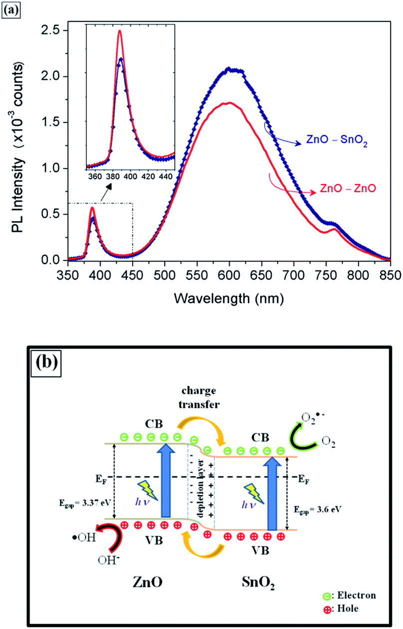 | ||
| Fig. 6 (a) Room-temperature photoluminescence spectra of ZnO nanorods grown on two different seed layers: ZnO and SnO2 thin film. The inset shows an expanded view of the UV region. (b) Schematic illustration of the photocatalytic mechanism of the ZnO–SnO2 heterojunction catalyst. | ||
As seen in Fig. 6a, the PL spectrum of the ZnO–SnO2 heterojunction exhibited a slight reduction in UV emission accompanied by an increase in visible emission compared to the ZnO–ZnO homojunction. The reduction of UV emission suggests that the recombination of the photogenerated electrons and holes was inhibited in the ZnO–SnO2 heterojunction compared with ZnO–ZnO.23,24,37 Additionally, the high visible emission indicates a large number of oxygen defects in the heterojunction, which is in good agreement with the XPS results. Therefore, the good charge carrier separation and the surface oxygen vacancies present in the ZnO–SnO2 heterojunction contribute to its better photocatalytic activity.13,23
The photocatalytic and PL experiments indicated the formation of a type II heterostructure of SnO2 nanoparticles with ZnO nanorods. This scheme, with charge transfer between the semiconductors, is illustrated in Fig. 6b. As can be observed, when the electron–hole pair is photogenerated, the electrons are spontaneously transferred from the CB of ZnO to the CB of SnO2, while the holes are spontaneously transferred from the VB of SnO2 to the VB of ZnO.13,58,59 Therefore, the photogenerated charge carriers are separated in different semiconductors, consequently increasing their lifetime and allowing suitable oxidation and reduction reactions for photocatalytic application.13,58,59
4. Conclusions
This paper reports a simple and versatile way to prepare heterostructured ZnO–SnO2 film for use as a photocatalyst via a hydrothermal treatment method. XRD patterns indicated the presence of crystalline ZnO and SnO2 phases, with a preferential texture along the c-axis of ZnO. An analysis of FESEM and HRTEM images revealed the growth of arrays of rod-like ZnO structures over a SnO2 thin film, forming the ZnO–SnO2 heterojunction. Photocatalytic experiments revealed an improved of performance of the as-prepared ZnO–SnO2 film in the degradation of MB dye under UV light activation. The enhancement of photocatalytic activity was attributed to the good charge separation and the presence of oxygen defects, which were confirmed by PL results. We believe that these findings offer not only a promising strategy to manufacture photocatalysts but also new opportunities for the low-cost preparation of various materials applied in gas sensors and sensitized solar cells.Acknowledgements
The authors are indebted to Prof. Valmor R. Mastelaro for the use of CCMC/USP group installations. We are also grateful for the financial support from the Brazilian research funding institution CNPq (under grant No. 442076/2014-2) and FAPESP (under grants No. 2013/09573-3, 2013/07296-2, 2012/15170-6, and 2013/13888-0). This research was partially conducted at the Brazilian Nanotechnology National Laboratory, LNNano, (Project XPS-18304 and TEM-18566), Campinas, SP, Brazil.Notes and references
- L. F. da Silva, V. R. Mastelaro, A. C. Catto, C. a. Escanhoela, S. Bernardini, S. C. Zílio, E. Longo and K. Aguir, J. Alloys Compd., 2015, 638, 374–379 CrossRef CAS.
- S. Maeng, S.-W. Kim, D.-H. Lee, S.-E. Moon, K.-C. Kim and A. Maiti, ACS Appl. Mater. Interfaces, 2014, 6, 357–363 CAS.
- A. C. Catto, L. F. da Silva, C. Ribeiro, S. Bernardini, K. Aguir, E. Longo and V. R. Mastelaro, RSC Adv., 2015, 5, 19528–19533 RSC.
- B. O'Regan and M. Grätzel, Nature, 1991, 353, 737–740 CrossRef.
- Q. Zhang, T. P. Chou, B. Russo, S. A. Jenekhe and G. Cao, Angew. Chem., Int. Ed., 2008, 47, 2402–2406 CrossRef CAS PubMed.
- N. K. Huu, D.-Y. Son, I.-H. Jang, C.-R. Lee and N.-G. Park, ACS Appl. Mater. Interfaces, 2013, 5, 1038–1043 CAS.
- M. R. Hoffmann, S. T. Martin, W. Choi and D. W. Bahnemann, Chem. Rev., 1995, 95, 69–96 CrossRef CAS.
- O. F. Lopes, E. C. Paris and C. Ribeiro, Appl. Catal., B, 2014, 144, 800–808 CrossRef CAS.
- L. F. da Silva, W. Avansi, J. Andrés, C. Ribeiro, M. L. Moreira, E. Longo and V. R. Mastelaro, Phys. Chem. Chem. Phys., 2013, 15, 12386–12393 RSC.
- W. Avansi, V. R. de Mendonça, O. F. Lopes and C. Ribeiro, RSC Adv., 2015, 5, 12000–12006 RSC.
- Y. Hao, X. Wang and L. Li, Nanoscale, 2014, 6, 7940–7946 RSC.
- A. Fujishima and K. Honda, Nature, 1972, 238, 37–38 CrossRef CAS PubMed.
- M. T. Uddin, Y. Nicolas, C. Olivier, T. Toupance, L. Servant, M. M. Müller, H.-J. Kleebe, J. Ziegler and W. Jaegermann, Inorg. Chem., 2012, 51, 7764–7773 CrossRef CAS PubMed.
- A. Hamrouni, N. Moussa, F. Parrino, A. Di Paola, A. Houas and L. Palmisano, J. Mol. Catal. A: Chem., 2014, 390, 133–141 CrossRef CAS.
- M. Zhang, G. Sheng, J. Fu, T. An, X. Wang and X. Hu, Mater. Lett., 2005, 59, 3641–3644 CrossRef CAS.
- C. Wang, X. Wang, B.-Q. Xu, J. Zhao, B. Mai, P. Peng, G. Sheng and J. Fu, J. Photochem. Photobiol., A, 2004, 168, 47–52 CrossRef CAS.
- R. Marschall, Adv. Funct. Mater., 2014, 24, 2421–2440 CrossRef CAS.
- G. Xi, B. Yue, J. Cao and J. Ye, Chem.–Eur. J., 2011, 17, 5145–5154 CrossRef CAS PubMed.
- M. Epifani, E. Comini, R. Díaz, C. Force, P. Siciliano and G. Faglia, Appl. Surf. Sci., 2015, 351, 1169–1173 CrossRef CAS.
- V. R. de Mendonca, C. J. Dalmaschio, E. R. Leite, M. Niederberger and C. Ribeiro, J. Mater. Chem. A, 2015, 3, 2216–2225 CAS.
- I. A. de Castro, W. Avansi and C. Ribeiro, CrystEngComm, 2014, 16, 1514–1524 RSC.
- Y. Xie, R. Xing, Q. Li, L. Xu and H. Song, Sens. Actuators, B, 2015, 211, 255–262 CrossRef CAS.
- X. Huang, L. Shang, S. Chen, J. Xia, X. Qi, X. Wang, T. Zhang and X.-M. Meng, Nanoscale, 2013, 5, 3828–3833 RSC.
- Z. Zhang, C. Shao, X. Li, L. Zhang, H. Xue, C. Wang and Y. Liu, J. Phys. Chem. C, 2010, 114, 7920–7925 CAS.
- S. Park, S. An, Y. Mun and C. Lee, ACS Appl. Mater. Interfaces, 2013, 5, 4285–4292 CAS.
- M. R. Alenezi, S. J. Henley, N. G. Emerson and S. R. P. Silva, Nanoscale, 2014, 6, 235–247 RSC.
- J. Tang, J. Chai, J. Huang, L. Deng, X. S. Nguyen, L. Sun, T. Venkatesan, Z. Shen, C. B. Tay and S. J. Chua, ACS Appl. Mater. Interfaces, 2015, 7, 4737–4743 CAS.
- M. Guan, X. Zhao, L. Duan, M. Cao, W. Guo, J. Liu and W. Zhang, J. Appl. Phys., 2013, 114, 114302 CrossRef.
- H. Wang and A. L. Rogach, Chem. Mater., 2014, 26, 123–133 CrossRef CAS.
- L. Zheng, Y. Zheng, C. Chen, Y. Zhan, X. Lin, Q. Zheng, K. Wei and J. Zhu, Inorg. Chem., 2009, 48, 1819–1825 CrossRef CAS PubMed.
- C. Sriwong, S. Wongnawa and O. Patarapaiboolchai, J. Environ. Sci., 2012, 24, 464–472 CrossRef CAS.
- C. Ahn, J. Park, D. Kim and S. Jeon, Nanoscale, 2013, 5, 10384–10389 RSC.
- M. Miyauchi, A. Nakajima, T. Watanabe and K. Hashimoto, Chem. Mater., 2002, 14, 2812–2816 CrossRef CAS.
- M. H. Habibi, N. Talebian and J.-H. Choi, Dyes Pigm., 2007, 73, 103–110 CrossRef CAS.
- X. Gu, N. Yu, L. Zhang, J. Yang, J. Hu and Z. Chen, RSC Adv., 2015, 5, 102868–102876 RSC.
- K. T. G. Carvalho, S. C. Fidelis, O. F. Lopes and C. Ribeiro, Ceram. Int., 2015, 41, 10587–10594 CrossRef CAS.
- W. Tian, T. Zhai, C. Zhang, S. L. Li, X. Wang, F. Liu, D. Liu, X. Cai, K. Tsukagoshi, D. Golberg and Y. Bando, Adv. Mater., 2013, 25, 4625–4630 CrossRef CAS PubMed.
- Y. Mao, T.-J. Park, F. Zhang, H. Zhou and S. S. Wong, Small, 2007, 3, 1122–1139 CrossRef CAS PubMed.
- H. Y. Hwang, Nat. Mater., 2005, 4, 803–804 CrossRef CAS.
- W. Shi, S. Song and H. Zhang, Chem. Soc. Rev., 2013, 42, 5714–5743 RSC.
- M. Yoshimura and K. Byrappa, J. Mater. Sci., 2008, 43, 2085–2103 CrossRef CAS.
- W. Avansi Jr, C. Ribeiro, E. R. Leite and V. R. Mastelaro, Cryst. Growth Des., 2009, 9, 3626–3631 Search PubMed.
- X. Yan, Z. Li, R. Chen and W. Gao, Cryst. Growth Des., 2008, 8, 2406–2410 CAS.
- Y. Feng, M. Zhang, M. Guo and X. Wang, Cryst. Growth Des., 2010, 10, 1500–1507 CAS.
- K. Govender, D. S. Boyle, P. B. Kenway and P. O'Brien, J. Mater. Chem., 2004, 14, 2575–2591 RSC.
- Z. R. Tian, J. A. Voigt, J. Liu, B. Mckenzie, M. J. Mcdermott, M. A. Rodriguez, H. Konishi and H. Xu, Nat. Mater., 2003, 2, 821–826 CrossRef CAS PubMed.
- J. Song and S. Lim, J. Phys. Chem. C, 2007, 111, 596–600 CAS.
- T. L. Sounart, J. Liu, J. A. Voigt, J. W. P. Hsu, E. D. Spoerke, Z. Tian and Y. B. Jiang, Adv. Funct. Mater., 2006, 16, 335–344 CrossRef CAS.
- X. Zhang, J. Qin, Y. Xue, P. Yu, B. Zhang, L. Wang and R. Liu, Sci. Rep., 2014, 4, 4596 Search PubMed.
- M. Li, Y. Hu, S. Xie, Y. Huang, Y. Tong and X. Lu, Chem. Commun., 2014, 50, 4341–4343 RSC.
- D. Liu, Y. Lv, M. Zhang, Y. Liu, Y. Zhu, R. Zong and Y. Zhu, J. Mater. Chem. A, 2014, 2, 15377–15388 CAS.
- Y. Hong, C. Tian, B. Jiang, A. Wu, Q. Zhang, G. Tian and H. Fu, J. Mater. Chem. A, 2013, 1, 5700–5708 CAS.
- Y.-T. Tseng, J.-C. Lin, Y.-J. Ciou and Y.-R. Hwang, ACS Appl. Mater. Interfaces, 2014, 6, 11424–11438 CAS.
- Y. Lai, M. Meng, Y. Yu, X. Wang and T. Ding, Appl. Catal., B, 2011, 105, 335–345 CrossRef CAS.
- H. A. J. L. Mourão, A. R. Malagutti and C. Ribeiro, Appl. Catal., A, 2010, 382, 284–292 CrossRef.
- L. E. Greene, M. Law, J. Goldberger, F. Kim, J. C. Johnson, Y. Zhang, R. J. Saykally and P. Yang, Angew. Chem., Int. Ed., 2003, 42, 3031–3034 CrossRef CAS PubMed.
- U. Pal and P. Santiago, J. Phys. Chem. B, 2005, 109, 15317–15321 CrossRef CAS PubMed.
- A. Hamrouni, N. Moussa, A. Di Paola, L. Palmisano, A. Houas and F. Parrino, J. Photochem. Photobiol., A, 2015, 309, 47–54 CrossRef CAS.
- J.-C. Li, X.-Y. Hou and Q. Cao, J. Alloys Compd., 2014, 611, 219–224 CrossRef CAS.
Footnote |
| † Electronic supplementary information (ESI) available: Details about the preparation of SnO2 seed layers, and additional supporting/images. See DOI: 10.1039/c5ra23824b |
| This journal is © The Royal Society of Chemistry 2016 |