
Superior cycling performance of a sandwich structure Si/C anode for lithium ion batteries†
Zhengdong Yang,
Yonggao Xia*,
Jingjing Ji,
Bao Qiu,
Keli Zhang and
Zhaoping Liu*
Ningbo Institute of Materials Technology and Engineering (NIMTE), Chinese Academy of Sciences, Ningbo, Zhejiang 315201, China. E-mail: xiayg@nimte.ac.cn; liuzp@nimte.ac.cn; Fax: +86-574-8668-5096; Tel: +86-574-8668-5096
First published on 6th January 2016
Abstract
Silicon, as a next generation anode material, suffers from low electronic conductivity and large volume changes during the lithiation/delithiation process, resulting in very large capacity fading upon cycling. Herein, we design a novel sandwich-structured Si/C electrode formed between two conductive carbon layers. In this configuration, the bottom carbon layer functions as a buffer layer to increase the adhesion to the Cu foil and to avoid peeling-off of the active materials, whereas the top carbon layer on the electrolyte side serves as a barrier layer to prevent the electrode surface from cracking and delaminating. As expected, the sandwich-structured Si/C electrode delivers a high reversible capacity of 1230 mA h g−1 at current density of 150 mA g−1 and exhibits excellent cycling stability without obvious capacity decay after 70 cycles. This simple and effective design would be a promising approach to obtain high performance and cost-effective Si anodes on a large-scale, especially for industrial manufacturing of high energy density Li-ion batteries.
Introduction
Lithium ion batteries (LIBs) with high energy and power density and long cycle life are in high demand for portable devices, electric vehicles, and renewable energy storage.1–4 Silicon has been proven as a promising candidate for next-generation anodes because of its high theoretical capacity (4200 mA h g−1), which is almost 10 times higher than that of conventional graphite-based anodes (372 mA h g−1).5,6 However, the dramatic volume changes during lithiation/delithiation result in rapid pulverization of the Si (Scheme 1a) and mechanical integrity damage of the electrode (Scheme 1b), leading to loss of electrical contact and rapid capacity fading.6,7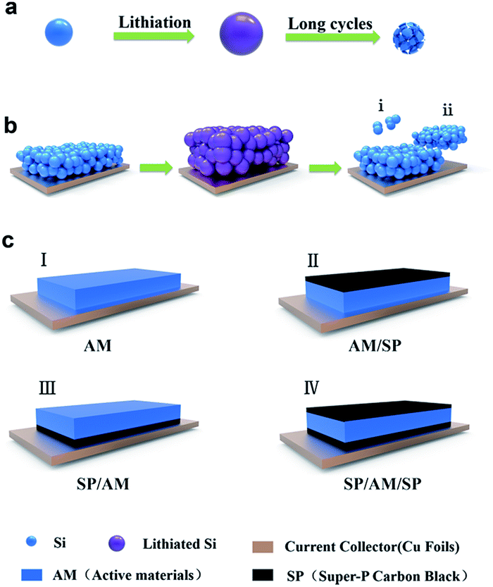 | ||
| Scheme 1 Schematic of failure mechanisms of Si electrodes during the lithiation/delithiation process: (a) cracking and pulverization of the Si particles, (b) delamination and damage of mechanical integrity of the electrodes. (c) Schematic of electrode configurations: (I) a Cu foil, Si/C active materials (abbreviated to AM), (II) a Cu foil, Si/C active materials and UCL (abbreviated as AM/SP), (III) a Cu foil, BCL and Si/C active materials (abbreviated as AM/SP), (IV) a Cu foil, BCL, Si/C AM and UCL (abbreviated as SP/AM/SP). | ||
To overcome these issues, many efforts have been devoted to design rational Si nanostructures and/or coupling with carbon buffers.7,8 On the one hand, various Si nanostructures, including nanoparticles,9,10 nanowires,11,12 nanotubes,13–15 nanosheets,16 Si films,17,18 and hollow Si,19 can substantially accommodate the volume changes within available surrounding void space to prevent fracture formation in the Si particles. On the other hand, carbon buffers in Si/C hybrid nanostructures, such as graphene/rGO encapsulated Si,20,21 Si-MWCNT hierarchical structures,22,23 yolk–shell Si@void@C structures,24 and Si/rGO bilayer nanomembranes,25 act as cushions to accommodate the volume changes to some extent to prevent its pulverization and aggregation. Although the aforementioned works have brought significant improvement to the electrochemical performance, the tedious experimental procedures and costly raw materials greatly hinder their large-scale applications. In this regard, it is necessary to explore some other facile, low cost, and effective methods that are beyond the design and synthesis of the structures of materials.
For an electrochemical device in LIBs, each component, especially the mechanical integrity of the electrodes, plays a vital role in realizing the excellent electrochemical performance. For a Si-based anode, the electrode integrity is mainly dependent on its mechanical strength and internal stress; the integrity failure often results in the loss of electrical contact of Si active materials, which accounts for the origins of the capacity fade.7 Recently, a few studies have revealed that faded capacity of Si could be recovered to its initial capacity when the electrical contact was reconnected by an external force.26 Therefore, retaining the electrode integrity of a Si-based anode is vital for deriving a high capacity and favorable cycling performance.
Recently, a double-layered electrode with a buffer layer between current collector and active materials has been developed for improving the cycling performance of Si,27,28 because the buffer layer can effectively relieve the stress and increase the adhesion strength. Moreover, extensive works on appropriate structured design of electrodes or cell configuration have been reported in researches into lithium–sulfur batteries.29,30 The electrodes or cells usually contain embedded barrier layers between cathode and separator, which can efficiently alleviate the solvation of polysulfide and the shuttle effect. Inspired by these studies, combining the advantages of the buffer layer and the barrier layer will be considered a feasible way to balance the mechanical integrity of the electrode.
Herein, we reported a novel design of Si/C electrode that contains a layer of commercial Si–graphene composite as active materials, which is sandwiched by two conducting carbon layers, as shown in Scheme 1c, IV (abbreviated as SP/AM/SP). The bottom carbon layer (BCL) between the AM and current collector acts as a buffer layer to increase the adhesion strength and avoid peeling-off of the electrode (Scheme 1b, II) caused by its rough surface. The upper carbon layer (UCL) on the electrolyte side acts as a barrier layer to prevent the electrode surface from cracking and delaminating (Scheme 1b, I). The conductive carbon layers on both sides of the AM not only provide excellent electrical conductivity, lowering the impedance of the battery, but also accommodate the volumetric changes during lithiation/delithiation and maintain the electrode integrity. This design can eliminate much more complicated processes and provide potential for commercial application. For comparison, the conventional electrode that bore active materials coated on the Cu foil (abbreviated as AM), the AM/SP electrode (AM with upper SP coated on the Cu foil), and the SP/AM electrode (AM with bottom SP coated on the Cu foil) were also investigated (Scheme 1c, I–III).
Results and discussion
The SEM and TEM images (Fig. 1a and b) show that the Si–graphene composite active materials contain Si nanoparticles and graphene flakes. Crimped and folded graphene flakes form a 3D interconnected network and Si nanoparticles (∼200 nm) are encapsulated in the void spaces of the graphene flakes (Fig. S2†). The interconnected graphene network could serve as the supporting matrix suppressing the agglomeration and pulverization of the Si nanoparticles. This unique structure could provide available void space for the accommodation of the volume changes and enhance charge-transport capabilities during cycling.31,32 To clearly observe the sandwich structure designed, the morphology of a cross-section of the SP/AM/SP electrode is shown in Fig. 1c. The copper foil (∼10 μm) on the bottom serves as current collector and the AM (∼30 μm) is sandwiched by two SP layers (∼10 μm). In addition, the distribution of corresponding elements (Fig. 1d–f), C, Cu, and Si, further confirms the configuration of the sandwich structure. For comparison, the cross sections of the AM, AM/SP, SP/AM electrodes are also given in Fig. S3.†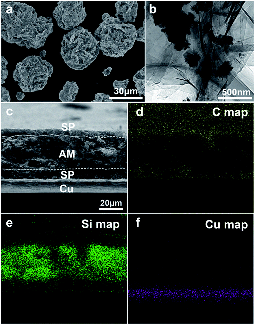 | ||
| Fig. 1 (a) SEM image and (b) TEM image of Si–graphene composite. (c) SEM image, and (d–f) corresponding element mappings of the sandwich-structured electrode. | ||
To investigate the effect of these different configurations on the electrochemical performance, the galvanostatic charge/discharge behaviors of these electrodes were evaluated at a current density of 75 mA g−1 within the voltage range of 0.005–1.2 V (vs. Li+/Li0). The first charge/discharge profiles of the electrodes are shown in Fig. 2a. All the voltage profiles are consistent with other previous studies of Si anodes.6,33 During the first discharge/charge process, a long flat plateau (∼0.1 V) corresponds to the formation of amorphous LixSi, and a relatively short plateau (∼0.4 V) corresponds to the delithiation of LixSi. The initial discharge capacity of the SP/AM/SP electrode is 1736 mA h g−1, which is much higher than that of the SP/AM (1631 mA h g−1), AM/SP (1594 mA h g−1), and AM (1447 mA h g−1) electrodes. It is noted that the capacity of the electrodes increased with the number of SP layers. The increasing capacity should be ascribed to the electrochemical activity of SP as anodes (Fig. S4a†). Moreover, the added SP layers also increase the electronic conductivity to benefit the decrease of the impedance. In contrast, with the increase of the content of SP, the initial Coulomb efficiencies present a slight decrease from 76.6% for AM to 71% for SP/AM/SP (Fig. 2b), which is related to the low initial coulombic efficiency of SP (Fig. S4b†).
 | ||
| Fig. 2 (a) Initial charge–discharge voltage profiles of the different configurations at a current density of 75 mA g−1. (b) Coulombic efficiencies of the different configurations upon cycling. (c) Cycling performance of different configurations at a current density of 0.15 A g−1 after activations prior to cycle 2; open symbols: charge; solid symbols: discharge. (d) Corresponding capacity retentions of the different configurations. | ||
The cycling performances of the electrodes with different configurations are shown in Fig. 2c and d. It is obvious that the SP/AM/SP electrode delivers a high capacity (over 1200 mA h g−1) without any capacity fading after 70 cycles. Nevertheless, the SP/AM, AM/SP, and AM electrodes exhibit some degree of capacity fading from 1200 to 1070 mA h g−1, 1160 to 977 mA h g−1, and 1100 to 920 mA h g−1, respectively. Interestingly, the capacity retention of SP/AM/SP exceeds 100%. This result may originate from the electrochemical activation upon cycling,34 which is induced by the poor electrolyte wettability with the thick SP/AM/SP electrode. At the same time, the cycling stability of the SP/AM configuration with the BCL shows more excellent performance than that of AM/SP configuration with the UCL. This implies that the BCL is more effective than UCL for the improvement of cycling performance. Moreover, the superior cycling performance of the SP/AM/SP configuration can result from synergy between SP layers on both sides of the AM.
In general, the process of large volume changes upon lithiation/delithiation not only leads to cracking and pulverization of the Si particles, but causes failure at the level of the entire electrode.7 In order to reveal the mechanism of the enhancement of cycling performance for the sandwich-structured Si/C configuration, the structural states of the electrodes before and after cycling were investigated. The cross sections of the electrodes with different configurations before cycling are presented in Fig. 3a–d. It is clearly observed that there is a tiny gap between the AM and Cu foil in the configuration of AM and AM/SP (Fig. 3a and b), whereas it is invisible for the SP/AM/SP and SP/AM configurations (Fig. 3c and d). This indicates that the BCL as a buffer layer can increase the adhesion of the active materials to the Cu foil due to its rough surface (Fig. S5†). In contrast, the cross sections of the electrodes after cycling (Fig. 3e–h) show that the Cu foil is out of the bottom of the AM and AM/SP configurations, indicating a poor adhesion between them, whereas the SP/AM and SP/AM/SP configurations still exhibit good adhesion to the Cu foil. The cross-sectional SEM images of electrodes at the fully discharged state are also provided in Fig. S6,† which show similar results. Furthermore, the integrity of the electrodes after cycling is also compared in Fig. 3i–l. These results demonstrate that electrodes with the BCL can prevent the exfoliation of the active materials from the Cu foil to maintain electrode integrity upon cycling, which plays an important role in the improvement of the electrochemical performance.
 | ||
| Fig. 3 The cross-section morphologies of electrodes: (a–d) before cycling and (e–h) after 70 cycles, for AM, AM/SP, SP/AM, SP/AM/SP, respectively. The typical photographs of electrodes after 70 cycles: (i) AM, (j) AM/SP, (k) SP/AM, (l) SP/AM/SP. | ||
During the cycling process, Si particles suffer from repeated expansion and contraction, resulting in detachment from the surrounding electrical connections, especially the surface of the electrode.7,13 This drastic electrode morphology change can further contribute to capacity fading. The laser scanning confocal microscope (LSCM), commonly used in cell biology for location detection and cytometry, was used to reveal the surface morphology changes of electrodes with three-dimensional images (Fig. 4).35 Before cycling, the AM/SP and SP/AM/SP with UCL show a smoother surface than the AM and SP/AM. As a barrier, the UCL is made up of SP and PVDF, in which many micro pores can provide the diffusion path for lithium ions. After cycling, the AM and AM/SP without UCL exhibit partial cracking and delamination (Fig. 4b and f), whereas the AM/SP and SP/AM/SP still show good integrity (Fig. 4d and h). The surface SEM images of the electrodes before and after cycling are also provided in Fig. S7.† These results suggest that the UCL as a barrier layer can maintain the active materials' attachment and their electrical connections.
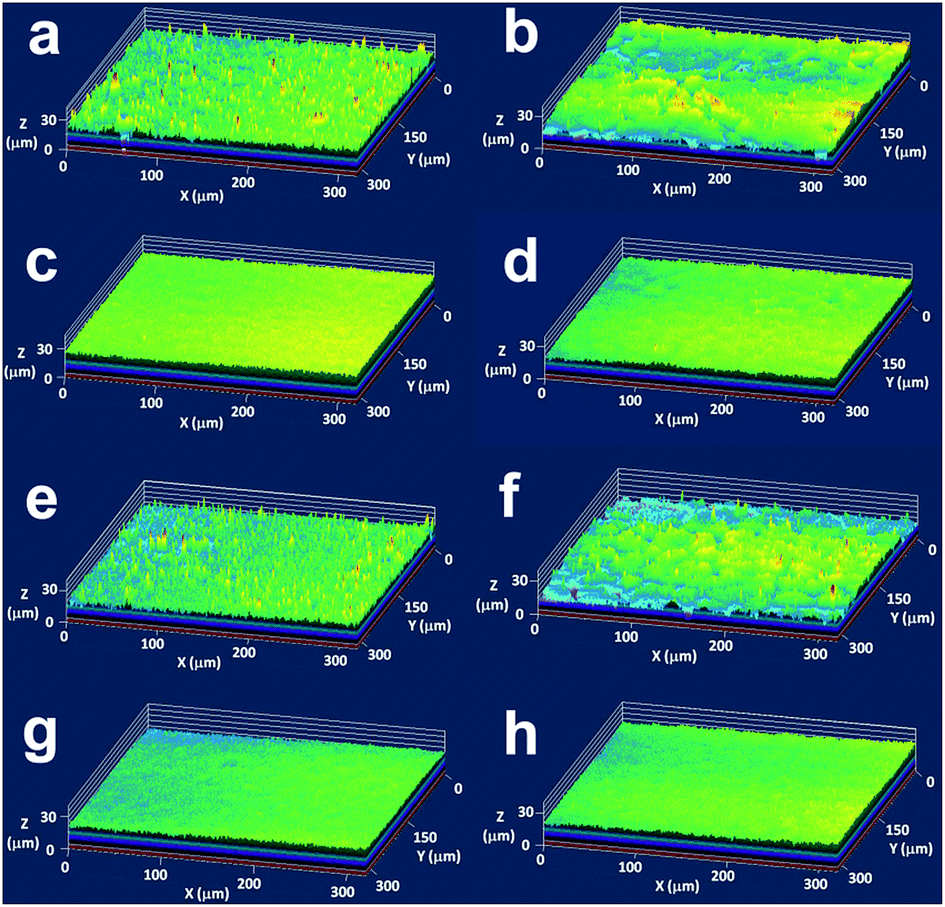 | ||
| Fig. 4 Laser scanning confocal microscope (LSCM) images of surface morphology of the electrodes with different configurations before (left) and after cycling (right): (a and b) AM, (c and d) AM/SP, (e and f) SP/AM, (g and h) SP/AM/SP. | ||
The electrochemical impedance spectra (EIS) of the electrodes are also compared after different cycles (Fig. 5a and b). The Nyquist plots for these electrodes consist of a single depressed semicircle in the high-to-medium frequency region and an inclined line in the low-frequency region. The plots can be simplified by an equivalent circuit (the inset of Fig. 5a). In the equivalent circuit, RΩ, CPE, Rct, and W0 represent the electrolyte resistance, constant phase element, charge transfer resistance, and Warburg impedance, respectively.36,37 The calculated values of RΩ and Rct for the different electrodes with various cycle numbers are shown in Table 1. After 2 cycles of activation, the calculated RΩ of the four electrodes range from 2 to 3 Ω, indicating that the initial condition of the electrolytes is similar. The calculated value of Rct for SP/AM/SP (14.1 Ω) is lower than that for AM (29.1 Ω), AM/SP (17.7 Ω) and SP/AM (14.4 Ω), suggesting a faster charge transfer for the SP/AM/SP configuration. After 50 cycles, the calculated RΩ of the four electrodes increase to about 18 Ω, which can be ascribed to the formation of the SEI upon cycling. The Rct of SP/AM/SP (9.0 Ω) shows slight reduction, which can be ascribed to maintaining integrity of the electrode and the slow activation phenomenon.34 However, the Rct of AM, AM/SP and SP/AM increases upon cycling, which is ascribed to the failure of the electrodes. The result is consistent with an amplified diameter of the semicircles (Fig. 5b). In conclusion, the BCL can function as buffer layer with good conductivity and a rough surface, increasing the contact surface area and lowering the charge-transfer resistance (Rct). Moreover, the UCL acts as an embedded current collector, maintaining the integrity of electrode surface.
 | ||
| Fig. 5 Nyquist plots of the different electrodes with various cycle numbers: (a) after two cycles and (b) after 50 cycles from 10 kHz to 10 mHz at room temperature. Inset of (a) is the simplified electrochemical system as a Randles circuit, in which RΩ, CPE, Rct, and W0 are the electrolyte resistance, constant phase element, charge transfer resistance, and Warburg impedance, respectively. | ||
| Elements | RΩ (Ω) | RΩ (Ω) | Rct (Ω) | Rct (Ω) |
|---|---|---|---|---|
| Cycles | 2 | 50 | 2 | 50 |
| AM | 2.7 | 18.6 | 29.1 | 41.7 |
| AM/SP | 2.4 | 19.3 | 17.7 | 22.1 |
| SP/AM | 2.9 | 17.8 | 14.4 | 15.1 |
| SP/AM/SP | 2.0 | 20.3 | 14.1 | 9.0 |
To further confirm the effect of the sandwich structure, the active material, Si–graphene, in the electrodes was replaced by Si–graphite obtained in the same manner. Electrodes containing Si–graphite with the sandwich structure and the conventional single layer were fabricated in the same way as mentioned above. As shown in Fig. 6a, the sandwich structure electrode exhibits better cycling performance than the single layer electrode, which is consistent with the results obtained. It was also reported that an increased amount of conductive carbon or a reduced amount of silicon in an electrode is favorable for the electrochemical performance.38 The percentages of Si–graphene and SP in the sandwich structure electrode are 55% and 34%, respectively. Such a single layer electrode with the same proportion (Si–graphene 55%, SP 34%, and PVDF 11%) was also prepared and tested. The electrode with a sandwich structure still represents better cycling performance than that of single layer electrode, indicating that the sandwich structure indeed improves the cycling performance (Fig. 6b). It is noted that the two types of electrodes with the same amount of Si, but different electrode structures, deliver distinct cycling performances, demonstrating that the structure of the electrode can significantly influence the electrochemical performance.
 | ||
Fig. 6 The cycling performance of electrodes with a different structure: (a) Si/graphite as the active material of the electrodes, (b) Si–graphene as the active material of electrodes with the same proportion (Si–graphene![[thin space (1/6-em)]](https://www.rsc.org/images/entities/char_2009.gif) :SP:PVDF = 55:34:11). :SP:PVDF = 55:34:11). | ||
Experimental
Synthesis of Si–graphene composite
Commercial silicon (500 g, 200 mesh) and polyacrylic acid (100 g, Sinopharm Chemical Reagent Co., Ltd) were ball-milled in an aqueous solution to reduce the particle size to about 200 nm. The XRD patterns before and after ball-milling are provided in the ESI (Fig. S1†). Furthermore, graphene (200 g, Ningbo Morsh Technology Co., Ltd) and glucose (100 g, Sinopharm Chemical Reagent Co., Ltd) were added to the abovementioned mixture to form a suspension (the solid content was 10 wt%). The suspension was subsequently spray dried with an inlet air temperature of 200 °C to form a solid. The prepared solid powders were annealed at 800 °C for 4 h under an argon atmosphere at a heating rate of 5 °C min−1 followed by natural cooling.Electrode fabrication
For the fabrication of the electrodes with different configurations, a Si–graphene slurry (80 wt% Si–graphene, 10 wt% carbon black (Super P), and 10 wt% PVDF) and a conductive carbon slurry (80 wt% carbon black (Super P), 20 wt% PVDF) were prepared. The AM electrode was fabricated by coating the Si–graphene slurry onto a Cu foil and dried in an oven at 80 °C. The AM/SP electrode was fabricated by coating the conductive carbon slurry onto the AM electrode and then drying in an oven at 80 °C. The SP/AM electrode was fabricated by a similar process used for the AM/SP electrode with the order of the coatings reversed. The SP/AM/SP electrode was fabricated by coating the conductive carbon slurry onto the SP/AM electrode and then drying in an oven at 80 °C. The electrodes were cut, compressed and shaped into circular slices with a diameter of 13 mm. The average mass loading of the AM, AM/SP, SP/AM and SP/AM/SP electrodes was 1.91 mg cm−2, 2.21 mg cm−2, 2.29 mg cm−2 and 3.01 mg cm−2, respectively.Materials characterization
Scanning electron microscopy (SEM) was performed using a Hitachi S-4800 (8 kV) and an FEI Quanta FEG 250 (20 kV). EDXS was used for elemental analysis. Transmission electron microscopy (TEM) was performed in an FEI Tecnai F20 at an accelerating voltage of 200 kV. The surface roughness of the electrodes was determined by a Dimension 3100 V (Veeco, USA) scanning probe microscope (SPM). The surface 3D morphologies of the electrodes were obtained by a Leica TCS SP5 laser scanning confocal microscope (LSCM).Electrochemical measurements
Electrochemical tests were carried out in CR2032-type coin cells. A lithium metal foil was used as the anode, Celgard 2400 microporous membrane as the separator, and the electrolyte was 1 M LiPF6 dissolved in a mixed solvent of ethylene carbonate (EC) and diethyl carbonate (DEC) (1:1 by volume, Guotai-Huarong New Chemical Material Co., Ltd). The coin-type cells were assembled in an Ar-filled glove box (H2O < 0.1 ppm, O2 < 0.1 ppm). All the cells were tested under different current densities within the voltage range of 0.005–1.2 V using a LAND-CT2001A battery test system (Jinnuo Wuhan Corp., China). Electrochemical impedance spectroscopy (EIS) analysis was performed on an electrochemical workstation (Solartron Analytical, 1470E, UK) within the frequency range from 0.01 to 100 kHz.
Conclusions
In this study, a simple and effective strategy for improving cycling performance of Si-based anodes is proposed. The electrodes with a sandwich structure exhibit much better capacity retention and lower charge transfer resistance compared to conventional single layer electrodes. The carbon layers on both sides of the electrode play a synergetic role in maintaining the mechanical integrity of the entire electrode, including improvement in the cycling performance. The BCL serves as a buffer layer; results show enhancement of adhesion of the active material to the Cu foil. The UCL acts as a protective layer, preventing the active materials from peeling off. Finally, we conclude that our reported design provides a simple manufacturing scheme for production of a high performance Si-based anode on a large scale, which would constitute a promising, cost-effective future industrial application.Acknowledgements
This study was supported by the China Postdoctoral Science Foundation (Grant No. 2015T80641), the Strategic Priority Research Program of Chinese Academy of Sciences (CAS, Grant No. XDA09010101), and the Ningbo Industrialization Application Development Program of Graphene (Grant No. 2015S1002).Notes and references
- J. M. Tarascon and M. Armand, Nature, 2001, 414, 359 CrossRef CAS PubMed.
- M. Armand and J. M. Tarascon, Nature, 2008, 451, 652 CrossRef CAS PubMed.
- J. B. Goodenough and Y. Kim, Chem. Mater., 2010, 22, 587 CrossRef CAS.
- P. G. Bruce, B. Scrosati and J.-M. Tarascon, Angew. Chem., Int. Ed., 2008, 47, 2930 CrossRef CAS PubMed.
- M. S. Whittingham, Chem. Rev., 2004, 104, 4271 CrossRef CAS PubMed.
- U. Kasavajjula, C. Wang and A. J. Appleby, J. Power Sources, 2007, 163, 1003 CrossRef CAS.
- H. Wu and Y. Cui, Nano Today, 2012, 7, 414 CrossRef CAS.
- M. L. Terranova, S. Orlanducci, E. Tamburri, V. Guglielmotti and M. Rossi, J. Power Sources, 2014, 246, 167 CrossRef CAS.
- N. Lin, Y. Han, L. Wang, J. Zhou, J. Zhou, Y. Zhu and Y. Qian, Angew. Chem., 2015, 54, 3822 CrossRef CAS PubMed.
- L. Wang, N. Lin, J. Zhou, Y. Zhu and Y. Qian, Chem. Commun., 2015, 51, 2345 RSC.
- C. K. Chan, H. Peng, G. Liu, K. McIlwrath, X. F. Zhang, R. A. Huggins and Y. Cui, Nat. Nanotechnol., 2008, 3, 31 CrossRef CAS PubMed.
- Y. Xiao, D. Hao, H. Chen, Z. Gong and Y. Yang, ACS Appl. Mater. Interfaces, 2013, 5, 1681 CAS.
- T. Song, J. Xia, J.-H. Lee, D. H. Lee, M.-S. Kwon, J.-M. Choi, J. Wu, S. K. Doo, H. Chang, W. Il Park, D. S. Zang, H. Kim, Y. Huang, K.-C. Hwang, J. A. Rogers and U. Paik, Nano Lett., 2010, 10, 1710 CrossRef CAS PubMed.
- M.-H. Park, M. G. Kim, J. Joo, K. Kim, J. Kim, S. Ahn, Y. Cui and J. Cho, Nano Lett., 2009, 9, 3844 CrossRef CAS PubMed.
- A. T. Tesfaye, R. Gonzalez, J. L. Coffer and T. Djenizian, ACS Appl. Mater. Interfaces, 2015, 7, 20495 CAS.
- Z. Lu, J. Zhu, D. Sim, W. Zhou, W. Ship, H. H. Hng and Q. Yan, Chem. Mater., 2011, 23, 5293 CrossRef CAS.
- J. P. Maranchi, A. F. Hepp and P. N. Kumta, Electrochem. Solid-State Lett., 2003, 6, A198 CrossRef CAS.
- F. Qu, C. Li, Z. Wang, H. P. Strunk and J. Maier, ACS Appl. Mater. Interfaces, 2014, 6, 8782 CAS.
- Y. Yao, M. T. McDowell, I. Ryu, H. Wu, N. A. Liu, L. B. Hu, W. D. Nix and Y. Cui, Nano Lett., 2011, 11, 2949 CrossRef CAS PubMed.
- N. Lin, J. B. Zhou, L. B. Wang, Y. C. Zhu and Y. T. Qian, ACS Appl. Mater. Interfaces, 2015, 7, 409 CAS.
- X. Zhou, Y.-X. Yin, L.-J. Wan and Y.-G. Guo, Adv. Energy Mater., 2012, 2, 1086 CrossRef CAS.
- P. Gao, Y. Nuli, Y.-S. He, J. Wang, A. I. Minett, J. Yang and J. Chen, Chem. Commun., 2010, 46, 9149 RSC.
- P. Gao, H. Jia, J. Yang, Y. Nuli, J. Wang and J. Chen, Phys. Chem. Chem. Phys., 2011, 13, 20108 RSC.
- N. Liu, H. Wu, M. T. McDowell, Y. Yao, C. M. Wang and Y. Cui, Nano Lett., 2012, 12, 3315 CrossRef CAS PubMed.
- X. Liu, J. Zhang, W. Si, L. Xi, B. Eichler, C. Yan and O. G. Schmidt, ACS Nano, 2015, 9, 1198 CrossRef CAS PubMed.
- J. H. Ryu, J. W. Kim, Y.-E. Sung and S. M. Oh, Electrochem. Solid-State Lett., 2004, 7, A306 CrossRef CAS.
- S. Lee and E.-S. Oh, J. Power Sources, 2013, 244, 721 CrossRef CAS.
- Y. Xu, G. Yin, X. Cheng and P. Zuo, Electrochim. Acta, 2011, 56, 4403 CrossRef CAS.
- J. Song, Z. Yu, T. Xu, S. Chen, H. Sohn, M. Regula and D. Wang, J. Mater. Chem. A, 2014, 2, 8623 CAS.
- G. Zhou, S. Pei, L. Li, D. W. Wang, S. Wang, K. Huang, L. C. Yin, F. Li and H. M. Cheng, Adv. Mater., 2014, 26, 625 CrossRef CAS PubMed.
- Q. Zhu, P. Wu, J. Zhang, W. Zhang, Y. Zhou, Y. Tang and T. Lu, ChemSusChem, 2015, 8, 131 CrossRef CAS PubMed.
- P. Wu, H. Wang, Y. Tang, Y. Zhou and T. Lu, ACS Appl. Mater. Interfaces, 2014, 6, 3546 CAS.
- M. T. McDowell, S. W. Lee, W. D. Nix and Y. Cui, Adv. Mater., 2013, 25, 4966 CrossRef CAS PubMed.
- H. C. Shin, J. A. Corno, J. L. Gole and M. L. Liu, J. Power Sources, 2005, 139, 314 CrossRef CAS.
- M. Kozubek, S. Kozubek, E. Lukasova, A. Mareckova, E. Bartova, M. Skalnikova and A. Jergova, Cytometry, 1999, 36, 279 CrossRef CAS PubMed.
- S.-L. Chou, J.-Z. Wang, M. Choucair, H.-K. Liu, J. A. Stride and S.-X. Dou, Electrochem. Commun., 2010, 12, 303 CrossRef CAS.
- W.-R. Liu, J.-H. Wang, H.-C. Wu, D.-T. Shieh, M.-H. Yang and N.-L. Wu, J. Electrochem. Soc., 2005, 152, A1719 CrossRef CAS.
- N. Ding, J. Xu, Y. Yao, G. Wegner, I. Lieberwirth and C. Chen, J. Power Sources, 2009, 192, 644 CrossRef CAS.
Footnote |
| † Electronic supplementary information (ESI) available: (Fig. S1) The XRD patterns of commercial silicon before and after ball-milling; (Fig. S2) the morphological and structural characterization of the Si/graphene composite; (Fig. S3) cross sections images and corresponding element mapping of AM, AM/SP and SP/AM; (Fig. S4) first charge/discharge voltage profiles, coulombic efficiency and cycling performance of SP; (Fig. S5) SPM images of the surface of Cu foil and SP; (Fig. S6) the cross-sectional SEM images of electrodes at full discharged state; (Fig. S7) the surface SEM of the electrodes with different configurations before and after cycling. See DOI: 10.1039/c5ra23283j |
| This journal is © The Royal Society of Chemistry 2016 |