Proton gated oxide electric-double-layer transistors for full-swing low voltage inverter applications

Hui Xiao, Li Qiang Zhu*, Yang Hui Liu and Rui Liu
Ningbo Institute of Materials Technology and Engineering, Chinese Academy of Sciences, Ningbo 315201, People's Republic of China. E-mail: lqzhu@nimte.ac.cn

Received 4th November 2015 , Accepted 16th December 2015

First published on 18th December 2015


Abstract

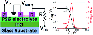
Ion gated electric-double-layer (EDL) transistors provide promising strategies to achieve electrostatic modulation for solid-state materials. Here, proton gated indium-zinc-oxide (IZO) EDL transistors were fabricated by using nanogranular phosphorosilicate glass (PSG) based electrolytes as gate dielectrics. A high proton conductivity of ∼3.9 × 10⁻⁴ S cm−1 and an extremely big EDL capacitance of ∼4.4 μF cm−2 were observed for the PSG based electrolyte. The IZO EDL transistors could operate at a low voltage of 1.5 V. Furthermore, resistor-loaded inverters were built, demonstrating modulatable electrical performances by a modulatable operation mode of the driving IZO transistor. Full-swing inverter characteristics were observed at a low supply voltage of 1.5 V, exhibiting a high voltage gain of above 7. The inverters were also used for decreasing the noises of input signals. The proton gated oxide EDL transistors have potential applications in biochemical sensors and portable electronics.


I Introduction

Ionic-liquid or ionic-gel electrolyte gated transistors (EGTs) provide promising strategies to translate ionic signals into easily detectable electron signals and to achieve electrostatic modulations for solid-state materials.1–3 Under an external electrical-field, strong electrostatic coupling is expected between mobile ions within ionic-liquid or ionic-gel electrolytes and carriers within solid-state channels.4,5 Due to the formation of an electric-double-layer (EDL) at the interface with a big capacitance of >1.0 μF cm−2, the EGTs could operate at low voltage (<2 V).6,7 The unique properties for EGTs are that they could induce carriers with an extremely high density of ∼1014 cm−2 by merely tuning gate voltage, being free from structural disorders inherent with chemical doping. Recently, solid-state electrolytes gated oxide EDL transistors have been reported.8–13 Dynamic characteristics of ion gating for the electrolytes were studied.14,15 With unique ionic/electronic hybrid behaviors, these electrolytes gated EDL transistors have been proposed as artificial synapses for neuromorphic system applications.16,17 At the same time, inverters are fundamental elements in logic circuits, integrated systems and sensors.18,19 Inverters utilizing p-channel organic transistor and n-channel oxide transistor19,20 and inverters utilizing n-channel oxide transistors with different threshold voltages21,22 have been reported. However, most of them require complicated processings and are driven at relatively high voltages.21–23 Thus, it is of interest to build inverters with simple processings. Fortunately, electrolytes gated EDL transistors could operate at low voltage and could be fabricated with simple processings. They could potentially act as drivers in low-voltage inverters for portable applications. In our previous work, EDL transistors have been proposed for inverter applications.24,25 However, modulating inverter performances and processing noise signals have not been addressed and are needed to be discussed.

In the present work, proton gated low-voltage oxide EDL transistors are fabricated at room temperature. Resistor-loaded inverters are built by connecting proton gated EDL transistors in series with resistors, illustrating high voltage gains of above 7 at low operation voltage. Electric performances of the inverters are modulated. The inverter is also used for decreasing noises of input signals.

II Experimental section

Indium-zinc-oxide (IZO) EDL transistors were fabricated at room temperature. First, nanogranular phosphorosilicate glass (PSG) electrolyte films with thickness (D) of ∼1.3 μm were deposited on ITO glass substrates by plasma enhanced chemical vapour deposition (PECVD). SiH4 (94% SiH4 + 6% PH3) and O2 were used as reactive gases. Then, patterned IZO films were deposited on PSG electrolytes by radio-frequency (RF) magnetron sputtering IZO target in pure Ar ambient with a gradient metal shadow mask, as schematically shown in Fig. 1. When distance between the IZO patterns is 80 μm, a thin IZO layer can be self-assembled between the patterns due to reflection of IZO nanoparticles at mask edge and dimensional extension by IZO nanoparticles with a low incident angle. When distance between the IZO patterns is 300 μm, isolated IZO patterns could be obtained. The IZO patterns with the self-assembled IZO layer could be deemed as source and drain electrodes. The self-assembled IZO layer could be deemed as channel. The isolated IZO pattern could be deemed as gate electrode. Thus, proton gated IZO transistors are obtained. Capacitive gating effects were coupled to IZO channel via a bottom ITO layer. The channel width (W) and length (L) are 1 mm and 80 μm, respectively. The channel thicknesses could be modulated by changing distances between the metal mask and the substrate. Resistor-loaded inverters were built by connecting IZO transistors in series with resistors (4 MΩ), as schematically shown in Fig. 5(a). Proton conductivity (σ) and frequency dependent capacitance of the PSG electrolyte were characterized with impedance analyzer. Hall-effect measurements were performed for IZO films deposited on quartz substrates. Chemical composition of IZO film was analyzed with X-ray photoelectron spectroscopy (XPS). Electrical performances of the IZO transistors and the resistor-loaded inverters were characterized by Keithley 4200 semiconductor parameter analyzer at room temperature.
image file: c5ra23155h-f1.tif
Fig. 1 Schematic diagram to obtain IZO transistors with different channel thicknesses by adopting a gradient mask method.

III Results and discussion

Proton conductivity (σ) of the PSG electrolyte was determined by using an IZO/PSG/ITO sandwich structure. Fig. 2(a) shows impedance spectroscopy data collected as real (Re Z′) and imaginary (Im Z′′) components of the complex impedance. Impedance real value (R) of ∼240 Ω is obtained with impedance imaginary value equal to zero. Proton conductivity (σ) could be obtained from the relation below:
image file: c5ra23155h-t1.tif
where A of ∼1.5 × 10⁻³ cm2 is electrode area and R0 of ∼20 Ω is resistance of electrode, respectively. Thus, σ is estimated to be ∼3.9 × 10⁻⁴ S cm−1. Fig. 2(b) shows frequency dependent specific capacitance for the PSG electrolyte. An electric-double-layer (EDL) capacitance (C) of ∼4.4 μF cm−2 is obtained at 1.0 Hz. The big EDL capacitance provides a strong electrostatic coupling effect between gate and IZO channel.

image file: c5ra23155h-f2.tif
Fig. 2 (a) Impedance spectroscopy dada of the nanogranular PSG electrolyte. Inset: an IZO/PSG/ITO sandwich structure for measurements. (b) Capacitance–frequency curve for the nanogranular PSG electrolyte. Inset: in-plane sandwich structure for measurements.

Fig. 3(a) shows typical output curves (Ids vs. Vds) for proton gated IZO transistor with channel thickness of ∼20 nm. At low Vds, Ids increases linearly with Vds, indicating that the device has a good ohmic contact. At higher Vds, Ids gradually saturates. Fig. 3(b) illustrates transfer curves (Ids vs. Vgs) for proton gated IZO transistors with channel thickness of ∼32, ∼20 and ∼12 nm, respectively. Vgs is swept with a constant Vds at 1.5 V. A small anticlockwise hysteresis loop of ∼0.2 V is observed between forward and reverse Vgs scans, which is related to mobile protons within the PSG electrolyte.16,26 These results clearly indicate that the IZO transistors could operate at low voltage of 1.5 V. Moreover, there are positive shifts in transfer curves with decreased channel thicknesses. Table 1 illustrates electrical parameters extracted from the transfer curves. All the devices show a small subthreshold swing (SS) scattered between 110 and 117 mV per decade. When channel thicknesses decrease from 32 to 12 nm, field-effect mobilities (μ) decrease from ∼13.5 to ∼5.5 cm2 V−1 s−1, while threshold voltages (Vth) increase from −0.1 to 0.4 V. The electrical performances obtained here are comparable to those for the reported solid-state electrolyte gated oxide transistors.13,25,27


image file: c5ra23155h-f3.tif
Fig. 3 (a) Typical output curves (Ids vs. Vds) of proton gated IZO transistor. IZO channel thickness is ∼20 nm. (b) Transfer characteristics (Ids vs. Vgs) for different channel thicknesses of ∼32, ∼20 and ∼12 nm, respectively.
Table 1 Comparisons of electrical parameters for the proton gated IZO transistors with different channel thicknesses
Channel thickness (nm) 32 20 12
SS (mV per decade) 117 112 113
ION/OFF 5.1 × 10⁵ 1.1 × 10⁶ 2.2 × 10⁶
Vth (V) −0.1 0.3 0.4
μ (cm2 V−1 s−1) 13.5 6.0 5.5


The changes in electrical performances could be explained as follows. Fig. 4(a) illustrates carrier densities as a function of IZO film thicknesses. It is observed that the carrier densities decrease from ∼2.7 × 1015 cm−2 to ∼1.9 × 1014 cm−2 with IZO film thicknesses decrease from ∼62 nm to ∼12 nm. The observations indicate that there are decreased carrier numbers in thinner IZO channels, which induces positive shifts in Vth for IZO transistors with thinner IZO channels.28 Fig. 4(b) shows O 1s core level XPS spectrum taken from IZO film. Four components are observed, centred at ∼529.8 eV, ∼530.6 eV, ∼531.8 eV and ∼532.9 eV, respectively. The components centred at 529.8 eV and 530.6 eV are attributed to ionic O bonds, i.e., [O]–In and [O]–Zn, respectively. The component centred at 531.8 eV is attributed to oxygen-deficient chemical state. While the component centred at 532.9 eV is attributed to surface species (H2O, O2). When IZO channels are exposed to atmosphere ambient, moistures within atmosphere could be inevitably absorbed on the channel surfaces. Some of H2O molecules could be transformed into OH species through an interaction with IZO layer. Such OH species could take electrons from IZO channel to form OH species, as shown in Fig. 4(c).29 Moreover, oxygen species existed within atmosphere will also be absorbed on the channel surfaces. Such oxygen species will be negatively charged by capturing free electrons (e).30 When channel thicknesses decrease, the changes in electron concentrations will get significant, which depletes the channels and results in the positive shifts in Vth.31 Moreover, surface species would act as scattering centres for channel carriers. When the channel thicknesses decrease, the effects of such scattering on mobility would get significant. Thus, the μ values will decrease.


image file: c5ra23155h-f4.tif
Fig. 4 (a) Carrier densities as a function of IZO film thicknesses. (b) O 1s XPS spectrum for IZO film. (c) Schematic diagram of the formation of negatively charged oxygen species (O2−) and hydroxyl species (OH).

The promising electrical performances of the proton gated IZO EDL transistors allow their potential applications in logic circuits. Fig. 5(a) schematically illustrates a resistor-loaded inverter. Fig. 5(b) shows static voltage transfer characteristics (VTC) of inverters taken under a constant supply voltage (VDD) of 1.5 V. Channel thicknesses of driving transistors are 32, 20 and 12 nm, respectively. All the inverters demonstrate full-swing characteristics. Fig. 5(c) shows voltage gains (|dVout/dVin|) of the inverters. A maximum voltage gain of ∼9.4 is obtained when the channel thickness is 32 nm. While a voltage gain of ∼8.4 is obtained when the channel thickness is 12 nm. These values are comparable to those of inverters driven by ionic-gel and chitosan gated transistors.15,32 It is interesting to note here that a high VDD is needed to obtain a comparable voltage gain for the reported depletion-loaded inverter. In ref. 33, voltage gain was reported to be ∼10 at VDD of 6 V for depletion-loaded inverter using ZnSnO transistor and SiZnSnO transistor. While in ref. 34, voltage gain was reported to be ∼17 at VDD of 10 V for depletion-loaded InGaZnO inverter. Thus, our results indicate high potentials for the proposed inverters in portable applications. Furthermore, transition width values of ∼0.3 V are also extracted from the VTC curves. Such values are also much lower than that for the reported depletion-loaded inverters.33,34 Interestingly, the VTC curves shift to positive directions with decreased channel thicknesses, which are related to the increased Vth values for driving IZO transistors with decreased channel thicknesses. For portable electronics and chemical sensor applications, noises inevitably exist. To improve signal-noise ratio, the noise should be decreased. Fig. 5(d) shows the output characteristics of the inverter for noise input signals with IZO channel thickness of 32 nm. The inverter converts noise input signals into two-bit outputs. These results convince that the proton gated IZO transistors could act as fundamental building blocks for potential applications in portable electronics.


image file: c5ra23155h-f5.tif
Fig. 5 (a) Schematic diagram of a resistor loaded inverter. (b) Static voltage transfer characteristics (VTC) and (c) voltage gain (|dVout/dVin|) of resistor-loaded inverters with different channel thicknesses for driving IZO transistors. (d) Output characteristics of the inverter for noise input signals with IZO channel thickness of ∼32 nm.

IV Conclusions

In summary, proton gated indium-zinc-oxide (IZO) EDL transistors are fabricated by using nanogranular phosphorosilicate glass (PSG) electrolytes as gate dielectrics. Resistor-loaded inverters are constructed by connecting resistors in series with proton gated IZO EDL transistors. Due to the strong EDL effects for PSG electrolytes, proton gated IZO EDL transistors could operate at low voltage. Operation modes of the proton gated IZO transistors were modulated with channel thicknesses. Thus, electrical performances of the inverters were modulated correspondingly. The inverters exhibit full-swing characteristics with high voltage gains of above 7 and good switching characteristics at low supply voltage of 1.5 V. Furthermore, the inverters exhibit the function of decreasing noises of input signals. Proton gated oxide EDL transistors with modulatable electric performances have potential applications in biochemical sensors and portable electronics.

Acknowledgements

The authors are grateful for the financial supports from the National Natural Science Foundation of China (11474293), the National Program on Key Basic Research Project (2012CB933004), the Zhejiang Provincial Natural Science Foundation of China (LY14A040009) and Youth Innovation Promotion Association CAS and CAS Interdisciplinary Innovation Team.

References

  1. A. Facchetti, Nat. Mater., 2008, 7, 839 CrossRef CAS PubMed.
  2. K. Ueno, S. Nakamura, H. Shimotani, A. Ohtomo, N. Kimura, T. Nojima, H. Aoki, Y. Iwasa and M. Kawasaki, Nat. Mater., 2008, 7, 855 CrossRef CAS PubMed.
  3. K. Ueno, S. Nakamura, H. Shimotani, H. T. Yuan, N. kimura, T. Nojima, H. Aoki, Y. Iwasa and M. Kawasaki, Nat. Nanotechnol., 2011, 6, 408 CrossRef CAS PubMed.
  4. S. Bubel, M. S. Menyo, T. E. Mates, J. H. Waite and M. L. Chabinyc, Adv. Mater., 2015, 27, 3331 CrossRef CAS PubMed.
  5. Y. Wada, J. Pu and T. Takenobu, Appl. Phys. Lett., 2015, 107, 153505 CrossRef.
  6. S. H. Kim, K. Hong, W. Xie, K. H. Lee, S. P. Zhang, T. P. Lodge and C. D. Frisbie, Adv. Mater., 2013, 25, 1822 CrossRef CAS PubMed.
  7. H. T. Yuan, H. Shimotani, J. T. Ye, S. Yoon, H. Aliah, A. Tsukazaki, M. Kawasaki and Y. Iwasa, J. Am. Chem. Soc., 2010, 132, 18402 CrossRef CAS PubMed.
  8. J. Jiang, Q. Wan, J. Sun and A. X. Lu, Appl. Phys. Lett., 2009, 95, 152114 CrossRef.
  9. G. D. Wu, J. M. Zhou, H. L. Zhang, L. Q. Zhu and Q. Wan, IEEE Electron Device Lett., 2012, 33, 1720 CrossRef CAS.
  10. H. L. Zhang, L. Q. Guo and Q. Wan, J. Mater. Chem. C, 2013, 1, 2781 RSC.
  11. T. Tsuchiya, S. Moriyama, K. Terabe and M. Aono, Appl. Phys. Lett., 2015, 107, 103104 CrossRef.
  12. T. Tsuchiya, M. Ochi, T. Higuchi, K. Terabe and M. Aono, ACS Appl. Mater. Interfaces, 2015, 7, 12254 CAS.
  13. L. Q. Zhu, H. Xiao and J. X. Wang, J. Phys. D: Appl. Phys., 2016, 49, 025104 CrossRef.
  14. N. Liu, L. Q. Zhu, H. Xiao, C. J. Wan, Y. H. Liu and J. Y. Chao, ACS Appl. Mater. Interfaces, 2015, 7, 6205 CAS.
  15. J. Y. Chao, L. Q. Zhu, H. Xiao and Z. G. Yuan, IEEE Electron Device Lett., 2015, 36, 799 CrossRef CAS.
  16. L. Q. Zhu, C. J. Wan, L. Q. Guo, Y. Shi and Q. Wan, Nat. Commun., 2014, 5, 3158 Search PubMed.
  17. Z. J. Guo, L. Q. Guo, L. Q. Zhu and Y. J. Zhu, J. Mater. Sci. Technol., 2014, 30, 1411 Search PubMed.
  18. Y. V. Li, J. I. Ramirez, K. G. Sun and T. N. Jackson, IEEE Electron Device Lett., 2013, 34, 891 CrossRef CAS.
  19. H. Wang, L. Yu, Y. H. Lee, Y. Shi, A. Hsu, M. L. Chin, L. J. Li, M. Dubey, J. Kong and T. Palacios, Nano Lett., 2012, 12, 4674 CrossRef CAS PubMed.
  20. K. Nomura, T. Aoki, K. Nakamura, T. Kamiya, T. Nakanishi, T. Hasegawa, M. Kimura, T. Kawase, M. Hirano and H. Hosono, Appl. Phys. Lett., 2010, 96, 263509 CrossRef.
  21. P. C. Debnath and S. Y. Lee, Appl. Phys. Lett., 2012, 101, 092103 CrossRef.
  22. S. Han and S. Y. Lee, Appl. Phys. Lett., 2015, 106, 212104 CrossRef.
  23. K. Lee, K. T. Kim, K. H. Lee, G. Lee, M. S. Oh, J. M. Choi, S. Im, S. J. Jang and E. Kim, Appl. Phys. Lett., 2008, 93, 193514 CrossRef.
  24. L. Q. Zhu, J. Y. Chao and H. Xiao, Appl. Phys. Lett., 2014, 105, 243508 CrossRef.
  25. Y. H. Liu, L. Q. Zhu, Y. Shi and Q. Wan, Appl. Phys. Lett., 2014, 104, 133504 CrossRef.
  26. H. T. Yuan, H. Shimotani, J. T. Ye, S. Yoon, H. Aliah, A. Tsukazaki, M. Kawasaki and Y. Iwasa, J. Am. Chem. Soc., 2010, 132, 18402 CrossRef CAS PubMed.
  27. L. Q. Zhu, J. Sun, G. D. Wu, H. L. Zhang and Q. Wan, Nanoscale, 2013, 5, 1980 RSC.
  28. J. H. Noh, S. Y. Ryu, S. J. Jo, C. S. Kim, S. W. Sohn, P. D. Rack, D. J. Kim and H. K. Baik, IEEE Electron Device Lett., 2010, 31, 567 CrossRef CAS.
  29. B. S. Yang, S. Park, S. Oh, Y. J. Kim, J. K. Jeong, C. S. Hwang and H. J. Kim, J. Mater. Chem., 2012, 22, 10994 RSC.
  30. P. T. Liu, Y. T. Chou and L. F. Teng, Appl. Phys. Lett., 2009, 94, 242101 CrossRef.
  31. J. S. Park, J. K. Jeong, Y. G. Mo, H. D. Kim and C. J. Kim, Appl. Phys. Lett., 2008, 93, 033513 CrossRef.
  32. K. Hong, S. H. Kim, K. H. Lee and C. D. Frisbie, Adv. Mater., 2013, 25, 3413 CrossRef CAS PubMed.
  33. S. Han and S. Y. Lee, Appl. Phys. Lett., 2015, 106, 212104 CrossRef.
  34. I. T. Cho, J. W. Lee, J. M. Park, W. S. Cheong, C. S. Hwang, J. S. Kwak, I. H. Cho, H. I. Kwon, H. Shin, B. G. Park and J. H. Lee, IEEE Electron Device Lett., 2012, 33, 1726 CrossRef CAS.

This journal is © The Royal Society of Chemistry 2016