Si Chena,
Xiao Yua,
Xin Caia,
Ming Penga,
Kai Yana,
Bin Donga,
Hsienwei Hua,
Buxin Chena,
Xue Gaoa and
Dechun Zou*ab
aBeijing National Laboratory for Molecular Sciences, Key Laboratory of Polymer Chemistry and Physics of Ministry of Education, Center for Soft Matter Science and Engineering, College of Chemistry and Molecular Engineering, Peking University, Beijing 100871, China. E-mail: dczou@pku.edu.cn; Fax: +86-10-6275-9799; Tel: +86-10-6275-9799
bBeijing Engineering Research Center for Active Matrix Display, Peking University, Beijing 100871, China
First published on 16th December 2015
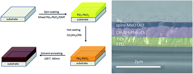
In this work, PbCl2 is used as an additive to assist organolead trihalide perovskite film formation in a two-step sequential deposition process. PbCl2 inhibits PbI2 crystallization and contributes to the full conversion of PbI2 and enhanced perovskite film morphology control. Cl− incorporation into the perovskite improves charge transport within the film, as confirmed by the resulting prolonged photoluminescence lifetime observed. A reaction temperature of approximately 50 °C between the PbI2/PbCl2 film and CH3NH3I isopropanol solution is essential for synthesizing high-performance perovskite solar cells. Addition of PbCl2 results in a perovskite solar cell energy efficiency of 14% and achieves an average efficiency enhancement of approximately 30% compared with that obtained from the control group.
Two-step sequential deposition of perovskite has also been used to fabricate planar heterojunction devices. This technique features improved control of the perovskite film morphology. Two-step sequential deposition of (RNH3)2(CH3NH3)n−1MnI3n+1 (R = butyl, phenethyl; M = Pb, Sn) perovskite film was first reported by Mitzi et al.9 and successfully developed by Grätzel et al.10 for CH3NH3PbI3 synthesis. This deposition technique was first applied to mesoporous structured devices with a scaffold layer in the early reach stages, such as TiO2 or Al2O3. During two-step deposition, a high-concentration PbI2 solution is first spin-coated onto the substrate and then reacted with CH3NH3I. Two-step sequential deposition can be categorized into two according to the treatment in the second step. Thus, deposition can either be a vapor-assisted solution process (VASP) or a solution-based process that includes dipping10 and interdiffusion11 methods.
VASP was first developed by Yang et al.12 A PbI2 thin film prepared by spin-coating was reacted with CH3NH3I vapor at 150 °C to convert the thin film into perovskite, leading to a PCE of 12.1%. The resulting PCE was further enhanced to 16.8% (ref. 13) by lowering the reaction temperature and CH3NH3I vapor pressure. In this work the beneficial effect of using mixed PbI2/PbCl2 precursor in two step process has also been demonstrated.13 Except that the use of mixed PbI2/PbBr2 precursor solution for a sequential deposition process has also been demonstrated.14 Compared with VASP, the second type of deposition solution process is easier to operate and considerably more accessible to diverse perovskite devices. However, the good crystallinity of PbI2 produces undesirable effects. The PbI2 crystal size is confined by the space between nanoparticles in the mesoporous structure but preferably forms large crystals in the planar heterojunction structure. Considering that the second reaction with CH3NH3I is a heterogeneous reaction, large PbI2 crystals will feature reduced accessibility to small organic molecules, thereby resulting in incomplete PbI2 conversion. This phenomenon can severely impact device efficiency and reproducibility. Additionally, variations in PbI2 crystal size lead to changes in the perovskite crystal size, which probably contributes to uncontrollable film morphologies. When N,N-dimethylformamide (DMF) solvent is replaced with dimethyl sulfoxide (DMSO), the molecules of which have stronger coordination with Pb2+ than DMF, PbI2 crystallization can be effectively inhibited, leading to full conversion of PbI2.15 Consequently, high-efficiency CH3NH3PbI3 perovskite solar cells with enhanced reproducibility are obtained.
To the best of our knowledge, the use of Cl− as a dopant agent can result in formation of CH3NH3PbI3−xClx and greatly improve the transport properties of perovskite, especially its hole/electron diffusion length. Cl− can also induce lattice distortion during perovskite crystallization, which slows down the crystal growth rate.16 This phenomenon is mainly inferred from the longer annealing time and higher annealing temperature required for full conversion into perovskite compared with pure PbI2-based materials. In this work, we presented PbCl2 as an additive and adopted interdiffusion of spun stacking layers of PbCl2/PbI2 and CH3NH3I to fabricate perovskite solar cells.11 The PbCl2 additive effectively inhibited crystallization of PbI2 to complete its conversion of PbI2 and controlled the resulting CH3NH3PbI3−xClx film morphology. Introduction of PbCl2 dramatically prolonged the fluorescence lifetime of perovskite, indicating improved charge transport properties within the perovskite layer. The system with PbCl2 additive was more sensitive to the spin-coating temperature of the CH3NH3I/isopropanol solution than that without the additive. Higher temperatures benefited formation of larger perovskite crystal sizes, which remarkably enhanced fill factor (FF) and Jsc. Adjusting the amount of PbCl2 and further optimizing the spin-coating temperature resulted in enhancements in the average PCE of the corresponding perovskite solar cells by over 30% compared with that of pure PbI2-based devices.
We found that the temperature of the FTO substrate and PbI2–PbCl2/DMF solution influenced the final morphology of the perovskite film during spin-coating of the PbI2–PbCl2/DMF solution. Fig. S1† shows a scanning electron micrograph of the film spin-coated from PbI2–PbCl2/DMF solution with 33% molar ratio of PbCl2 at room temperature and then annealed at 100 °C for 60 min. The morphology of this film remarkably differed from that of the film spin-coated at higher temperatures (70 °C; Fig. S1b†). Lower temperatures induced the formation of smaller crystal sizes and higher porosity, which are not beneficial to the morphological control of the perovskite film. Warmer substrates and precursors may contribute to PbI2 crystallization, consistent with other reports that adopted a temperature of 70 °C to spin-coat PbI2/DMF solution during the two-step sequential deposition process.8,17 The morphologies of PbI2/PbCl2 films with varied molar ratios of PbCl2, which are shown in Fig. S2a–c,† are clearly distinguishable from those of pure PbI2 film, which is composed of large flaky crystals, as illustrated in Fig. S2d.† Addition of PbCl2 apparently changed the film morphology by diminishing the PbI2/PbCl2 crystal size and smoothing the film surface to decrease roughness. When the molar ratio was further increased to 50%, film coverage decreased and porosity evidently increased. Well-regulated PbI2/PbCl2 films generally favor the formation of high-quality perovskite film.8,17 Therefore, addition of an appropriate molar ratio of PbCl2 is necessary for morphological control of subsequent perovskite film.
When the amount of PbCl2 added was increased from 0% to 50%, the color of the prepared PbI2/PbCl2 film on prepared substrate changed from yellow to white (Fig. S3†). This change was further demonstrated by the UV-vis absorption spectra of PbI2/PbCl2 films on substrate with different molar ratios of PbCl2. The pure PbI2-based film revealed an absorption peak centered at 500 nm (Fig. 2a), which is attributed to the band-gap excitation of crystallized PbI2. The absorption intensity of the characteristic peak weakened with increasing amount of added PbCl2. The absorption peak at 500 nm disappeared at 50% PbCl2 molar ratio. This phenomenon basically proves the amorphous nature of PbI2. XRD patterns of the PbI2/PbCl2 films (Fig. 2b) also verified the inhibition effect of PbCl2 on PbI2 crystallization. PbI2 films exhibited a strong diffraction peak at 2θ = 12.6°, which corresponds to the (001) crystal plane of crystallized PbI2. The intensity of this characteristic peak significantly decreased when PbCl2 was introduced to the system and completely disappeared in the XRD pattern of PbI2/PbCl2 film when the PbCl2 molar ratio was increased to 50%. The absence of this characteristic diffraction peak indicates that the film is in an amorphous state. The inhibitory effect of PbCl2 may be ascribed to the formation of a new phase (PbClI) which can be identified by XRD pattern of the film. By comparing the XRD of FTO/cTiO2/PbI2:PbCl2 and FTO/cTiO2 (Fig. 2c), we can found that peaks 2θ = 26.4°, 37.8°, 51.4° belongs to the substrate of FTO/cTiO2. And according to previous report13,18 relatively weak peaks at 21.34°, 28.9°, 30.7°, and 34.1°, corresponding to the (120), (121), (211), and (310) crystal planes of PbClI(Fig. 2c). The new double peaks at 2θ = 23.6° and 24.0° also appeared at the XRD pattern of PbI2/PbCl2 based on other PbCl2 of other molar ratios which we believe might be assign to the intermediate phase of PbCl2/PbI2 formed during preparation process. Taken together, the UV-vis absorption spectra and XRD patterns confirm the inhibitory effects of PbCl2 on PbI2 crystallization; such inhibition may accelerate the reaction between PbI2/PbCl2 film and organic CH3NH3I molecules.16
We compared the evolutional processes of the XRD patterns of perovskite films based on PbI2/PbCl2 (33% molar ratio of PbCl2) (Fig. 2d) and pure PbI2-based (Fig. S4†) films at different annealing times. The perovskite peak intensity was fairly weak immediately after spin-coating, especially in the pure PbI2-based sample. This finding suggests that both pure PbI2 and PbI2/PbCl2 films without annealing cannot completely react; such a phenomenon is supported by the scanning electron micrograph showing unreacted PbI2/PbCl2 phase in Fig. S5.† After annealing at 100 °C for 15 min, the pure PbI2 sample still showed diffraction peaks at 2θ = 12.6°, indicating residual unreacted PbI2. The peak intensity of PbI2 continued to decrease until an annealing time of 30 min. The small PbI2 peak was maintained even after 60 min, thereby implying incomplete conversion of PbI2. In the PbI2/PbCl2 samples, the small PbI2 peak disappeared immediately after spin-coating, and the intensity of the perovskite film remained nearly unchanged after 15 min; no characteristic peak of PbI2 was observed at 2θ = 12.6°. The peak of the PbClI phase completely disappeared, likely because of reaction between PbClI phase and MAI that convert into perovskite. These findings indicate that addition of PbCl2 facilitates the reaction between PbI2 and CH3NH3I.
PbCl2 inhibited PbI2 crystallization and assisted in the completion of the PbI2 reaction. Hence, we supposed that addition of PbCl2 may play an important role in perovskite formation and device performance. Thus, we examined the property of perovskite films based on PbI2/PbCl2 films with varying amounts of PbCl2. We found that all of the PbI2/PbCl2 films formed perovskite after solvent annealing treatment. Fig. 3a–d show the scanning electron micrographs of perovskite based on PbI2/PbCl2 films of different molar ratios. The resulting perovskite demonstrated larger crystal sizes and enhanced smoothness compared with the thermally annealed sample as a result of the solvent annealing process (Fig. S6†). The morphology of the perovskite films showed no distinct difference, probably because of solvent annealing. When the added amount of PbCl2 was excessively high or no PbCl2 was added, the grain size and smoothness decreased to a certain extent, likely because of morphological differences in the PbI2/PbCl2 films discussed above.1,2,13 The XRD patterns of the perovskite films (Fig. 4e) formed from PbI2/PbCl2 films of different PbCl2 molar ratios showed peaks at 2θ = 14.08°, 28.5°, 31.8°, and 43.2°, respectively corresponding to the (110), (220), (310), and (330) crystal planes of perovskite. No apparent differences were found between the peak positions of CH3NH3PbI3−xClx and CH3NH3PbI3, in agreement with other reports.13,19
EDS (Energy Dispersive X-ray Spectrometer) results show that CH3NH3PbI3−xClx also exhibits no detection signal of Cl because of content of Cl below the LOD (limit of detection which is about 1% atomic percentage) of EDS (Fig. S7†).17,20,21 According the previous report that the measurement result delivered by XPS (X-ray photoelectron spectroscopy) of Cl atomic percentage in CH3NH3PbI3−xClx-based perovskite is about 0.7%.17,21 Compared with the XRD patterns of perovskite films based on PbI2/PbCl2 films with different molar ratios (Fig. 4e), the pure PbI2-based perovskite film showed the residual characteristic peak of PbI2 at 2θ = 12.6°, indicating incomplete conversion of PbI2. When PbCl2 was introduced to the system, new diffraction peak at 2θ = 15.5° appeared. According to the previous work,19,22,23 this diffraction peak corresponds to the CH3NH3PbCl3 phase with clear identification, and this which also appears in other CH3NH3PbI3−xClx-based perovskite XRD patterns.5,13,17,23 When the amount of added PbCl2 was increased, the characteristic peak intensity of CH3NH3PbCl3 was enhanced. At 50% PbCl2, an obvious peak at 2θ = 15.5° appeared in the XRD pattern (Fig. 4e). The scanning electron micrographs and XRD patterns prove that PbI2/PbCl2 films with different PbCl2 molar ratios could form perovskite films. Excessively high or too low PbCl2 molar ratios resulted in decreased grain sizes and smoothness. Addition of PbCl2 also led to the formation of the CH3NH3PbCl3 phase.
We investigated the photovoltaic parameters of solar cells based on different PbCl2 molar ratios, and the results are summarized in Table 1 and Fig. 4; statistical data derived from 40 devices are listed under each condition. Addition of PbCl2 showed no apparent influence on the open-circuit voltage, which was approximately 1 V. When the amount of PbCl2 added was at a certain range (PbCl2 molar ratio from 0% to 33%), Jsc was not evidently affected. Jsc declined distinctly only when the molar ratio of PbCl2 reached 50%. This phenomenon may have been caused by incomplete conversion of PbCl2. The reaction between PbCl2 and CH3NH3I usually requires longer reaction time and higher reaction temperatures compared with that of PbI2.2,24 However, the reaction time and temperature were limited during the spin-coating process. The amount of CH3NH3I left over on top of the PbI2/PbCl2 film after spin-coating was also limited. These characteristics led to incomplete conversion of PbCl2. The observed phenomena could also be supported by the fact that the optimized reaction temperature for PbI2/PbCl2-based devices is higher than that of pure PbI2-based ones. Addition of PbCl2 evidently improved FF and contributed to the enhancement of PCE. The cells presented the highest average PCE at a PbCl2 molar ratio of 33%. The devices demonstrated the following characteristics: average Voc, 0.98 ± 0.02 V; Jsc, 20.70 ± 1.00 mA cm−2; FF, 0.59 ± 0.03; and PCE, 12.1% ± 0.98%. The average PCE of the devices obtained was enhanced by 30%, from 9.3% to 12.1%, compared with that of the control group.
| PbCl2 molar ratio (%) | Voc (V) | Jsc (mA cm−2) | FF | PCE (%) |
|---|---|---|---|---|
| a Under each condition, the listed result is the standard deviation calculated from 40 devices. | ||||
| 0 | 0.96 ± 0.03 | 20.1 ± 1.33 | 0.48 ± 0.03 | 9.3 ± 0.78 |
| 25 | 1.01 ± 0.02 | 20.3 ± 0.84 | 0.57 ± 0.03 | 11.7 ± 0.90 |
| 33 | 0.98 ± 0.02 | 20.7 ± 1.00 | 0.59 ± 0.03 | 12.1 ± 0.98 |
| 50 | 1.00 ± 0.03 | 18.1 ± 1.21 | 0.53 ± 0.03 | 9.7 ± 0.92 |
We performed time-resolved photoluminescence (PL) measurements on the different perovskite films to explore the mechanism by which PbCl2 affects device performance. Time-resolved PL measurements provide important information on the lifetime of the excited species in the photoactive layer, which can be used to deduce the diffusion length of the charge carriers. All of the test samples adopted the structure of glass/CH3NH3PbI3 or glass/CH3NH3PbI3−xClx. The decay plots obtained are shown in Fig. 3f. All the testing results fit the biexponential decay dynamics, and the fitted parameters are presented in Table S2.† Biexponential decay maybe attributed to variations in the perovskite grain size.17 Slower decay time represent longer diffusion lengths, indicating higher charge collection efficiencies. Addition of PbCl2 effectively prolonged the PL lifetime τslow. At a PbCl2 molar ratio of 33%, the lifetime τslow reached 172.63 ns, which is far longer than the 75.17 ns of τslow of the pure PbI2-based sample. A PbCl2 molar ratio higher than 33% decreased the lifetime. This variation in the PL lifetime basically agrees with the variation in device performance. Lifetime extension can be explained by Cl− doping, which has been reported to remarkably improve transport property.16,25 Thus, addition of PbCl2 can enhance device performance by improving perovskite film transport properties.
The spin-coating temperature of the CH3NH3I/isopropanol solution plays an important role in device efficiency during device fabrication, especially when PbI2/PbCl2-based devices are produced. This sensitivity to temperature may be derived from the fact that PbCl2 requires higher reaction temperature and longer reaction time to convert into perovskite.2,24 Excess Cl− may sublime in the form of CH3NH3Cl and leave only trace amounts of chloride in the perovskite. The sublimation process would therefore influence the phase transformation process, wherein lattice distortion caused by Cl− doping and exclusion of organic molecules could improve perovskite crystallization5,12,26,27. Fig. 5e shows the XRD patterns of CH3NH3PbI3−xClx prepared at different temperatures. When the spin-coating temperature was enhanced from 30 °C to 60 °C, the peak intensity of the formed perovskite was reinforced and the half-peak width of the characteristic peak at 2θ = 14.08° became smaller, indicating improved perovskite crystallinity. The characteristics of the perovskite films prepared at different temperatures shown in Fig. 5a–d indicate that larger crystalline grains are preferred at higher temperatures, further supporting the enhancement of perovskite crystallization. Compared with the XRD patterns of perovskite films at spin-coating temperatures of 30 °C (Fig. S8†) and 50 °C (Fig. 2d), the intensity of the characteristic perovskite peak at 2θ = 14.08° obtained immediately after 50 °C hot casting without annealing was much stronger than that observed at 30 °C. This phenomenon suggests that larger amounts of PbI2/PbCl2 convert into the perovskite phase before annealing treatment. Higher conversion ratios of PbI2/PbCl2 may benefit the formation of larger perovskite grain sizes. When the hot spin-coating temperature of the CH3NH3I/isopropanol solution reached 60 °C, severe damage of the perovskite film surface is observed (Fig. S9†). This development is mainly due to the restriction of the boiling temperature (82 °C) of isopropanol. High spin-coating temperatures accelerate the evaporation of isopropanol and result in rapid separation of CH3NH3I to form visible crystals. Excessive CH3NH3I residues may also affect device performance. Thus, reaction temperatures of no more than 60 °C may ensures device performance.
The photovoltaic parameters of 40 devices for each spin-coating temperature are shown in Fig. S10.† No apparent difference in Voc was observed under the different spin-coating temperatures, and values of approximately 1 V were consistently obtained. The different spinning temperatures mainly affected the Jsc and FF values of the devices. When the temperature was increased from 30 °C to 50 °C, the average Jsc increased from 16.68 mA cm−2 to 20.65 mA cm−2, and the average FF increased from 0.54 to 0.59. The average Jsc values of devices based on different spin-coating temperatures corresponded to the IPCE integral values at varied spin-coating temperatures (Fig. 6a). This phenomenon can be explained by the formation of larger grain sizes of perovskite at higher temperatures, as confirmed by the XRD patterns and scanning electron micrographs described earlier. Larger grain sizes of perovskite decrease the impact of grain boundaries on charge separation and transmission. Grain boundaries, especially those on the longitudinal transport pathway, induce charge recombination, which severely affected the device performance.11 Fewer grain boundaries provide effective charge transport, inhibit interface charge recombination, and improve Jsc and FF. When the temperature was excessively high, CH3NH3I precipitated before reacting with PbI2/PbCl2 during spin-coating, and the residual CH3NH3I negatively affected device performance. The optimized spin-coating temperature was 50 °C, at which point the average PCE was enhanced by 34% compared with that at 30 °C. The best device achieved a maximum PCE of 14% as well as Voc, Jsc, and FF values of 0.99 V, 21.8 mA cm−2, and 0.64, respectively (Fig. 6d).
We further compared the device performances of pure PbI2 with the PbI2/PbCl2 system obtained at different CH3NH3I isopropanol solution spin-coating temperatures (Fig. S11†). Similar to PbI2/PbCl2, the Voc of the devices showed no apparent difference under various spin-coating temperatures. However, the Jsc of the PbI2-based device was not sensitive to the temperature, and the average Jsc was approximately 20 mA cm−2, as shown in Fig. 6b. The influence of temperature was mainly observed in terms of FF. The optimal spin-coating temperature of the pure-PbI2 device was 40 °C, which is lower than that of the PbI2/PbCl2-based device (Fig. 6c), and the distribution of the PCE of the former was wider compared with that of the latter. Under optimized fabrication conditions, the average PCE based on PbI2/PbCl2 was enhanced by 21% compared with that of the control group.
Photocurrent hysteresis is one of the major issues hindering accurate measurement of device efficiency, especially for planar heterojunction devices, which often present obvious hysteresis.28 We found that both PbI2/PbCl2 and PbI2-based device show a certain degree of hysteresis. The reverse scanning efficiency was higher than the forward scanning efficiency, and the scanning rate impacted hysteresis. Fig. S12† shows that the device demonstrates the smallest hysteresis at a scanning rate of 0.1 V s−1. Hysteresis was aggravated when the scanning rate was higher or lower than this value. This phenomenon may be related to the device structure and fabrication process.28 Independent of the PCE of the device, all of the J–V curves presented crosses, which are caused by overestimation of Jsc during forward scanning or underestimation of Jsc during reverse scanning (Fig. S13†). This characteristic may be relevant to the grain size of the perovskite according to a previous report.29 The variation in PCE at 0.1 V s−1 scanning rate was generally within 2%. Thus, this condition was employed in typical characterizations. In order to better evaluate our device performance, we took the steady-state measurements and the results is given in the Fig. S14.† No apparent difference PCE acquired from the steady-state measurement and from J–V plot was found. During the steady-state measurement we found the current fast raised when the device was first exposure to the light and declined about 3.2% during the 180 s measurement process. The decline of the photocurrent might because of the inferior stability under the ambient measurement condition.
In summary, PbCl2 is an effective additive for organolead trihalide perovskite thin films. PbCl2 inhibited crystallization of PbI2, resulting in complete conversion of PbI2 and improvement of the perovskite morphology. Addition of PbCl2 resulted in the formation of CH3NH3PbI3−xClx and remarkably prolonged the photoluminescence lifetime, which implies enhancements in transport property. A suitable spin-coating temperature enabled enlargement of the perovskite grain size, thereby enhancing both FF and Jsc, which are crucial for high-efficiency devices. Thus, addition of PbCl2 to the PbI2 DMF precursor solution is a simple and potent method to achieve highly efficient heterojunction perovskite solar cells.
Footnote |
| † Electronic supplementary information (ESI) available. See DOI: 10.1039/c5ra23062d |
| This journal is © The Royal Society of Chemistry 2016 |