Energetic stability, STM fingerprints and electronic transport properties of defects in graphene and silicene

Soumyajyoti Haldara, Rodrigo G. Amorim*ab, Biplab Sanyala, Ralph H. Scheichera and Alexandre R. Rochac
aDivision of Materials Theory, Department of Physics and Astronomy, Uppsala University, Box-516, SE 75120, Sweden
bDepartamento de Física, ICEx, Universidade Federal Fluminense, Volta Redonda, RJ, Brazil. E-mail: rgamorim@id.uff.br
cInstituto de Física Teórica, Universidade Estadual Paulista Júlio de Mesquita Filho – UNESP, São Paulo, Brazil

Received 2nd November 2015 , Accepted 4th January 2016

First published on 7th January 2016


Abstract

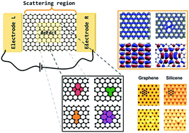
Novel two-dimensional materials such as graphene and silicene have been heralded as possibly revolutionary in future nanoelectronics. High mobilities, and in the case of silicene, its seemingly natural integration with current electronics could make them the materials of next-generation devices. Defects in these systems, however, are unavoidable particularly in large-scale fabrication. Here we combine density functional theory and the non-equilibrium Green's function method to simulate the structural, electronic and transport properties of different defects in graphene and silicene. We show that defects are much more easily formed in silicene, compared to graphene. We also show that, although qualitatively similar, the effects of different defects occur closer to the Dirac point in silicene, and identifying them using scanning tunneling microscopy is more difficult particularly due to buckling. This could be overcome by performing direct source/drain measurements. Finally we show that the presence of defects leads to an increase in local current from which it follows that they not only contribute to scattering, but are also a source of heating.

1 Introduction

Graphene1 – a single layer of carbon atoms arranged in a honeycomb lattice – was first synthesized in 2004, and since then has spun a whole new era of research in two-dimensional materials.2,3 It has the potential for a wide range of applications due to its interesting electronic and structural properties.1,4–8 At the same time, the recent theoretical proposal of silicon's counter part to graphene, silicene9 and its experimental synthesis10,11 could be a viable option for a smooth integration with current semiconductor technology. The hexagonal structure and electronic properties are similar to graphene – including the so-called Dirac cone. For instance its mobility is in the same order of magnitude12 with the added bonus that it is made of the same material as current electronic devices.

First experiments reporting evidence of silicene were made on deposited metallic substrates.10,11 Furthermore, silicene has a high reactivity when exposed to air. These were the hindering issues for further development of silicene-based electronic devices. Recent advances have allowed for the fabrication of encapsulated sheets, which behave in a similar fashion to suspended monolayer silicene, and possibly solve the reactivity problem.13,14 Nonetheless, for large-scale fabrication of both graphene and silicene, most synthesis processes such as CVD lead to some degree of defects.15,16 Even if improvements in fabrication are made, it is highly unlikely that one will be able to obtain a perfectly defect-free monolayer, be it silicene or graphene.

Theoretical predictions of defects in graphene17,18 and also silicene19 have been studied from electronic structure point of view. There are significant contributions concerning creation,20 mobility,21 self healing,22 and also electronic structure of defects using different methods,21–23 particularly for graphene. However, we note that there is a missing point in the understanding of electronic transport properties of defects in two-dimensional silicene and also on graphene. Most of the works focus in model Hamiltonians,24 and, most importantly, they target typically nanoribbons.25 Here, we investigated fully 2D systems for graphene and silicene, and the defects' influence on the electronic transport properties without edge effects present in nanoribbons.

On the one hand, defects are usually seen as detrimental to device properties,15 but in some cases, especially at the nanoscale, defects can bring about new beneficial effects which could be utilized for applications.26–30 There have been extensive reports about the effects on the electronic structure of graphene in the presence of defects.,17,31–33 but considerably less so for the case of silicene.21 No systematic study has yet been presented on the effect in transport properties due to the most important defects in both graphene and silicene, particularly in terms of local effects.

In that sense, it is important to determine the effects of the most stable defects on the electronic transport properties of these two-dimensional systems. In order to address the possibility of employing either graphene or silicene as candidates for nanodevices,34 we combined ab initio density functional theory (DFT)35,36 with the non-equilibrium Green's function (NEGF)37,38 method to perform electronic transport calculations. Different defects were analyzed and compared between the two monolayers. We show that the formation of defects is more likely in silicene, compared to graphene. Nonetheless, qualitatively, they give rise to similar transport fingerprints with respect to resonances associated with defect levels. Furthermore, the presence of defects leads to a significant enhancement of local currents, which can be a source of heating, as well as degraded performance.

2 Methodology

Fig. 1 shows the setup used in the different parts of the simulations. In our calculations, we considered graphene (GR), and hexagonal silicene (h-Si). In all cases we considered a fully periodic system in order to mimic the two-dimensional system. Differently from nanoribbons, no edge effects are expected. For each case, five configurations were explored, namely the pristine case, a Stone–Wales defect (SW), a monovacancy (1V), and two types of divacancies: one with two pentagons and one octagon (2V-585), and another with three pentagons and three heptagons (2V-555777). In graphene these are known to be the most likely defects.39,40 The different defect arrangements are highlighted in Fig. 1a–d. From a top view the defects look similar for both GR and h-Si.
image file: c5ra23052g-f1.tif
Fig. 1 Top view of the schematic representation of the defective structures used in this work for both graphene and silicene: (a) Stone–Wales (SW), (b) monovacancy (1V), (c) divacancy (2V-585) and (d) divacancy (2V-555777). Side view of (e) graphene, (f) silicene. While pristine graphene is perfectly flat, silicene exhibits a rugged structure. (g) Setup used in the electronic transport calculations for both graphene and silicene: two electrodes and a central scattering region.

The calculations were performed using a double-ζ polarized basis set (DZP) for valence electrons, and norm-conserving pseudopotentials.41 We used an orthorhombic unit cell of 21.56 × 15.00 × 29.88 Å (34.20 × 15.0 × 47.4 Å) for graphene (silicene), and the z direction (Lz), labeled scattering region in Fig. 1g (the monolayer lies in the xz plane). A vacuum region of 15.00 Å was used in the y direction to avoid spurious interaction with the periodic images. We performed supercell size tests to avoid interaction between the mirror images in the zx plane, and for distances larger than 10 Å the defect–defect interaction effects are negligible, owing to the electronic properties convergence. For the relaxation of the defect, we used the Monkhorst–Pack scheme with a k-points grid of 6 × 1 × 4, and for electronic transport 24 × 1 × 1 k-points for k-space integration.

The generalized gradient approximation as proposed by Perdew, Burke and Ernzerhof42 (PBE-GGA) for the exchange–correlation functional was employed. In all cases, the conjugate gradient (CG) method was applied to obtain equilibrium structures with residual forces on each atomic component no greater than 0.01 eV Å−1.

From the local density of states (LDOS), it is possible to simulate scanning tunneling microscopy images (STM). For this purpose, we employed the Tersoff–Hamann43 approximation, where the STM tip is considered to be of s-orbital type, and the tunneling current is proportional to the LDOS. In the linear regime dI/dV ∝ LDOS. Within this approach one sums over all Kohn–Sham states of the system in the energy window {EF, EF ± V}, where V is the applied bias, and EF is the Fermi energy. The isosurfaces of the LDOS can be associated with empty (filled) states for positive (negative) values of V at a constant height. All calculations were performed using the SIESTA44 code.

For the transport calculations, we initially follow the proposal by Caroli et al.;46 the system of interest is split into three segments, namely, a scattering region consisting of either GR or h-Si with a defect, and two semi-infinite electrodes (left and right) taken here to be the pristine system. A representation of a defect free system is shown in Fig. 1g as an example. In all cases transport occurs along the z direction, and we considered translational invariance in the x direction. We ensure that the charge density at the edges of the box along z matches the one from bulk GR (h-Si) for consistency of the methodology. Using localized basis sets, it is possible to write the k-dependent retarded Green's functions for the scattering region as:

image file: c5ra23052g-t1.tif
where SS and HS are the overlap matrix and Hamiltonian for the scattering region, respectively, and ΣL/R are self-energies that take into account the effect from the left (L) and right (R) electrodes onto the central region. In our case the Hamiltonian used is the Kohn–Sham Hamiltonian, and we employed the TranSiesta package37 with the same DFT convergence parameters as used in the SIESTA calculations.

The charge density is self-consistently calculated via Green's functions until convergence is achieved. From this, we can obtain the transmission coefficient as:

 
image file: c5ra23052g-t2.tif(1)
where Γα(E, kx) = i[Σα(E, kx) − Σα(E, kx)], with α ≡ {L, R}, and the total transmission is given by
 
image file: c5ra23052g-t3.tif(2)
where ωkx is the weight given to each k-point. Further details regarding the methods for calculating electronic transport properties can be found in the literature.37,38

Finally, one can also go back to the general definition of the current in the Keldysh formalism, and obtain the current density between two sites M and N as:

 
image file: c5ra23052g-t4.tif(3)
where the sum is performed over all localized atomic orbitals n and m of the basis set, which are associated with sites N and M, respectively. This way it is possible to determine the current pathways.

3 Results

The obtained relaxed lattice constants in our calculations were 2.49 Å (3.95 Å) for graphene (silicene). The defect concentration for graphene (silicene) is 0.00155 (0.000617) defects per Å2. Most importantly the average distance between defects is 25.4 Å (40.24 Å). Compared with experiments47 one finds that, in our simulations, the defect distance is ∼3 times larger. Our benchmark calculations with different cell sizes (not shown here) indicates that the electronic properties (the density of states) have converged. Fig. 1e and f show graphene (silicene) side view structures, where one can note that silicene is buckled (by 0.46 Å in the out-of-plane direction) while graphene is planar. We also performed calculations on planar silicene, but the buckled structure is 0.1 eV per atom more stable than the planar one.9,34

We then investigated the stability of all defects. In order to characterize the systems with different number of atoms, we considered the formation energy,

 
Ef = EDtotalEtotal + i, (4)
where EDtotal (system + defect) is the total energy of the defective system, Etotal is the total energy of the pristine system, N is the number of removed atoms, and μi is the chemical potential (i = C or Si). We assumed as a source of carbon and silicon the respective pristine monolayers.

Table 1 lists the defect formation energies in graphene and in silicene. First we note that, for any given defect, silicene exhibits a smaller Ef than graphene. In fact, the formation energies for h-Si are smaller than those of GR by at least a factor of 2. This can be understood in terms of the cohesive energy; for graphene, the cohesive energy found was 8.21 eV per atom, while for silicene, 4.27 eV per atom. These results indicate that it is easier to remove atoms from the latter, and thus one would expect the existence of defects to be more likely in silicene than in graphene. Furthermore the hierarchy of Ef for GR is given by SW < 2V-555777 < 2V-585 < 1V, whereas for h-Si a slightly different order of stability was observed, namely SW < 2V-555777 < 1V < 2V-585. Our results are consistent with the results obtained by Amorim et al.39 for graphene, and by Gao et al.21 for silicene. The 2V-585 defect is less stable than 2V-55577 in graphene due to two broken bonds, as it has been demonstrated in a previous work.39 The same argument is valid for silicene. On the other hand, the formation energy of the single vacancy (1V) is smaller with respect to the 2V-585 in silicene compared to graphene. This is due to the buckling of the h-Si structure, which allows for a better accommodation of the dangling bonds. This is also highlighted by the lack of a magnetic moment when compared to the 1.4 μB observed in graphene.

Table 1 Defect formation energies in graphene and silicene
Defect Formation energy (eV)
Graphene Silicene
SW 4.87 1.84
1V 7.62 2.87
2V-555777 6.63 2.74
2V-585 7.48 3.24


We turn our discussion now to a comparative analysis of the defect fingerprints in graphene and silicene as they can be observed in the simulated STM images presented here. Fig. 2 shows simulated STM images for graphene (silicene) on the left (right) hand-side panel for filled states with an applied bias of −1.0 V. While for the pristine graphene case (Fig. 2a), it is easily possible to identify the hexagonal rings because all carbon atoms are in the same plane, the hexagonal lattice for pristine silicene forms a buckled structure,9,34 thus the bright spots in the STM images shown in Fig. 2a for pristine silicene are atoms from only one of the two sublattices, namely the one that is positioned closer to the simulated STM tip.


image file: c5ra23052g-f2.tif
Fig. 2 Simulated STM images for filled states with applied bias of −1.0 V for the different defects in (1) graphene and (2) silicene. (a) Pristine structure with hexagonal atomic configurations overlayed, (b) Stone–Wales defect, (c) single vacancy, (d) 2V-585 divacancy, and (e) 2V-555777 divacancy. The STM images were generated using the Tersoff–Hamann approach with WSxM software.45

For the Stone–Wales defect in graphene it is possible to identify the pentagon's rings in Fig. 2b and also two bright spots (upper and lower part of the image) residing on one atom from each heptagon edge. For the SW defect in silicene, the STM image is more complicated to analyze due to the buckling. As the defect atoms are in different planes, it becomes difficult to recognize the defect. Despite this difficulty, we can recognize the heptagons as two large holes in the figure and also there are two spots from the pentagons that lie in the same plane. The monovacancy in graphene has three dangling bonds due to one missing atom when the defect is formed; one of them moves up forming a very bright spot (Fig. 2c) and the other two dangling bonds move close to each other. For silicene an opposite trend is seen: two dangling bonds are displaced slightly down causing two bright spots for the first two neighbors. In this case the defect is tilted and the pentagon is darkened.

The divacancy 2V-585 is shown in Fig. 2d, and we clearly note two pentagons above and below the void. In the silicene case (Fig. 2d), there are two atoms of the upper pentagon that are displaced upward compared to their neighbors, and they appear bright in the image. At the same time, two atoms from the lower pentagon are displaced downwards and because of that they are not visible. Finally, for the 2V-555777 defect in graphene, the three pentagons are very easy to identify due to their brightness. For silicene (Fig. 2e), we note three larger holes that represent the heptagon centers and also one atom of each pentagon is higher compared to their nearest neighbors. These three pentagons are also easy to identify with the STM images.

Overall, we note that the buckling leads to a smoother charge density in silicene in the defect region. This means one would expect it to be a more difficult task to identify these defects in silicene21 using STM. More importantly, in an encapsulated system such as those recently reported,13,14 STM images of the defects would be inaccessible. One alternative way to probe the defects is to calculate the transverse electronic transport properties of the monolayers. In principle, one can look for signatures of the different defects such as resonances that could be observed by applying a combination of source/drain and gate voltages. Fig. 3 shows the transmission coefficients for different defects in both GR and h-Si. In the pristine case, one notes the Dirac cone shape in the transmittance for both cases as expected. In principle, the transport properties are similar, but for the same energy the transmittance is larger for silicene, as the valence and conduction bands are notably narrower compared to graphene.9,48 Analyzing the transport properties of graphene (presented in Fig. 3a) for the energy range below the Fermi level, the SW and the 2V-585 defects do not exhibit considerable changes compared to the pristine case apart from a small decrease in the slope of the curve. For energies down to about −0.4 eV the same can be said about the monovacancy. For lower energies, however, one notices a broad resonance centered at −0.8 eV. The most significant changes are observed for the 2V-555777 defect; there is a strong suppression of the transmission, which can be associated to the scattering at a state located at the reconstructed divacancy site. At positive energies, the main effect is the change in the slope of the transmission curve except for a sharp resonance at around 0.65 eV for the SW defect.


image file: c5ra23052g-f3.tif
Fig. 3 Transmission coefficients as a function of energy for the different defects in (a) graphene, and (b) silicene. The insets show a zoom-in of the region around the Dirac cone.

For silicene, the qualitative behaviour is somewhat similar, the main difference comes from the fact that the resonances appear closer to the Fermi level for both positive and negative energies. Other resonances at higher energies become evident as well. These would be higher/lower in energy in graphene. Thus, by applying a small bias and a relatively small gate voltage one could access these resonances, and by comparing the relative behaviour, differentiate between the defects. The key point is that the different defects present resonances at different energies, thus sweeping the gate voltage would allow access to their signal in the IV characteristics.

Here, it is important to stress that our results are performed for 2D graphene (silicene), without border effects. One significant difference is the lack of spin polarization on the edges, a signature of specific directions in nanoribbons. Comparing our results with those of 1D silicene presented by Zha25 et al. we notice significant differences. The resonance due to the Stone–Wales defect in their case is located at the Fermi level, whereas in our results there is a resonance approximately at 0.4 eV above the Fermi level. This is a consequence of the fact that in a nanoribbon only a single conductance channel is present whereas in two-dimensional silicene a Dirac cone is present with a large number of channels along kx.

Finally, we look at the effects of these resonances on the local transport properties.49 We present results for the pristine and the SW defect as they show resonances. Fig. 4 shows the local current density for these systems. For graphene (EEF = +0.65 eV) and h-Si (EEF = +0.29 eV), the respective energy chosen corresponds to the resonance position of each system. Analyzing both pristine systems we note that the current flows from the left side to the right side following a zigzag path as expected. Due to the symmetry of the system, the current flowing upwards is identical to the one going downwards and its net effect is zero (see Fig. 4a). The wave function (WF) is shown in Fig. 4b, where blue represents the real part and the imaginary is colored in red. We note similar behavior for the pristine case, the WF is spread throughout the whole system, and is not localized at specific sites, following the same behavior. For the SW defect we note, for both graphene and silicene, a concentration of local current in the vicinity of the defect. This is consistent with a Fano resonance, where one has a bound state weakly coupled to the continuum of the band (the pristine system). This localized state can be seen in Fig. 4d. As a consequence, the lifetime of the electron in this region is longer and the local current is much higher. In essence we note that the resonances give rise to regions of high current density (and also higher resistance), thus areas where one might expect local heating that can be detrimental for device functioning. It is important to remark that the direction of the local current depends on the position of source and drain with respect to the orientation of the sheet, however the total current should not exhibit such a dependence, as we have a Dirac cone, and the band structure is isotropic for energies around the Fermi level. Furthermore, the WF is not direction dependent. Thus the local heating should be similar for transport along either the zigzag (z) or the armchair (x) direction.


image file: c5ra23052g-f4.tif
Fig. 4 Top view of local current (LC) and wave functions (WF) for both graphene and silicene: (a) pristine structure (LC); (b) pristine WF; (c) Stone–Wales defect and (d) Stone–Wales (WF). The images presented correspond to a zoomed-in region of the actual simulation cell presented in Fig. 1g.

4 Conclusions

In conclusion, we studied four different defects (SW, 1V, 2V-585 and 2V-555777) in the 2D materials graphene and silicene using density functional theory and the non-equilibrium Green's function method. We investigated these two systems (graphene and silicene) in terms of their structural stability, electronic structure and transport properties. The defects in silicene have smaller formation energies due to its lower cohesion energy and buckled structure. We showed the STM simulated images of each defect using Tersoff–Hamman theory, and the defect fingerprint as a guide for experimentalists to identify these defects. Particularly in silicene this identification process is not as straightforward due to buckling of the structure. We show that this could be overcome by directly measuring the IV characteristics and looking for defect fingerprints. Although we have presented results for a single defect, the average distance between defects considered here is comparable to the ones relevant in experiments.

Finally, the local currents for pristine, and SW defects were discussed. The presence of defects is usually associated with scattering (and decreasing the current). Here we also showed that resonances created by defects lead to increased local current densities, which in turn would result in heating and possible performance degradation.

Acknowledgements

Financial support from the Carl Tryggers Stiftelse and the Swedish Research Council (VR, Grant No. 621-2009-3628) is gratefully acknowledged. S. H. and B. S. would also like to acknowledge KAW foundation for financial support. The Swedish National Infrastructure for Computing (SNIC), the Uppsala Multidisciplinary Center for Advanced Computational Science (UPPMAX) and the PRACE-2IP project (FP7 RI-283493) resource Abel supercomputer based in Norway at University of Oslo provided computing time for this project.

References

  1. K. S. Novoselov, A. K. Geim, S. V. Morozov, D. Jiang, Y. Zhang, S. V. Dubonos, I. V. Grigorieva and A. A. Firsov, Science, 2004, 306, 666–669 CrossRef CAS PubMed .
  2. K. S. Novoselov, D. Jiang, F. Schedin, T. J. Booth, V. V. Khotkevich, S. V. Morozov and A. K. Geim, Proc. Natl. Acad. Sci. U. S. A., 2005, 102, 10451–10453 CrossRef CAS PubMed .
  3. S. Z. Butler, S. M. Hollen, L. Cao, Y. Cui, J. A. Gupta, H. R. Gutiérrez, T. F. Heinz, S. S. Hong, J. Huang, A. F. Ismach, E. Johnston-Halperin, M. Kuno, V. V. Plashnitsa, R. D. Robinson, R. S. Ruoff, S. Salahuddin, J. Shan, L. Shi, M. G. Spencer, M. Terrones, W. Windl and J. E. Goldberger, ACS Nano, 2013, 7, 2898–2926 CrossRef CAS PubMed .
  4. K. Watanabe, T. Taniguchi and H. Kanda, Nat. Mater., 2004, 3, 404–409 CrossRef CAS PubMed .
  5. T. Georgiou, R. Jalil, B. D. Belle, L. Britnell, R. V. Gorbachev, S. V. Morozov, Y.-J. Kim, A. Gholinia, S. J. Haigh, O. Makarovsky, L. Eaves, L. A. Ponomarenko, A. K. Geim, K. S. Novoselov and A. Mishchenko, Nat. Nanotechnol., 2013, 8, 100–103 CrossRef CAS PubMed .
  6. G. T. Feliciano, C. Sanz-Navarro, M. D. Coutinho-Neto, P. Ordejón, R. H. Scheicher and A. R. Rocha, Phys. Rev. Appl., 2015, 3, 034003 CrossRef .
  7. G. L. Lay, Nat. Nanotechnol., 2015, 10, 202–203 CrossRef CAS PubMed .
  8. J. Prasongkit, R. G. Amorim, S. Chakraborty, R. Ahuja, R. H. Scheicher and V. Amornkitbamrung, J. Phys. Chem. C, 2015, 119, 16934–16940 CAS .
  9. S. Cahangirov, M. Topsakal, E. Aktürk, H. Şahin and S. Ciraci, Phys. Rev. Lett., 2009, 102, 236804 CrossRef CAS PubMed .
  10. P. Vogt, P. D. Padova, C. Quaresima, J. Avila and E. Frantzeskakis, Phys. Rev. Lett., 2012, 108, 155501 CrossRef PubMed .
  11. A. Fleurence, R. Friedlein, T. Ozaki, H. Kawai, Y. Wang and Y. Yamada-Takamura, Phys. Rev. Lett., 2012, 108, 245501 CrossRef PubMed .
  12. Z. G. Shao, X. S. Ye, L. Yang and C. L. Wang, J. Appl. Phys., 2013, 114, 2013–2016 Search PubMed .
  13. P. D. Padova, C. Ottaviani, C. Quaresima and B. Olivieri, 2D Mater., 2014, 1, 021003 CrossRef .
  14. L. Tao, E. Cinquanta, D. Chiappe, C. Grazianetti, M. Fanciulli, M. Dubey, A. Molle and D. Akinwande, Nat. Nanotechnol., 2015, 10, 1–5 CrossRef PubMed .
  15. H. S. Song, S. L. Li, H. Miyazaki, S. Sato, K. Hayashi, A. Yamada, N. Yokoyama and K. Tsukagoshi, Sci. Rep., 2012, 2, 1–6 Search PubMed .
  16. T. Niu, M. Zhou, J. Zhang, Y. Feng and W. Chen, J. Am. Chem. Soc., 2013, 135, 8409–8414 CrossRef CAS PubMed .
  17. J. C. Meyer, C. Kisielowski, R. Erni, M. D. Rossell, M. F. Crommie and A. Zettl, Nano Lett., 2008, 8, 3582–3586 CrossRef CAS PubMed .
  18. F. Banhart, J. Kotakoski and A. V. Krasheninnikov, ACS Nano, 2011, 5, 26–41 CrossRef CAS PubMed .
  19. S. Li, Y. Wu, Y. Tu, Y. Wang, T. Jiang, W. Liu and Y. Zhao, Sci. Rep., 2015, 5, 7881 CrossRef PubMed .
  20. A. C. Ferrari, F. Bonaccorso, V. Falko, K. S. Novoselov, S. Roche, P. Bøggild, S. Borini, F. Koppens, V. Palermo, N. Pugno, J. A. Garrido, R. Sordan, A. Bianco, L. Ballerini, M. Prato, E. Lidorikis, J. Kivioja, C. Marinelli, T. Ryhänen, A. Morpurgo, J. N. Coleman, V. Nicolosi, L. Colombo, A. Fert, M. Garcia-Hernandez, A. Bachtold, G. F. Schneider, F. Guinea, C. Dekker, M. Barbone, C. Galiotis, A. Grigorenko, G. Konstantatos, A. Kis, M. Katsnelson, C. W. J. Beenakker, L. Vandersypen, A. Loiseau, V. Morandi, D. Neumaier, E. Treossi, V. Pellegrini, M. Polini, A. Tredicucci, G. M. Williams, B. H. Hong, J. H. Ahn, J. M. Kim, H. Zirath, B. J. van Wees, H. van der Zant, L. Occhipinti, A. Di Matteo, I. A. Kinloch, T. Seyller, E. Quesnel, X. Feng, K. Teo, N. Rupesinghe, P. Hakonen, S. R. T. Neil, Q. Tannock, T. Löfwander and J. Kinaret, Nanoscale, 2014, 7, 4598–4810 RSC .
  21. J. Gao, J. Zhang, H. Liu, Q. Zhang and J. Zhao, Nanoscale, 2013, 5, 9785–9792 RSC .
  22. V. O. Özçelik, H. H. Gurel and S. Ciraci, Phys. Rev. B: Condens. Matter Mater. Phys., 2013, 88, 045440 CrossRef .
  23. A. D. S. Martins and M. Veríssimo-Alves, J. Phys.: Condens. Matter, 2014, 26, 365501 CrossRef PubMed .
  24. K. Shakouri, H. Simchi, M. Esmaeilzadeh, H. Mazidabadi and F. M. Peeters, Phys. Rev. B: Condens. Matter Mater. Phys., 2015, 92, 035413 CrossRef .
  25. D. Zha, C. Chen, J. Wu and M. Wang, Int. J. Mod. Phys. B, 2015, 29, 1550061 CrossRef CAS .
  26. A. R. Rocha, T. B. Martins, A. Fazzio and A. J. R. da Silva, Nanotechnology, 2010, 21, 345202 CrossRef CAS PubMed .
  27. C. Xu, G. Luo, Q. Liu, J. Zheng, Z. Zhang, S. Nagase, Z. Gao and J. Lu, Nanoscale, 2012, 4, 3111 RSC .
  28. H. Liu, J. Gao and J. Zhao, J. Phys. Chem. C, 2013, 117, 10353 CAS .
  29. W.-F. Tsai, C.-Y. Huang, T.-R. Chang, H. Lin, H.-T. Jeng and A. Bansil, Nat. Commun., 2013, 4, 1500 CrossRef PubMed .
  30. Z. Ni, H. Zhong, X. Jiang, R. Quhe, G. Luo, Y. Wang, M. Ye, J. Yang, J. Shi and J. Lu, Nanoscale, 2014, 6, 7609–7618 RSC .
  31. A. Hashimoto, K. Suenaga, A. Gloter, K. Urita and S. Iijima, Nature, 2004, 430, 870–873 CrossRef CAS PubMed .
  32. M. H. Gass, U. Bangert, A. L. Bleloch, P. Wang, R. R. Nair and A. K. Geim, Nat. Nanotechnol., 2008, 3, 676–681 CrossRef CAS PubMed .
  33. D. L. Matz, H. Sojoudi, S. Graham and J. E. Pemberton, J. Phys. Chem. Lett., 2015, 6, 964–969 CrossRef CAS PubMed .
  34. R. G. Amorim and R. H. Scheicher, Nanotechnology, 2015, 26, 154002 CrossRef PubMed .
  35. P. Hohenberg and W. Kohn, Phys. Rev., 1964, 155, 864–870 CrossRef .
  36. W. Kohn and L. J. Sham, Phys. Rev., 1965, 385, 1133–1138 CrossRef .
  37. M. Brandbyge, J.-L. Mozos, P. Ordejón, J. Taylor and K. Stokbro, Phys. Rev. B: Condens. Matter Mater. Phys., 2002, 65, 165401 CrossRef .
  38. A. R. Rocha, V. García-Suárez, S. Bailey, C. Lambert, J. Ferrer and S. Sanvito, Phys. Rev. B: Condens. Matter Mater. Phys., 2006, 73, 85414 CrossRef .
  39. R. G. Amorim, A. Fazzio, A. Antonelli, F. D. Novaes and A. J. R. da Silva, Nano Lett., 2007, 7, 2459–2462 CrossRef CAS PubMed .
  40. J. Padilha, R. Amorim, A. Rocha, A. da Silva and A. Fazzio, Solid State Commun., 2011, 151, 482–486 CrossRef CAS .
  41. N. Troullier, Phys. Rev. B: Condens. Matter Mater. Phys., 1991, 43, 1993–2006 CrossRef CAS .
  42. J. P. Perdew, K. Burke and M. Ernzerhof, Phys. Rev. Lett., 1996, 77, 3865–3868 CrossRef CAS PubMed .
  43. J. Tersoff and D. R. Hamann, Phys. Rev. B: Condens. Matter Mater. Phys., 1985, 31, 805 CrossRef CAS .
  44. M. Soler, E. Artacho, J. D. Gale, A. Garc, J. Junquera, P. Ordej and S. Daniel, J. Phys.: Condens. Matter, 2002, 2745, 2745–2779 CrossRef .
  45. I. Horcas, R. Fernández, J. M. Gómez-Rodríguez, J. Colchero, J. Gómez-Herrero and A. M. Baro, Rev. Sci. Instrum., 2007, 78, 13705 CrossRef CAS PubMed .
  46. C. Caroli, R. Combescot, P. Nozieres and D. Saint-James, J. Phys. C: Solid State Phys., 1971, 4, 916–929 CrossRef .
  47. M. M. Ugeda, I. Brihuega, F. Guinea and J. M. Gómez-Rodríguez, Phys. Rev. Lett., 2010, 104, 096804 CrossRef CAS PubMed .
  48. A. H. Castro Neto, F. Guinea, N. M. R. Peres, K. S. Novoselov and A. K. Geim, Rev. Mod. Phys., 2009, 81, 109–162 CrossRef CAS .
  49. M. Paulsson and M. Brandbyge, Phys. Rev. B: Condens. Matter Mater. Phys., 2007, 76, 115117 CrossRef .

This journal is © The Royal Society of Chemistry 2016
Click here to see how this site uses Cookies. View our privacy policy here.