Electron field emission from graphene oxide wrinkles

Georgios Viskadourosab, Dimitrios Koniosa, Emmanuel Kymakis*a and Emmanuel Stratakis*cd
aCenter of Materials Technology and Photonics & Electrical Engineering Department, Technological Educational Institute (TEI) of Crete, Heraklion 71004, Crete, Greece. E-mail: kymakis@staff.teicrete.gr
bDepartment of Mineral Resources Engineering, Technical University of Crete, Chania, 73100, Crete, Greece
cInstitute of Electronic Structure and Laser, Foundation for Research and, Technology - Hellas, P.O. Box 1527, 711 10 Heraklion, Crete, Greece. E-mail: stratak@iesl.forth.gr
dDepartment of Materials Science and Technology, University of Crete, Heraklion, 710 03 Crete, Greece

Received 2nd November 2015 , Accepted 18th December 2015

First published on 22nd December 2015


Abstract

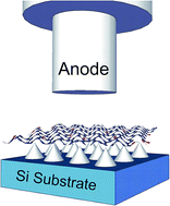
We report a simple and general solution-based methodology to support reduced graphene oxide layers (rGO) onto micro-spikes engraved on Si to produce high-aspect ratio wrinkles and sharp protrusions. It is observed that as the number of deposited rGO layers is increased the wrinkle density progressively increases complemented by a remarkable folding of graphene sheets at the vicinity of the spike tips. Highly efficient and stable field emission with low turn-on fields was observed, attributed to the local enhancement of the electric field at the wrinkled rGO protrusions. The ability to produce wrinkled graphene from solution could allow large area deposition providing prospects for the development of practical electron sources and advanced devices based on graphene oxide field emitters. The contribution of this hierarchical, hybrid film morphology is evaluated and discussed.


Introduction

Field electron emission (FE) or also known as cold cathode emission is a form of quantum mechanical tunnelling in which electrons pass through a barrier in the presence of an electric field. This phenomenon is highly dependent on both the material properties and the geometry of the cathode; under high vacuum conditions, a high aspect ratio emitter produces high field emission currents at low applied fields. Research in cathode field emitters known as vacuum microelectronics1 and recently as vacuum nanoelectronics2 is important for various applications, including electron guns,3 microwave power amplifiers,4 X-ray tubes,5 neutralizers for space propulsion devices,6 electron beam lithography7 and large-area field emission sources such as flat panel field emission displays (FEDs).8

A critical parameter for a FE cathode performance is the field enhancement factor β, which can be maximized by increasing the aspect ratio, β that is proportional to the emitter height over its tip radius. Owing to their unique geometries, 1D and 2D nanostructures, including nanotubes and nanosheets had attracted significant attention for FE applications. Indeed, due to their small tip curvatures, ranging from sub-nanometers to few nanometers, and relatively long lengths of few microns, the aspect ratio becomes increasingly high. As a result, such nanostructures could generate a large electric field enhancement capable of obtaining electron emission at pretty low applied fields. Currently, there is an increasing research interest to develop FE cathodes using 2D graphene sheets,9,10 owing to their outstanding optoelectronic, mechanical and chemical properties.

Among the most promising methods to further increase the performance of FE devices is based on the hierarchical development of the emitting cathode.11,12 According to this approach, the emitting surface comprises primary microstructures complemented with 1D or 2D nanoemitters. As a result the field enhancement process is performed in two steps, while the final β obtained is a function of the product of the enhancement factors corresponding to each step. Although the above approach gave rise to promising electron emission properties, there is a lot to be done in order to develop large area FE devices based on hierarchical cathodes.11

Here, we report on simple and general solution-based approach to produce large area graphene-based hierarchical FE cathodes. It should be noted here that typical deposition methods on planar substrates give rise to graphene sheets that tend to lie parallel to or protruding at small angles from the substrate, thus limiting the geometrical field enhancement. Our method is based on drop-casting of reduced graphene oxide (rGO) nanosheets on forests of conical micro-spikes engraved on Si (μSi:rGO). We show that, due to their anchoring onto the micro-spike apexes, the rGO nanosheets become extensively folded giving rise to high-aspect ratio wrinkles. The wrinkled, μSi:GO, cathodes were found to exhibit excellent FE performance and stability superior to that of thin-film-type rGO emitters prepared on flat substrates.

Experimental section

Preparation of the substrate

The micro-spike arrays were fabricated by femtosecond (fs) laser texturing of n-type Si wafers (resistivity of 2–8 Ω cm) in a reactive SF6 atmosphere, as described previously.13 Following laser irradiation, the samples were treated by a 10% HF aqueous solution in order to remove the oxide grown on the spikes' surface.

Fig. 1 shows the different aspect ratio micro-spike arrays, obtained after the laser structuring process at different irradiation fluences. Upon increase of the laser fluence the microspike's aspect ratio increases, while their areal density decreases. In all cases, the microspikes are well-separated and perpendicular to the substrate surface.


image file: c5ra23031d-f1.tif
Fig. 1 Picture of a laser structured Si wafer, showing the processed black microspike area (rightmost part). Representative SEM images of structured areas exhibiting low (LμSi), medium (MμSi) and high (HμSi) spike heights are additionally illustrated. The respective irradiation fluence, spike height, tip radius and aspect ratio are also shown.
Preparation of the rGO:μSi field emitters. Graphene oxide (GO) was prepared from purified natural graphite powder (Alfa Aesar, ∼200 mesh) according to a modified Hummer's method.14 Aqueous GO solution (0.5 mg mL−1) was obtained by sonicating specific quantity of GO powder in deionized (DI) water for 1.5 h using a bath sonicator (Elmasonic S30H). To prepare GO films, GO aqueous solution (3 mL) was placed into a beaker (10 mL) together with the microstructured Si substrates. Subsequently, the n-butanol was poured of on top of the GO solution, thereby forming an n-butanol/water interface. GO sheets started accumulating at the two-solvent interface, and a continuous GO layer was observed to be formed within 30 min. Subsequently, by gently removing most of the n-butanol, the GO layer was collected onto the Si spikes substrate. This layer coating procedure was repeated accordingly to form the 3-, 5-, 7- and 9-layered GO-coated Si spikes substrates respectively. In particular, for FSi:GO sample, GO films were collected over planar Si substrates, while for μSi:GO samples, HμSi:MμSi: and LμSi[thin space (1/6-em)]:[thin space (1/6-em)]GO, GO layers were collected on laser etched Si substrates comprising 3D arrays of high-, medium- and low-aspect ratio microspikes respectively.

Following the GO layers' deposition the coated substrates were exposed to N2H4 (98% Aldrich) vapors at 40 °C, for the reduction of the GO coating to rGO. In particular, the substrates were placed in a perfectly cleaned glass Petri dish and then inside a larger glass Petri dish, which contained N2H4 (10 μl). Subsequently, drops of N2H4 were placed in the space between the two dishes, around the small Petri dish. The larger dish was covered with a glass lid, sealed with Parafilm tape, and placed over a hot plate at 40 °C overnight. Thereafter, the dish was opened, the substrates were dried under a nitrogen stream and heated at 80 °C in vacuum. The first indication that the reduction process has taken place to the material is the change of the colour after the hydrazine vapor treatment, from yellowish-brown to metallic grey. Details can be found elsewhere.15 The surface morphology of the final coated structures was examined by field emission scanning electron microscopy (FESEM JEOL-JSM7000F), both before and after the FE measurements. Following the FE process, there was no apparent explosive destruction to the coating, which can be associated with discharge currents.

Preparation of the rGO:μSi field emitters

FE measurements were performed under high vacuum conditions (<10−6 torr), using the samples as cold cathode emitters in a short-circuit protected planar diode system. Details for the experimental setup can be found elsewhere.16 Current density–electric field (JE) curves were taken at the distance between anode–cathode was controlled by a stepper motor and found that field emission characteristics are not influenced by the anode height. All measurements presented here were performed at t = 200 μm. Several emission cycles were taken in order to verify the stability and the reproducibility of the JE curves. A voltage with variable sweep step, supplied by a high voltage (HV) source (PS350-SRS), was applied between the anode and the cathode to extract electrons. The turn on field, Eto, that is finally measured is the average macroscopic field needed to extract 25 pA cm−2. The emission current was measured using an auto-arranging digital Pico-ammeter (Keithley 485) protected against high voltage surges by a Metal Oxide Semiconductor-Field Effect Transistor (MOSFET) limiter. The stability of the emission current over time was examined by monitoring the evolution of the emitted current density over a long time period of continuous operation.

Results and discussion

Fig. 2 shows typical FESEM images of the rGO:μSi arrays. A general observation was that as the number of deposited GO layers is increased, the nanosheets progressively formed a wrinkled layer, covering the microspikes' area (Fig. 2e and f). In particular, for 1–3 layers (Fig. 2a and b) rGO nanosheets form a conformal layer covering the microspikes and the laser induced morphology was practically preserved, for 4–6 layers (Fig. 2c and d) microspikes were partially covered by an discontinuous wrinkled rGO layer and for 7–9 layers microspikes were completely covered by a continuous wrinkled layer (Fig. 2e and f).
image file: c5ra23031d-f2.tif
Fig. 2 Typical SEM images of rGO:μSi cathodes coated with 1–3 (a, b), 4–6 (c, d) and 7–9 (e, f) rGO layers. The arrows in (a–d) indicate the partial coverage of the microarrays by rGO sheets, while in (e–f) indicate the high-aspect ratio wrinkles created within the rGO layer as well as the substantial deformation of the rGO layer at the sites of the sharp spike tips.

Fig. 3a and b compares the FE characteristics of the rGO:μSi cathodes comprising 3 and 5 rGO layers respectively. Three distinct regions are always visible in the JE data presented in the insets: zero emission, field emission and current saturation. The current saturation observed at high fields can be attributed to either resistive heating or high contact resistance effects. A similar saturation effect had been observed in carbon nanotube (CNT)-based field emitters and is explained in terms of heating of the CNT tip as a rate-limiting step in the high field region.17 The high current densities reached in this region give rise to considerable heating of the rGO wrinkles and failure of the emission sites. Alternatively, a high rGO:μSi contact resistance may lead to inefficient electron supply at the maximum attainable current from the conduction band of Si that limits the emission current at high fields.18


image file: c5ra23031d-f3.tif
Fig. 3 FN plots of rGO:μSi cathodes with (a) 3 and (b) 5 rGO layers deposited onto μSi substrates with different spike aspect ratios shown in the legend and defined in the text. The insets present the respective logarithmic plots of current density–field (JE) emission characteristics.

For the study of the FE data we adopted the Fowler–Nordheim (FN) analysis of field-assisted tunnelling, which is widely used to describe the relationship between the current density J and the local field at the emitter Eloc, which is usually related to the average field E as follows:

 
image file: c5ra23031d-t1.tif(1)
where V is the voltage bias, d is the inter-electrode spacing and β is the geometric field enhancement factor. Within this frame the FN law is expressed as
 
image file: c5ra23031d-t2.tif(2)
where A = 1.54 × 10⁻⁶ A eV V−1 is constant which depends on the surface structure,19 bFN = 0.943/2 with B = 6.83 × 10⁷ V cm−1 eV−3/2, while Φ is the work function of the material in eV. Fig. 3a and b show the respective FN plots. The corresponding field enhancement factors can be determined by fitting the linear part of the data, following eqn (2), assuming a typical work function for rGO of 5.0 eV.20 It can be observed that the β value calculated for the medium and high aspect ratio rGO:μSi cathodes is higher than the best uncoated, HμSi array. Furthermore, as the microspike aspect ratio is increased, the emission threshold decreases. More importantly, for the same type of μSi:rGO cathode, the Eto decreases, while β remains constant or increases, as the number of deposited rGO layers is increased.

The observed enhancement of the FE performance may be attributed to the gradual formation of high aspect ratio wrinkles (Fig. 2c and e) within the graphene coating area, as the number of deposited rGO layers is increased. Besides this, high magnification SEM images (Fig. 2d and f, arrows) reveal that graphene layers become remarkably folded at the microspike tip sites. This effect is more pronounced in the case of rGO:HμSi cathodes, possibly due to the higher aspect ratio of the spikes and smaller tip radii. Our results comply with theoretical predictions, showing that electrons are easily emitted from the graphene wrinkles.21

Based on the above observations, we focused on the development of rGO:HμSi-based FE cathodes, fabricated by depositing an increasing number of rGO layers (1–9 layers) onto the highest aspect ratio, HμSi, substrates. Fig. 4 depicts representative FESEM images of the fabricated cathodes, which confirms the progressive formation of wrinkles and the remarkable deformation of graphene sheets at the vicinity of the spike tips (Fig. 4d, arrows). However, it is observed that after a certain number of deposited layers, the number density of wrinkles becomes lower, while the sheet deformation at the spike tips is less pronounced (Fig. 4e and f, arrows). In this case, the entire rGO film becomes too thick and thus it may be mechanically unfavorable to be folded to form wrinkles. The corresponding FE characteristics are presented in Fig. 5, while Table 1 summarizes the calculated FE parameters Eto and β. It is clear that the FE performance complies with the characteristics of wrinkles formation; therefore it is enhanced as the number of rGO increases from 1 to 7, when the wrinkle density progressively increases, until it is deteriorating again upon further deposition of rGO layers, when the wrinkling effect becomes less pronounced.


image file: c5ra23031d-f4.tif
Fig. 4 Typical cross-sectional SEM images of rGO:HμSi cathodes coated with 3 (a, b), 7 (c, d) and 9 (e, f) rGO layers. The arrows in (a–b) indicate the partial coverage of the microarrays by rGO sheets, while in (c–d) indicate the high-aspect ratio wrinkles created within the rGO layer as well as the substantial deformation of the rGO layer at the sites of the sharp spike tips.

image file: c5ra23031d-f5.tif
Fig. 5 (a) JE characteristics of the cathodes prepared by depositing different number of rGO layers onto HμSi arrays; (b) the respective FN plots of the FE characteristics shown in (a).
Table 1 Field emission properties of FE cathodes fabricated by depositing different number of rGO layers onto HμSi substrates, defined in the text. The ± values denote the standard deviation of each measured or estimated quantity
Number of layers 0 1 3 5 7 9
Eto (V μm−1) 5.8 ± 0.1 4.9 ± 0.1 3.7 ± 0.1 1.75 ± 0.1 1.3 ± 0.1 1.8 ± 0.1
β 58 ± 8 74 ± 11 161 ± 24 566 ± 65 βlow = 4819 ± 132 395 ± 51
βint = 1502 ± 86


Fig. 5 indicates that the best performance is attained for the cathode fabricated using 7 rGO layers. In this case Eto becomes as low as ∼1.3 V μm−1 which is comparable to the best rGO field emitters reported to date.13,22,23 Interestingly the lower part of the FN plot of this cathode displays a nonlinear relation between ln(J/E2) versus 1/E (Fig. 4b, blue symbols). This is different from the emission behavior exhibited by the rest of the cathodes tested. Indeed, the low and intermediate fields part of the FN plot can be sectioned into two regions of linear behavior. This behavior of the FN plot was observed to be reproducible for all the cathodes of the same type tested. The calculated β values from the slopes of the two linear sections are βlow = 4819 ± 132 and βint = 1502 ± 86 respectively. The observed nonlinearity may be attributed to the saturation of the conduction band current and predominance of valence band current at higher field values.24

It may also be explained by the increasing number of emission sites with increasing applied voltage.10 Further experiments are currently in progress to clarify the emission mechanism of wrinkled rGO supported on μSi arrays. It is also necessary to theoretically investigate the quantum tunneling mechanisms associated with the enhanced field emission from rGO sheets with nanometer scale wrinkle protrusions.

The stability of the FE current over time is crucial for device applications. Fig. 6 presents the evolution of the emission current density at constant field over a long period of continuous operation for the best emitting sample rGO:HμSi compared to the uncoated HμSi array. It can be observed tha the FE current emitted from rGO:HμSi cathodes remained stable over more than 35 hours of continuous operation. On the contrary, the emission current for the uncoated HμSi arrays dropped dramatically within a few hours.


image file: c5ra23031d-f6.tif
Fig. 6 Emission current stability over time at a constant field for the bare HμSi and the 7-layered rGO:HμSi cathode.

Conclusions

In conclusion, a simple and general solution-based methodology for the fabrication of wrinkled rGO cathode field emitters has been demonstrated. When an aqueous solution of rGO is deposited on Si micro-spikes, the rGO sheets are wrinkled and are substantially folded by the sharp spikes tips. It is shown that this methodology leads to rGO field emitters with low threshold field and remarkable stability. The ability to deposit wrinkled rGO sheets in large-scale will allow fundamental studies as well as shed light on technologically vial route to exploiting the unique 2D structure for applications.

Acknowledgements

This research has been co-financed by the European Union (European Social Fund–ESF) and Greek national funds through the Operational Program “Education and Lifelong Learning” of the National Strategic Reference Framework (NSRF)-Research Funding Program: ARCHIMEDES III. Investing in knowledge society through the European Social Fund.

Notes and references

  1. J. W. Han, J. S. Oh and M. Meyyappan, Appl. Phys. Lett., 2012, 100, 213505 CrossRef.
  2. T. Utsumi, IEEE Trans. Electron Devices, 1991, 38, 10 CrossRef.
  3. N. de Jong, Y. Lamy, K. Schoots and T. H. Oosterkamp, Nature, 2002, 420, 393 CrossRef PubMed.
  4. K. B. K. Teo, E. Minoux, L. Hudanski, F. Peauger, J.-P. Schnell, L. Gangloff, P. Legagneux, D. Dieumegard, G. A. J. Amaratunga and W. I. Milne, Nature, 2005, 437, 968 CrossRef CAS PubMed.
  5. G. Z. Yue, Q. Qiu, B. Gao, Y. Cheng, J. Zhang, H. Shimoda, S. Chang, J. P. Lu and O. Zhou, Appl. Phys. Lett., 2002, 81, 355–357 CrossRef CAS.
  6. L. F. Velasquez-Garcia, A. I. Akinwande and M. Martinez-Sanchez, J. Microelectromech. Syst., 2006, 15, 1272–1280 CrossRef.
  7. A. A. Fomani, A. I. Akinwande and L. F. Velasquez-Garcia, J. Phys.: Conf. Ser., 2013, 476, 012014 CrossRef.
  8. D. E. Engelsen, Proc. Phys. Soc., 2008, 1, 355–365 CrossRef.
  9. G. Viskadouros, D. Konios, E. Kymakis and E. Stratakis, Appl. Phys. Lett., 2014, 105(20), 203104 CrossRef.
  10. D. Ye, S. Moussa, J. D. Ferguson, A. A. Baski and M. S. El-Shall, Nano Lett., 2012, 12, 1265–1268 CrossRef CAS PubMed.
  11. E. Stratakis, RSC Nanosci. Nanotechnol., 2015, 35, 230–243 CAS.
  12. E. Stratakis, R. Giorgi, M. Barberoglou, T. Dikonimos, E. Salernitano, N. Lisi and E. Kymakis, Appl. Phys. Lett., 2010, 96, 043110–043112 CrossRef.
  13. V. Zorba, E. Stratakis, M. Barberoglou, E. Spanakis, P. Tzanetakis, S. H. Anastasiadis and C. Fotakis, Adv. Mater., 2008, 20, 4049 CrossRef CAS.
  14. W. S. Hummers and J. R. E. Offeman, J. Am. Chem. Soc., 1958, 80, 1339 CrossRef CAS.
  15. G. Viskadouros, M. M. Stylianakis, E. Kymakis and E. Stratakis, ACS Appl. Mater. Interfaces, 2013, 6(1), 388–393 Search PubMed.
  16. E. Stratakis, G. Eda, H. Yamaguchi, E. Kymakis, C. Fotakis and M. Chhowalla, Nanoscale, 2012, 4, 3069–3074 RSC.
  17. R. C. Smith, J. D. Carey, R. J. Murphy, W. J. Blau, J. N. Coleman and S. R. P. Silva, Appl. Phys. Lett., 2005, 87, 263105 CrossRef.
  18. M. Ding, H. Kim and A. I. Akinwande, Appl. Phys. Lett., 1999, 75, 823 CrossRef CAS.
  19. A. Modinos, Field, Thermionic, and Secondary Electron Emission Spectroscopy, Plenum, New York, 1984 Search PubMed.
  20. L. Sygellou, G. Viskadouros, C. Petridis, E. Kymakis, C. Galiotis and D. Tasis, RSC Adv., 2015, 5(66), 53604–53610 RSC.
  21. Y. Guo and W. Guo, J. Phys. Chem. C, 2013, 117, 692–696 CAS.
  22. Z. Luo, Y. Lu, L. A. Somers and A. T. C. Johnson, J. Am. Chem. Soc., 2009, 131, 898–899 CrossRef CAS PubMed.
  23. L. Jun, J. Chen, B. Luo, X. Yan and Q. Xue, AIP Adv., 2012, 2, 022101 CrossRef.
  24. A. A. Al-Tabbakh, M. A. More, D. S. Joag, I. S. Mulla and V. K. Pillai, ACS Nano, 2010, 40, 5585 CrossRef PubMed.

This journal is © The Royal Society of Chemistry 2016
Click here to see how this site uses Cookies. View our privacy policy here.