Mingxian Wang,
Weiguang Wang,
Zhao Li,
Xuejian Du,
Xianjin Feng,
Haisheng Xu,
Wei Zhao and
Jin Ma*
School of Physics Shandong University, Jinan 250100, PR China. E-mail: jinmasdu@163.com; Fax: +86 531 88564886; Tel: +86 531 88361057
First published on 6th January 2016
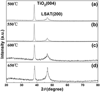
TiO2 thin films with anatase structure have been prepared on [LaAlO3]0.3[SrAl0.5Ta0.5O3]0.7 (LSAT) (001) substrates by metalorganic chemical vapor deposition (MOCVD) in the substrate temperature range of 500–650 °C. Tetrakis-dimethylamino titanium (TDMAT) is used as the organometallic source and oxygen as oxidant. Structural and optical properties of the films as well as the epitaxial mechanism have been investigated by X-ray diffraction (XRD), transmission electron microscopy (TEM) and optical transmittance spectra. The measurements and analyses show that the TiO2 film grown at 550 °C exhibits the best crystallinity with anatase structure. The obtained TiO2 film is a single-crystalline epitaxial film with no twins and very few defects. The heteroepitaxial relationship is determined as TiO2 (001) ‖ LSAT (001) with TiO2 [100] ‖ LSAT 〈100〉. The average transmittance of the film deposited at 550 °C in the visible wavelength is about 84% with an optical band gap of about 3.27 eV.
In the present work, high quality single crystalline anatase TiO2 thin films with no twins have successfully been prepared on LSAT (001) by MOCVD. The structural and optical properties of the films as well as the epitaxial relationships between the substrate and the anatase TiO2 film were investigated in detail. Preparation of high quality anatase TiO2 heteroepitaxial films will lay a good foundation for improving the doping efficiency of TiO2 materials and performance of TiO2-base semiconductor devices.
Ti(N(CH3)2)4 + 15O2 → TiO2 + 8CO2↑ + 2N2↑ + 12H2O↑ |
The out-of-plane epitaxial relationship of our samples was determined using a Rigaku D/MAX 2200PC X-ray diffractometer (XRD) with Cu Kα radiation. The Φ-scans were carried out with a X'Pert Pro MPD X-ray diffractometer with Cu Kα radiation to determine the in-plane epitaxial relationship. To further study the microstructure and epitaxial relationship of the samples, high-resolution transmission electron microscopy (HRTEM) and selected area electron diffraction (SAED) were performed with a Tecnai F30 transmission electron microscope operated at 300 kV on the cross-section of the sample prepared by gluing two pieces together with the thin films facing each other. The X-ray photoelectron spectroscopy (XPS) was employed to confirm the chemical composition of the prepared films using an ESCALAB MK II Multi-Technique Electron Spectrometer. The optical transmittance spectra were obtained using a TU-1901 double-beam UV-vis-NIR spectrophotometer in the wavelength range of 200–800 nm.
![]() | ||
Fig. 1 XRD spectra of the TiO2 samples deposited at different substrate temperatures of (a) 500 °C, (b) 550 °C, (c) 600 °C and (d) 650 °C. |
Fig. 2(a) and (b) shows the off-specular Φ-scans of the TiO2 {101} planes (ψ = 68.3°) for the film prepared at 550 °C and the {104} planes (ψ = 45.0°) for the LSAT (001) substrate at a fixed position. Fig. 2(a) shows four diffraction peaks separated by 90° from each other corresponding to the anatase TiO2 {101} planes, confirming the four-fold symmetry along c-axis of TiO2 with a tetragonal structure. Four sharp diffraction peaks with the same Φ-angles as those of the TiO2 {101} peaks are observed for substrate LSAT, indicating that the two lattices have the same coordinate system. These results reveal that the sample prepared in our study is single crystalline epitaxial with an in-plane orientation relationship of TiO2 [100] ‖ LSAT 〈100〉. The lattice mismatch between the film and substrate is about 2.3%.
![]() | ||
Fig. 2 Off-specular Φ-scans of (a) TiO2 {101} and (b) LSAT {101} planes at a fixed position for the sample deposited at 550 °C. |
XPS measurements was performed to confirmed the chemical elemental composition of our sample. The representative XPS survey spectrum for TiO2 film grown at 550 °C is displayed in Fig. 3(a). The peaks of Ti 2s, O 1s, Ti 2p and C 1s core levels as well as O KLL Auger peak can be observed, without any other elements observed, indicating the formation of titanium oxide.20 The C 1s peak is caused by the hydrocarbon contamination on the surface of the film. The peak positions have been calibrated using the C 1s peak at 284.6 eV as a reference due to the deviation originating from the charge accumulation at the surface of the film. Curves (b) and (c) show the Ti 2p and O 1s XPS spectra of the sample with deconvoluted and fit peaks, respectively. As can be seen in curve (b), the main sharp peak is located at the binding energy of around 458.4 eV, which is assignable to Ti 2p3/2 of Ti4+ as observed in TiO2 spectrum.21 In addition, a broad peak located at 464.2 eV with a peak-to-peak separation of 5.8 eV correspond to Ti 2p1/2 of Ti4+, which is also in accord with TiO2. No Ti3+ signals can be found at 457 eV, indicating the inexistence of Ti3+ on the surface of the thin film. Fig. 3(c) presents two fit peaks of O 1s and the spectrum consists of an intense main peak located at around 529.7 eV that is attributed to the Ti–O bonding in the TiO2 film, and the other weak peak at about 531.8 eV which can be regard as the C–O or OH− adsorbed species on the film surface.22 The stoichiometry of the films is determined by the relative areas of the fit peaks of O 1s (main peak at 529.7 eV) and Ti 2p with the correction of the elemental sensitivity factors. The atomic ratio of O and Ti is calculated and the value is about 2.0, which is accord with the stoichiometry of TiO2.
Further structural details of the sample grown at 550 °C were studied by TEM observations. Fig. 4(a) shows the cross-sectional low magnification TEM image of the film–substrate interface from which the thickness of the film is measured to be about 47.7 nm. The HRTEM and SAED micrographs of the interface area between TiO2 film and LSAT substrate are shown in Fig. 4(b). The incident electron beam is parallel to the [010] direction of the LSAT substrate. The SAED shows a typical single crystalline diffraction pattern and the diffraction spots of TiO2 (004), TiO2 (101), TiO2 (103), LSAT (001), LSAT (101) and LSAT (200) planes are clearly visible. In the HRTEM micrograph, a uniform and ordered lattice array in the interface region can be seen clearly without obvious transitional atomic layer, and an obvious interface of the film and substrate is marked by the white line. It is revealed that the deposited TiO2 film is an epitaxial film and the growth surface is TiO2 (001). For the TiO2 film portion, the lattice fringes corresponding to TiO2 (004) and (101) exhibits an angular separation of 68.0°, which is in good accordance with the standard calculated value of 68.3°. For the substrate, the lattice fringes corresponding to LSAT (001) and (101) with an angular separation of 45.6° can be seen. The SAED and HRTEM analyses of the interface for the sample show a clear epitaxial relationship of TiO2 (001) ‖ LSAT (001) which is consistent with the XRD results.
![]() | ||
Fig. 4 The cross-sectional (a) low magnification TEM, (b) HRTEM and SAED micrographs of the interface between TiO2 film grown at 550 °C and LSAT substrate. |
The good crystallinity and smooth morphology of the substrate contribute to the excellent epitaxial growth of TiO2 films. During the film deposition, TiO2 molecules are adsorbed by the LSAT substrate, and form nuclei on the substrate surface through the process of diffusion and condensation. The nuclei will constantly absorb molecules and steadily grow up into islands and expand into layer. Layer by layer repeatedly forms the well-crystalline epitaxial TiO2 films. The lattice constant of the LSAT substrate is large than that of the anatase TiO2, and the lattice mismatch along [100] direction is about 2.3%. Therefore, the anatase film epitaxially grown on the LSAT is under extension stress. In addition, the linear coefficient of thermal expansion of LSAT substrate and anatase TiO2 along [100] orientation are about 10 × 10−6 K−1 and 4.5 × 10⁻⁶ K−1, respectively. So the defects of the anatase crystal seen in the HRTEM micrograph can be attributed to the lattice mismatch and thermal expansion mismatch between the TiO2 film and the substrate. The critical thickness for the single crystal anatase film deposited on the LSAT substrate is about 8 nm estimated from the lattice mismatch. From the aspect of dynamic, the formation of misfit dislocation must overcome certain energy barrier, which makes the actual critical thickness considerably larger than the theoretical value, particularly when the substrates own a smooth surface. So the maximum possible thickness for our single crystal anatase TiO2 film is much larger than 8 nm, maybe reaches 100 nm.
The optical transmittance spectra of the TiO2 sample deposited at 550 °C and the bare LSAT substrate as a function of wavelength in the range of 200–800 nm are shown in Fig. 5. The average transmittance in the visible range of the sample is about 67%, and that of the LSAT substrate is about 79%. The absolute average transmittance for the film is about 84%. As a semiconductor with indirect band gap transition, the absorption coefficient (α) and optical band gap (Eg) have such a relationship: α(hv) = A(hv − Eg)2, where h is the Planck's constant, ν is the frequency of the incident photon and A is a material dependent constant. The inset shows the plot of (αhν)1/2 as a function of photon energy hv for the 550°C-deposited TiO2 sample. The Eg can be determined by extrapolating the straight-line portion of this plot to the energy axis, and the value is about 3.27 eV, which is similar to that of TiO2 samples annealed at 900 °C reported by D. J. Won et al.23
![]() | ||
Fig. 5 Optical transmittance spectra of the TiO2 sample deposited at 550 °C and the bare substrate, with the plot of (αhν)1/2 vs. hν for the sample deposited at 550 °C shown in the inset. |
This journal is © The Royal Society of Chemistry 2016 |