Xiaojiao Zhang‡
ab,
Min Zeng‡a,
Jiawei Zhangc,
Aimin Songc and
Shiwei Lin*ac
aKey Laboratory of Ministry of Education for Advanced Materials in Tropical Island Resources, College of Materials and Chemical Engineering, Hainan University, Haikou 570228, China. E-mail: linsw@hainu.edu.cn
bSchool of Applied Science and Technology, Hainan Tropical Ocean University, Sanya 572022, China
cSchool of Electrical and Electronic Engineering, University of Manchester, Sackville Street Building, Manchester M13 9PL, UK
First published on 14th January 2016
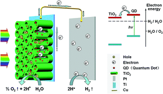
PbS and CdS quantum dots (QDs) were deposited on TiO2 nanotube arrays (TNTAs) by a sonication-assisted successive ionic layer adsorption and reaction (S-SILAR) method. Effects of the composite configuration, QD deposition order, and number of S-SILAR cycles on the photoelectrical properties have been systematically investigated. Depositing the TNTAs with PbS QDs before or after CdS QDs results in TNTAs/PbS/CdS or TNTAs/CdS/PbS configurations. The deposition order has been demonstrated to strongly affect the photoelectrochemical performance, and the TNTAs/PbS/CdS configuration shows the superior performance due to the synergistic effect of the different types of QDs. Studies of the photoelectrical properties of the TNTAs sensitized by single QDs with various number of S-SILAR cycles suggest that PbS decoration can dramatically increase the photocurrent density, and CdS can stabilize the photoelectrochemical behavior. Combining both beneficial effects of these two kinds of QDs, the TNTAs sensitized by 5 cycles PbS and 5 cycles CdS (referred to as TNTAs/PbS(5)/CdS(5)) can achieve the photocurrent density of 0.87 mA cm−2 under a white light source irradiation of 5.9 mW cm−2, corresponding to a record normalized photocurrent of 147 mA W−1. And the photoconversion efficiency can reach 14.3%. Further time-dependent measurement shows that TNTAs/PbS(5)/CdS(5) possesses a stable photoresponse for more than 120 min.
So far, many studies have been reported to cosensitize TiO2 with various semiconductor materials such as CdSe/CdTe,6 CdS/CdSe,7 CdS/CdSe/ZnS,8 PbS/CdS,9 and so on. Among them, PbS/CdS is one of the most promising narrow-band-gap semiconductor combinations, since PbS with narrow band gap can harvest the infrared photons,5 and CdS has the proper conduction and valence band edges straddling the water oxidation and hydrogen reduction potentials.10 Many approaches have been developed to deposit QDs onto TiO2, such as close space sublimation,11 chemical bath deposition,12 self-assembly monolayer,13 cyclic voltammetric electrodeposition,14 and sonication-assisted chemical bath deposition.15 In this work, PbS and CdS QDs were deposited onto TiO2 nanotube arrays by a sonication-assisted successive ionic layer adsorption reaction (S-SILAR) method, which combined the advantage of both sonication and SILAR methods. The precursor solution was thus easy to penetrate into the nanotubes, leading to uniform and effective QD deposition on the TNTAs.
Herein several QD sensitizing configurations have been examined, including the deposition of PbS, CdS, PbS/CdS, and PbS/CdS QDs on the TNTAs. The investigation of the influence of QD deposition order and cycles suggests that TiO2 nanotube arrays sensitized by 5 cycles of PbS and then 5 cycles of CdS (referred to as TNTAs/PbS(5)/CdS(5)) possess the superior photoelectrochemical performance under visible-light excitation. A maximum photocurrent density can rise to about 0.87 mA cm−2 under a white light source irradiation (553 ± 119 nm, 5.9 mW cm−2), and the photoconversion efficiency reaches a promising 14.3%. Systematic examination of the underlying mechanism suggests the synergistic effects from both types of QDs.
![]() | ||
Fig. 1 Diffuse reflectance absorption spectra of TNTAs/CdS(5), TNTAs/PbS(2), TNTAs/CdS(5)/PbS(2) and TNTAs/PbS(2)/CdS(5). |
The current density of the photoanodes has been measured in both dark and illumination conditions. As shown in Fig. 2, the saturated photocurrent densities are 0.14 ± 0.01, 0.23 ± 0.01, 0.25 ± 0.01 and 0.36 ± 0.01 mA cm−2 for TNTAs/CdS(5), TNTAs/PbS(2), TNTAs/CdS(5)/PbS(2) and TNTAs/PbS(2)/CdS(5), respectively. The TNTAs co-sensitized with both types of QDs shows better photocurrent densities than those of the photoanodes sensitized with single QDs. And the TNTAs/PbS(2)/CdS(5) exhibits much higher photocurrent density than the others. Although the visible-light absorption intensity is a little weaker than that of TNTAs/CdS(5)/PbS(2) (Fig. 1), TNTAs/PbS(2)/CdS(5) shows much better photocurrent density, which suggests the significance of the QD deposition order to improve the photoresponse. A close inspection of the J–V curves shows that TNTAs/PbS(2) and TNTAs/CdS(5)/PbS(2) present apparent dark currents, which might be related to the PbS self-corrosion and/or the electrons in the conduction band recombination with the electrolyte.20 But the dark current becomes negligible when CdS QDs were deposited at the outer layer, which indicates the PbS self-corrosion and/or electron recombination could be effectively prevented. This is in a good agreement with the previous finding where the presence of the CdS and ZnS passivation layers coating on the PbS QDs could greatly suppresses the recombination of electrons residing on PbS with acceptor species in the electrolyte.21 To further clarify the underlying mechanism for the enhancement of QD cosensitization, surface morphology and detailed microstructure will be necessary to investigate.
![]() | ||
Fig. 2 J–V curves in dark (dash lines) and illumination (solid lines) conditions for TNTAs/CdS(5), TNTAs/PbS(2), TNTAs/CdS(5)/PbS(2) and TNTAs/PbS(2)/CdS(5). |
Fig. 3 displays the SEM and EDS results of TNTAs/CdS(5)/PbS(2) and TNTAs/PbS(2)/CdS(5), which show the effectiveness of the sonication-assisted approach for depositing CdS and PbS QDs on the TNTAs. Different configurations are found to result in different surface morphology. Fig. 3a shows that QDs aggregate at the entrance of TNTAs/CdS(5)/PbS(2), while Fig. 3b presents a high dispersibility and uniform deposition of QDs on TNTAs/PbS(2)/CdS(5). EDS results in Fig. 3c and d indicate that the atomic ratio of the sum of Cd and Pb to S in different samples tested is close to 1:
1 which confirms the stoichiometric formation of CdS and PbS. However, the QD loading amounts of TNTAs/CdS(5)/PbS(2) appear different from those of TNTAs/PbS(2)/CdS(5) due to the different surface conditions of loading. For example, the atomic ratio of Pb in TNTAs/CdS(5)/PbS(2) is bigger than that in TNTAs/PbS(2)/CdS(5), which might be attributed to more absorption sizes for Pb2+ deposition on TNTAs/CdS(5) than on TNTAs. As a result, in Fig. 1, the absorption onset of TNTAs/CdS(5)/PbS(2) is longer than that of TNTAs/PbS(2)/CdS(5).
Furthermore, XRD patterns were recorded to characterize the crystal structure of the photoanodes (ESI, Fig. S1†). Two diffraction peaks at 25.3° and 48.1° can be clearly observed, which correspond to TiO2 anatase (101) and (200) planes (JCPDS 21-1272). However, no signature can be detected for PbS and CdS crystals probably due to their quite low deposition amount. The detailed crystal structure of the QDs deposited on the TNTAs can be confirmed by the TEM images in Fig. 4. As shown from the high-resolution TEM (HRTEM) images in Fig. 4a and b, the calculated lattice fringe spacings of 0.295 nm and 0.336 nm correspond to the (200) plane of PbS cubic phase (JCPDS 05-0592) and the (111) plane of CdS cubic phases (JCPDS 89-0440), respectively. The lattice spacing of 0.352 nm is assigned to the (101) plane of anatase phase TiO2 (JCPDS no. 21-1272), which is in good agreement with the XRD pattern. Compared with the TEM image of the untreated TNTAs (Fig. S2†), the HRTEM images show PbS and CdS QDs evenly deposited on the inside and outside of the TNTAs and confirm their sizes of nanoparticles. The QD size and distribution can be influenced by precursor concentration.22 For a low precursor concentration (PbS 0.02 M), uniform and small particles were formed in the TNTAs/PbS(2) (see the inset of Fig. 4a), while for relatively high precursor concentration (CdS 0.05 M), some irregular large particles or aggregations were formed in the TNTAs/CdS(5) (see the inset of Fig. 4b). A comparison of the TEM images of TNTAs/CdS(5)/PbS(2) and TNTAs/PbS(2)/CdS(5) demonstrates the well-separated and uniformly QDs deposition on the TNTAs/PbS(2)/CdS(5). This might be attributed to the small and uniform PbS QDs as the seed to control the size and distribution of the final QDs. It has been demonstrated that the CdS QD light-absorbing layer could act as a passivation layer to reduce the recombination.23,24 Thus the CdS overcoating onto the TNTAs/PbS is expected to improve the photoelectrochemical performance.
![]() | ||
Fig. 4 TEM images of (a) TNTAs/PbS(2), (b) TNTAs/CdS(5), (c) TNTAs/CdS(5)/PbS(2) and (d) TNTAs/PbS(2)/CdS(5). The insets show the corresponding TEM images with a relatively low magnification. |
In order to study the effect of deposition cycles on the photoelectrical properties, single QDs with various S-SILAR cycles have been deposited onto the TNTAs, and their photoresponse was examined (Fig. 5). As the deposition cycle increases, the photocurrent density increases up to the optimal cycles and then decreases with further increasing the S-SILAR cycles. The TNTAs sensitized with CdS QDs exhibit a superior photocurrent density (0.38 ± 0.01 mA cm−2 at 0.4 V vs. SCE) when 14 S-SILAR cycles was applied (Fig. 5a). As for the TNTAs sensitized with PbS QDs, a much better photocurrent density 0.73 ± 0.01 mA cm−2 can be achieved at 0.4 V vs. SCE with 5 S-SILAR cycles. The enhancement of photocurrent density can be ascribed to the increased light harvesting and effective charge separation with increasing QD deposition. However, the photocurrent density begins to decline as the deposition cycles rise beyond the optimal cycles, which can be attributed to the QDs aggregation and the mismatch of the conduction and valence band edges due to the size-dependent alignment of energy levels in TiO2/QDs heterostructures.25,26 As the QD size increases with the increasing deposition cycles, the energy band edge alignment of TiO2/QDs heterostructure might change from type II to type I, in which case a photoinduced electron transfer across the interface is energetically blocked.27
![]() | ||
Fig. 5 J–V curves of the TNTAs sensitized by single QDs with different deposition cycles in dark (dash lines) and illumination (solid lines) conditions: (a) TNTAs/CdS, (b) TNTAs/PbS. |
Fig. 6 shows the surface morphology and EDS spectra of TNTAs/CdS(14) and TNTAs/PbS(5). The TNTAs is densely covered by large CdS nanoparticles in TNTAs/CdS(14) (Fig. 6a), while relatively small PbS QDs uniformly distribute on the nanotube arrays in TNTAs/PbS(5) (Fig. 6b). The values of Cd:
S and Pb
:
S atomic ratios are around 1
:
1, confirming the stoichiometric formation of CdS and PbS QDs. In terms of the QD loading amount on the TNTAs related to the best photocurrent density, the sum of the weight percentages of Cd and S elements is about 30 wt% in TNTAs/CdS(14), while only 6 wt% of Pb and S elements could achieve the maximum photocurrent density in TNTAs/PbS(5). This indicates that the photoelectrochemical performance of QDs deposited TNTAs depends not only on the QD deposition cycles (Fig. 5), but also on their deposition order (Fig. 2). Based on the results above, therefore, we can find out the optimum photoelectrical properties using the composite configuration with proper QD deposition order and cycles.
The combination of CdS and PbS QDs was then conducted by fixing the optimum cycles of one type of QDs and varying the cycles of the other type of QDs. And their optical and photoelectrical properties have been systematically examined. For clarity, only the representative results have been highlighted below. The light absorption properties of different configurations are presented in Fig. 7a, including TNTAs/PbS(5), TNTAs/CdS(14), TNTAs/PbS(5)/CdS(5) and TNTAs/PbS(5)/CdS(14). Decoration of PbS QDs on the TNTAs broadens the visible-light response until around 800 nm, corresponding to the PbS QDs' band gap of 1.55 eV by the empirical equation Eg = 1240/λ.28 Covering CdS QDs over the PbS QDs on the TNTAs does not apparently change the absorption intensity in the visible region. It is expected that the photoelectrical properties of the TNTAS co-sensitized with QDs are strongly dependent on the energy-level alignment at the interfaces.
The relative energy levels of bulk TiO2, PbS and CdS are shown in Fig. 7b.29–31 Although the conduction band position of PbS bulk is much lower than that of TiO2, the up shift of the conduction band as well as the valence band can be achieved from the quantum confinement effect by modifying the average size of the PbS domain in a quantum-size scale.17 The redistribution of the electrons leads to a stepwise band structure due to Fermi level alignment (Fig. 7c). The resulting structure is favorable for electron injection from the conduction band of CdS into that of PbS and eventually arriving at the conduction band of TiO2, which may contribute to a remarkable enhancement of the photoelectrochemical performance.
The J–V results in Fig. 5b have suggested that TNTAs/PbS(5) has a suitable staggered alignment of conduction and valence band edges at the TNTAs/PbS interface. On the other hand, CdS has already possessed favorable band positions in its bulk state for electron injection into the conduction band of TiO2.29 However, in order to build a optimal stepwise band-edge structure in the TNTAs/PbS(5)/CdS photoanode, one should modify the CdS QD size and maximize the photocurrent response.
Overcoating 5 S-SILAR cycles of CdS QDs on the TNTAs/PbS(5) presents the superior photoelectrochemical performance as shown in Fig. 8. At −0.4 V vs. SCE, the photocurrent densities of TNTAs/PbS(5)/CdS(5), TNTAs/PbS(5)/CdS(14), TNTAs/PbS(5), TNTAs/CdS(14), are 0.87 ± 0.02 mA cm−2, 0.85 ± 0.01 mA cm−2, 0.78 ± 0.01 mA cm−2, 0.36 ± 0.01 mA cm−2, respectively (Fig. 8a). Considering the intensity of the white-light excitation source is 5.9 mW cm−2, the normalized photocurrent of TNTAs/PbS(5)/CdS(5) can be calculated as 147 ± 3 mA W−1, which can directly illustrate the relationship between the generated photocurrent density and the applied illumination intensity. This result is more than those of the other similar QDs modified TNTAs reported up to now.16 To quantitatively analyze the efficiency of the photoelectrodes for PEC water splitting, the photoconversion efficiency can be calculated from the J–V curves.14 As shown in Fig. 8b, the photoconversion efficiencies are 14.3%, 8.6%, 12.5% and 3.6% for the TNTAs/PbS(5)/CdS(5), TNTAs/PbS(5)/CdS(14), TNTAs/PbS(5), and TNTAs/CdS(14), respectively. The photoconversion efficiency of TNTAs/CdS(14) is in agreement with that of the CdS-modified TiO2 nanocrystalline photoanode.30 The TNTAs/PbS(5)/CdS(5) photoanode has the maximum photoconversion efficiency of 14.3%, which exhibits about 4 times enhancement over the efficiency of the TNTAs/CdS(14). Among all the samples investigated, the TNTAs/PbS(5)/CdS(5) possesses the highest photocurrent density and superior photoconversion efficiency, which benefits from the uniform deposition of hybrid QDs and effective charge transfer between the hybrid QDs and TNTAs.
![]() | ||
Fig. 8 (a) J–V curves and (b) the corresponding photoconversion efficiencies of TNTAs/PbS(5), TNTAs/CdS(14), TNTAs/PbS(5)/CdS(5) and TNTAs/PbS(5)/CdS(14). |
We also use electrochemical impedance spectroscopy to further study the charge transfer characteristics of the photoelectrodes. Bode phase plots and Nyquist plots for various QDs sensitized TNTAs are shown in Fig. 9a and b, respectively. Typically, three characteristic frequency peaks can be observed in the Bode phase plots of the impedance spectra.31 The low-frequency peak (in the mHz range) corresponds to the Nernstian diffusion within the electrolyte, the middle-frequency peak (in the 1–100 Hz range) reflects the electron transfer in the photoanode and charge reaction at the photoanode/electrolyte interface, and the high-frequency peak (in the kHz range) corresponds to the charge-transfer at the counter electrode.31,32 In Fig. 9a, the low-frequency peak cannot be clearly distinguished since it vanishes underneath the middle-frequency peak due to the low resistance of the electrolyte. And the peaks at around 1 kHz can be attributed to the high-frequency peaks whose positions are fixed for the four different QDs sensitized TNTAs. The positions of the middle-frequency peaks are found to be strongly dependent on the QDs deposited on the TNTAs. Although it is hard to accurately determine the exact position of the middle-frequency peak which overlaps with the high-frequency peak, one can still clearly observe the peaks moving from high frequency to low frequency for TNTAs/PbS(5), TNTAs/PbS(5)/CdS(5), TNTAs/PbS(5)/CdS(14), and TNTAs/CdS(14) in sequence.
![]() | ||
Fig. 9 Electrochemical impedance spectra: (a) Bode phase plots and (b) Nyquist plots of TNTAs/PbS(5), TNTAs/CdS(14), TNTAs/PbS(5)/CdS(5) and TNTAs/PbS(5)/CdS(14). |
The location of the middle-frequency peak is closely linked with the effective electron lifetime, which can be estimated by τeff ≈ 1/2πf.31,33 Thus, among the photoanodes measured, TNTAs/PbS(5) has the shortest electron lifetime, indicating the remarkable recombination via surface states caused by PbS deposition. And the electron lifetime increases with increasing S-SILAR cycles of CdS QDs deposited on the TNTAs/PbS(5). This suggests that CdS deposition might passivate the surface traps and efficiently suppress electron recombination to improve the PEC performance of the heterojunction structure.
The charge transfer resistance at the photoanode/electrolyte interface can be evaluated from the arc diameters in the Nyquist plots (Fig. 9b),34,35 and quantitatively determined using the Randles–Ershler model within the intermediate frequency (0.1–100 Hz).36 Upon fitting with the equivalent circuit model (Fig. S3†), the values of the charge transfer resistance Rct could be obtained as shown in Table S1.† TNTAs/PbS(5) has the smallest charge transfer resistance, suggesting a favorable environment for charge transfer across the interface. Overcoating CdS on TNTAs/PbS(5) would increase the charge transfer resistance. However, TNTAs/PbS(5) does not possess as superior PEC performance as TNTAs/PbS(5)/CdS(5) (Fig. 8) due to the large electron recombination and dark current in TNTAs/PbS(5). Deposition of CdS QDs onto the TNTAs/PbS(5) can repress the recombination and protect PbS from self-corrosion. With the favorable staggered alignment of conduction band edges for electron transfer across the interfaces, TNTAs/PbS(5)/CdS(5) shows the optimum photoelectrical properties. However, as the CdS S-SILAR cycles keep increasing, the photocurrent density decreases due to the increase of the charge transfer resistance.
Furthermore, Fig. 10 shows the time-dependent photocurrent densities of the TNTAs/PbS(5), TNTAs/PbS(5)/CdS(5) and TNTAs/PbS(5)/CdS(14) measured at 0 V versus SCE under a white light irradiation of 5.9 mW cm−2. The results demonstrate that all the three photoelectrodes have a fast photoresponse when the light is turned on or off. The photocurrent density quickly decays at the beginning about five minutes. The reason is not clear at the moment but it might be related to the accumulation of charge carriers near the photoelectrode/electrolyte interface and/or the relatively slow oxidation kinetics.37,38 TNTAs/PbS(5) exhibits a relatively poor photostability as the photocurrent density steadily declines. Deposition of CdS on the TNTAs/PbS(5) can effectively improve the photochemical stability, where TNTAs/PbS(5)/CdS(5) shows a stable photocurrent for more than 120 min. In terms of longer photochemical stability, future work is required to modify the surface by either overcoating protective oxide layer, or integrating electrochemical cocatalysts.
![]() | ||
Fig. 10 Time-dependent photocurrent densities of TNTAs/PbS(5), TNTAs/CdS(5)/PbS(5) and TNTAs/PbS(5)/CdS(14). |
Footnotes |
† Electronic supplementary information (ESI) available. See DOI: 10.1039/c5ra22964b |
‡ Contributed equally to this work. |
This journal is © The Royal Society of Chemistry 2016 |