Effect of RF power on the structural, optical and gas sensing properties of RF-sputtered Al doped ZnO thin films

N. Srinathaa, Y. S. Nob, Vinayak B. Kamblec, Sujoy Chakravartyd, N. Suriyamurthye, Basavaraj Angadi*a, A. M. Umarjif and W. K. Choib
aDepartment of Physics, Bangalore University, Bangalore 560 056, India. E-mail: brangadi@gmail.com
bInterface Control Research Center, Future Convergence Research Division, Korea Institute of Science and Technology, SungbukGu, Hwangro 14 gil 5, Seoul 136-701, Republic of Korea
cSchool of Physics, Indian Institute of Science Education and Research, Thiruvananthapuram 695016, India
dUGC-DAE Consortium for Scientific Research, Kalpakkam Node, Kokilamedu-603104, India
eRadiological Safety Division, Indira Gandhi Centre for Atomic Research, Kalpakkam 603102, India
fMaterials Research Centre, Indian Institute of Science, Bangalore-560 067, India

Received 30th October 2015 , Accepted 14th January 2016

First published on 18th January 2016


Abstract

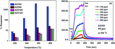
The effect of Radio Frequency (RF) power on the properties of magnetron sputtered Al doped ZnO thin films and the related sensor properties are investigated. A series of 2 wt% Al doped ZnO; Zn0.98Al0.02O (AZO) thin films prepared with magnetron sputtering at different RF powers, are examined. The structural results reveal a good adhesive nature of thin films with quartz substrates as well as increasing thickness of the films with increasing RF power. Besides, the increasing RF power is found to improve the crystallinity and grain growth as confirmed by X-ray diffraction. On the other hand, the optical transmittance is significantly influenced by the RF power, where the transparency values achieved are higher than 82% for all the AZO thin films and the estimated optical band gap energy is found to decrease with RF power due to an increase in the crystallite size as well as the film thickness. In addition, the defect induced luminescence at low temperature (77 K) and room temperature (300 K) was studied through photoluminescence spectroscopy, it is found that the defect density of electronic states of the Al3+ ion increases with an increase of RF power due to the increase in the thickness of the film and the crystallite size. The gas sensing behavior of AZO films was studied for NO2 at 350 °C. The AZO film shows a good response towards NO2 gas and also a good relationship between the response and the NO2 concentration, which is modeled using an empirical formula. The sensing mechanism of NO2 is discussed.


1. Introduction

In recent years, there has been an ever increasing technological demand for electronic devices with improved properties. ZnO is one of the most promising materials for many applications due to its wide band gap (3.27 eV) and large exciton binding energy of 60 meV, which is twice as large as that of GaN (28 meV).1 By virtue of its extraordinary properties, ZnO finds its applications in the fields of opto-electronics,2 spintronics,3,4 electro-luminescence displays5 and gas sensors.6 Recently, Al doped ZnO films have shown great promise as an alternative to the costlier Indium Tin Oxide (ITO), due to their low cost, non-toxicity and abundant availability compared to ITO films. The Al doped ZnO (AZO) films not only exhibit good electrical conductivity along with high optical transparency in the visible wavelength region (400–800 nm) but also offer good chemical, mechanical and thermal stability.

Besides, ZnO is one of the most extensively studied metal oxide semiconductor materials, next to SnO2 for the toxic and hazardous gas sensors.7,8 It is well known that the sensitivity of metal oxide semiconductor gas sensors can be improved upon doping or the addition of catalyst. Hence, it would be interesting to study the sensing properties of Al doped ZnO. Further, tuning the film thickness and the surface morphology plays a major role in order to enhance the sensitivity. Usually, controlling the film thickness and the morphology results in the increase of effective surface area, leading to improved gas adsorption. Moreover, the use of additives acts as catalysis for the solid–gas reaction for enhancing the sensitivity. The surface morphology is modified either by thermal treatment or by varying the processing parameters.

Till date, there are numerous reports on the undoped and doped metal oxide semiconducting sensors to sense different gases.9–12 There are many reports on NO2 gas sensors such as, SnO2,13 NiO,14 ZnO15–17 based sensors. Among all the existing metal oxide gas sensors, ZnO based sensors are attracting wide attention when it is doped with Al due to the high sensitivity towards NO2 and selectivity among other gases.9,15,18,23 Also there are many fabrication techniques have been introduced in literature to synthesize Al doped ZnO sensors.15,16,19,20,21,23,24 Among all, r.f magnetron sputtering technique15,19,24 has its own advantages to produce good quality of films having high surface area and surface roughness which are pre-requisite for the gas sensing. In addition, many parameters can be varied in order to obtain good quality of films with high reproducibility.

Hence, in the present investigation, we have studied the effect of RF power on the Zn0.98Al0.02O thin films properties such as, structural and morphological parameters. The optical band gap and luminescence properties have been studied to probe the electronic structure of the material. Finally, the gas sensing properties of AZO films deposited at different RF powers have been studied and the possible sensing mechanism is discussed.

2. Experimental

The Zn0.98Al0.02O (AZO) films were deposited on clean quartz substrates for 10 min at room temperature (RT) with varied RF power from 50 to 120 W under pure Ar plasma. The experimental details are found elsewhere.24 The AZO thin films deposited at the different RF powers 50, 80, 100 and 120 W are labelled as AZO50, AZO80, AZO100 and AZO120 respectively. The following systematic studies were carried out to understand the effect of RF power on the AZO film properties and gas sensing behaviour.

2.1 Characterization of the AZO thin films

The AZO thin films were characterized through GIXRD Bruker D8 Discover, 45 kV, 100 mA using Cu Kα radiation of wavelength 1.5418 Å. The effect of deposition conditions and RF power on the crystallinity and phase were studied. The microstructure and thickness of the films were studied through FEI Insitron Field Emission Scanning Electron Microscope (FESEM). The surface topographic features were examined though Atomic Force Microscope (AFM) images recorded on an APE Research AFM A100 instrument in contact mode. Further, the thin films were studied through Raman spectroscopy using the laser excitation source of wavelength 530 nm and power 15 mW on Horiba Jobin Vyon HR Raman – micro PL spectrometer. The optical band gap was calculated through UV-visible (ultraviolet–visible–near infrared) spectrophotometer, Ocean Optics, USB4000-XR, USA. The photoluminescence measurements were carried out at room temperature and at 77 K with a Jyobin Yvon Spectroflourometer Fluorolog-3 equipped with 450 W xenon lamp as excitation source.

2.2 Measurement of the gas sensing properties

The sensor response of the AZO films deposited at different RF powers for NO2 gas was studied by exposing AZO films to the respective test gas diluted with zero air. The details of the gas sensor characterization setup can be found elsewhere.25 The % response (S) was calculated using eqn (1);
 
image file: c5ra22795j-t1.tif(1)
where, Rg and Ra are the sensor resistances in presence of test gas and air, respectively.

The sensors were tested on exposure of 100 to 600 ppm concentration of NO2 gas at 350 °C.

3. Results and discussion

3.1 X-ray diffraction (XRD)

The GIXRD patterns of AZO films with different RF power are depicted in Fig. 1. It is seen that, all the peaks could be indexed to the JCPDS card no. 36-1451 corresponding to the hexagonal wurtzite ZnO phase with space group P63mc. A clear observation from XRD pattern shows that, the films are polycrystalline in nature, with a preferred orientation along c-axis i.e. (002) plane and a certain fraction along (103) plane. Further it is observed that, with increase of RF power, the (002) peak intensity decreases and concurrently the (103) peak intensity increases (top inset of Fig. 1), from which it is evidenced that the crystals are trying to change their orientation from (002) plane towards (103) plane when RF power is increased. In addition, the peaks shift has been observed with RF power (inset of Fig. 1). The parameters of Full Width at Half Maximum (FWHM) values of (002) peaks were calculated and tabulated in Table 1, which shows a decreasing trend with RF power, while the intensity of the (002) reflection increases with increase in the RF power, which indicates the increase of crystalline nature of the films. The crystallite size was calculated for highest intensity peak, i.e. (002) peak using Scherrer's formula shown in eqn (2)
 
image file: c5ra22795j-t2.tif(2)
where, k is the Scherrer's constant, λ is the X-ray wavelength, β is the observed FWHM, and θ is the Bragg's angle. It is found that, the estimated crystallite size increases with increase in RF power (Table 1). Furthermore, the lattice parameter ‘c’ is estimated using the equation c = λ/sin[thin space (1/6-em)]θ, where λ is the X-ray wavelength and θ is the Bragg diffraction angle corresponds to (002) peak. Also, the inter-planar spacing (d) was determined using Bragg's law equation; = 2d[thin space (1/6-em)]sin[thin space (1/6-em)]θ.

image file: c5ra22795j-f1.tif
Fig. 1 GIXRD pattern of Zn0.98Al0.02O for various RF power.
Table 1 Estimated lattice parameter, inter-planar distance, dislocation density, crystallite size and strain from XRD data
AZO films with different RF power/(Watts) FWHM of (002) peak x (π/180) radians d/(Å) FWHM of (103) peak x (π/180) radians d/(Å) Crystallite size, Dsch/(nm) a/(Å) c/(Å) δ/(1014 lines m−2) ε/(10−4)
(002) peak (103) peak Avg size
50 0.4147 2.5945 0.8222 1.4743 20.1 11.3 15.7 3.254 5.190 40.57 30.56
80 0.4014 2.5938 0.8003 1.4741 20.8 11.6 16.2 3.255 5.188 38.10 29.75
120 0.3652 2.5953 0.7778 1.4740 22.8 12.0 17.4 3.250 5.191 33.03 28.91


For a hexagonal crystal system, the lattice parameters were determined by using the following eqn (3);

 
image file: c5ra22795j-t3.tif(3)

The estimated lattice parameters (a = b & c) and inter-planar spacing (d) values are found to be in agreement with standard values of JCPDS card no. 36-1451 and are tabulated in Table 1.

The dislocation density (δ), defined as the length of dislocation lines per unit volume, is estimated using the relation (4);

 
image file: c5ra22795j-t4.tif(4)

The strain (ε) present in the thin films is estimated using the relation (5);

 
image file: c5ra22795j-t5.tif(5)

The estimated dislocation density (δ) and the strain (ε) are also summarized in Table 1. Hence it is inferred that, the δ and ε values decrease with increase of RF power due to decrease in the concentration of lattice imperfections.

3.2 Atomic force microscopy (AFM)

The Atomic Force Microscopy (AFM) micrographs of AZO50 and AZO120 thin films are depicted in Fig. 2. From the figure, the appearance and the density of the spike like features on the surface indicate the uniformity and nanocrystalline nature of the films. The film thickness is observed to be increasing with increase of RF power. The surface topographic parameters such as average roughness (Ra), rms roughness (Rrms) and the skewness (RSk) and kurtosis (RKu) parameter are measured and are summarized in Table 2. It is observed that, the average roughness of the film surface decreases with RF power indicating the uniform surface i.e. the increase of RF power makes thicker films with higher degree of uniformity of the films. The parameters such as skewness (RSk) and kurtosis (RKu) are a measure of the asymmetry and the sharpness, respectively. In particular, the skewness (RSk) is used to measure the profile symmetry about mean line. Hence, skewness (RSk) can either be zero, positive or negative. If the height distribution is symmetrical, the skewness factor RSk is zero. If the height distribution is asymmetrical, and the surface has more peaks than valleys, the skewness (RSk) is positive and if the surface is more planar and valleys are predominant the skewness (RSk) is negative. In present study of the AZO films, the skewness parameter, RSk is found to be positive, which reflects an asymmetrical height distribution and the surface of the films has more peaks than the valleys. Further, with increase of RF power, the RSk is found to decrease and the values are approaching zero, which indicates the decrease of surface peaks. Furthermore, AFM surface topographic parameter such as kurtosis (RKu) is a measure of surface sharpness of the films surface. If RKu is 3, indicates a Gaussian amplitude distribution, and the surface is called mesokurtic, but if kurtosis is smaller than 3 the surface is flat and called ‘Platykurtic’. If the kurtosis is higher than 3, the surface has more peaks than valleys. For AZO50 films, the RKu is found to be higher than 3, indicating the surface has more peaks than valleys, which further decreases with increase of RF power. Both the AFM as well as SEM results together shows the increase of surface smoothness and the thickness of the AZO films with increase of RF power. For specific applications such as sensors, the surface of the film plays a crucial role, which has been discussed in later part of this paper. If the surface of the film having high surface area with more peaks than valleys are the ideal for the sensing applications. In particular, in this case, the AZO50 film shows high surface area than other films prepared with higher RF power. Furthermore, the results of the sensing properties of AZO films are discussed in following sections.
image file: c5ra22795j-f2.tif
Fig. 2 AFM micrographs of AZO films.
Table 2 Summary of AFM analysis
Films Ra/(nm) Rms/(nm) Skewness (RSk) Kurtosis (RKu)
AZO50 36.6 43.6 1.29 12.4
AZO120 20.0 23.4 0.446 −0.656


3.3 Scanning electron microscopy (SEM)

The SEM micrographs of AZO50 and AZO120 films are depicted in Fig. 3. As seen from Fig. 3, the films exhibit smoother and uniform texture, and the film deposited at higher RF power are more smoother compared to that of low RF power deposited films. Besides, the film show needle-like microstructure towards the edges indicating a homogenous nucleation process involved in the deposition from the plasma under the action of RF bias. The SEM micrographs of AZO120 film shows a few 1D needles like structures, which are about 2–5 μm in length. In addition, the uniform grain growth is observed along with reduced average surface roughness for AZO120 films, which is in fair accordance with the observations of AFM studies. Both, AFM and SEM micrograph analysis show that, the films are highly uniform, smooth and the grain growth is observed with increase of RF power during the deposition of AZO films. Further, the inter-digitated electrodes (IDE) of Au are deposited for electrical measurements during the gas sensing studies, which are shown in Fig. 3. These IDEs are about 1 mm in width and the spacing is about 1 mm, which are used for the electrical contacts to carry out the sensing studies.
image file: c5ra22795j-f3.tif
Fig. 3 SEM micrographs of (a) AZO50 (b–d) AZO120 films and (e) and (f) the inter-digitated gold electrodes are shown for AZO50 film.

The SEM images of cross sectional views of the AZO films are depicted in Fig. 4. It is observed that, the thickness is uniform throughout the film and increases with increasing the RF power. Moreover, the films show good adhesive towards the quartz surface. The enlarged views of the thickness of the films are shown in inset. The film thickness are estimated from the cross-sectional SEM measurements and are found to be 250, 350, 500 and 800 nm for AZO50, AZO80, AZO100 and AZO120 films respectively. It is important to note here that, as seen from Fig. 4, the films are multilayered, which increases with RF power.


image file: c5ra22795j-f4.tif
Fig. 4 The cross-sectional SEM images of (a) AZO50, (b) AZO80, (c) AZO100 and (d) AZO120 films. Inset is the enlarged view of cross section shows the thickness of the films.

3.4 Raman spectroscopy

The Raman spectra of AZO films excited at 530 nm are depicted in Fig. 5. A clear observation shows that, the Raman spectra consist of four Raman active modes at 102, 377, 440 and 575 cm−1; Raman inactive B2 mode at 276 cm−1 along with some other peaks at 193, 460 and 516 cm−1. Based on the literature,26–28 the observed Raman modes are assigned as follows. The modes at 102 and 440 cm−1 are doubly degenerate modes corresponding to the E2 (low) mode and E2 (high) mode respectively. It is known that, the peak at 440 cm−1 generally originates from the E2 (high) mode of ZnO associated with the wurtzite structure. The peak at 575 cm−1 is a contribution of the E1 (LO) mode of ZnO associated with the O vacancies, Zni or the combination of both.28,29 This peak appears to be broad, asymmetric in nature and more spread on lower wave number side is observed, which indicates that the reduction of oxygen deficiency in AZO films with increase of RF power.28 The peaks at 377 and 575 cm−1 are transversal optical (TO) modes with A1 symmetry i.e. A1(TO) mode and longitudinal optical (LO) mode with E1 symmetry i.e. E1(LO) mode due to electric field induced scattering of LO phonons, respectively. In addition, in case of higher RF power deposited AZO films, the mode at 193 cm−1 is appeared in the spectra assigned to the deformation mode,30 which indicates that the film morphology has changed as seen from the SEM micrographs. A careful observation reveals that, modes at 516 and 460 cm−1 are the surface phonon modes (SPM's) highly localized near the grain boundaries, located in the spherical region between TO and LO frequencies. These SPM's are generally associated with the nanocrystalline particles. The SPM modes arise due to the decrease in both crystallite size as well as grain size, upon the addition of Al into ZnO matrix. In addition, Raman inactive B2 mode at 276 cm−1 is observed for AZO films due to the built in electric dipole. The presence of enhanced Raman signal at around 276 cm−1 confirms substitution of Al in ZnO.29 In addition, the following observations are made based on the Raman spectra; (i) it is seen that, the spectra for all the samples are similar and the peak positions confirm that the AZO films crystallize in hexagonal wurtzite structure. (ii) A small shift in the peak position is observed towards lower frequencies. (iii) The intensity of Raman active modes increases with increasing RF power, which confirms the increase of crystallinity due to increase of thickness, which are in agreement with the above discussed XRD, SEM and AFM results.
image file: c5ra22795j-f5.tif
Fig. 5 The comparison of Raman spectra of AZO films excited with 530 nm laser source.

3.5 UV-visible spectroscopy

To investigate the effect of Al substitution on the optical band gap energy, the optical absorption and transmittance spectra for AZO thin films were collected using UV-visible spectrophotometer in the wavelength range 200–800 nm. Fig. 6(a) shows the transmittance spectra which reveals that the films are highly transparent with the transparency values higher than 82% for all the AZO thin films in the visible wavelength range. The inset of Fig. 6(b) is the absorbance spectra, it is observed from the figure that the absorption edge of AZO thin films shifts towards lower energy/higher wavelength (red shifted) as RF power increases from 50 to 120 W. The optical absorption spectra can be used to determine the band gap energy of the material. The optical absorption coefficient, α(λ), was determined using the following eqn (6);
 
image file: c5ra22795j-t6.tif(6)
where, d is the thickness of the thin film.

image file: c5ra22795j-f6.tif
Fig. 6 (a) Transmittance spectra and (b) Tauc plot of AZO films, inset shows the absorbance spectra.

The band gap energy was calculated using the Tauc's eqn (7);

 
αhν = B(Eg)n (7)
where, B is a constant, ‘’ is the photon energy, ‘Eg’ is the optical energy band gap and ‘n’ is a number which characterizes the transition process. The exponent ‘n’ takes the values; 2, 3, 1/2 and 3/2 for indirect allowed, indirect forbidden, direct allowed and direct forbidden transitions, respectively. The experimental optical absorption data was successfully fitted using the above equation for n = 1/2 (direct allowed transition). The plot of (αhν)2 vs. hν are depicted in Fig. 6(b). The Eg values are obtained by extrapolating the linear region of the (αhν)2 vs. hν curve, that is, the value of x-axis at (αhν)2 = 0 gives the band gap energy (Eg). It is noteworthy that, the Eg values of the AZO50, AZO80, AZO100 and AZO120 films are 3.65, 3.60, 3.57 and 3.53 eV respectively. It can be seen that, the significant variation of estimated Eg of AZO films found to decrease with increase of RF power due to the increasing crystallite size (grain size) as well as the thickness of the films as a result of confinement effect.

3.6 Photoluminescence (RT and LT)

The PL spectra of AZO films at 77 K and 300 K are depicted in Fig. 7(a) and (b), respectively. Four distinct and characteristic emission bands are observed at 405, 435 and 460 nm along with a broad shoulder at 492 nm at both 77 K and 300 K PL spectra. The high intense peak at 405 nm (3.06 eV) (near UV-region) is attributed to near band edge emission (NBE) corresponding to the exciton related transition from localized level below the conduction band to the valence band. It is evident from Fig. 7 that, the NBE emission peak is red shifted due to Al doping. It could be due to the combined effect of an optical transition to the excitonic state of ZnO and electronic transitions involving in crystal-field splitting.29 On the other hand, the peak positions of other peaks 435, 460 and 492 nm remains unaffected. From the literature, the peaks 435, 460 and a broader shoulder at 492 nm are assigned as follows; the band emissions around 435 and 460 nm corresponds to the blue emissions associated with localized levels in the band gap are assigned to the transition between conduction band (C.B) and zinc vacancy (VZn) and the transition between exciton level (E) and interstitial oxygen (Oi) respectively.30 The emission band at 492 corresponds to the blue emission assigned to electron transition from Zni level to top of the valence band. Furthermore, it is observed that, the PL intensity of AZO films at 77 K decreases with increasing RF power (Fig. 7(a)), whereas at 300 K, the PL intensity increases with increase of RF power (Fig. 7(b)). In both the cases, the emission peaks shift towards higher wavelength side with respect to RF power. On comparison, the AZO films show high PL emission (intensity) at low temperature (77 K) than room temperature (300 K). At room temperature, the intensity of the PL peaks decreases due to the increase in the probability of temperature induced non-radiative recombination of electrons and holes. At 300 K, the increase in the PL intensity and FWHM of the blue emissions are related to the defect states correspond to the substitution of Al3+ ion. In particular, the increase of 449 nm emission may be related to Oi centers, which promotes the chemisorption of oxygen, thereby increasing the density of electronic states in the film.30 It is found that, the defect density of electronic states of Al3+ ion found to increase with increase of RF power due to the increase in thickness of the film and also to the increase of crystallite size. These results support our results of increase in thickness of AZO films with RF power.
image file: c5ra22795j-f7.tif
Fig. 7 Photoluminescence spectra of AZO films at (a) 77 K and (b) 300 K.

3.7 Gas sensing studies

The gas sensing properties of AZO films were studied towards various concentrations of NO2 gas in the temperature range 250–400 °C, and the variation of response for 500 ppm NO2 gas at various temperatures is shown in Fig. 8. The response follows a regular bell-shaped nature of metal oxide semiconductor gas sensors exhibiting maxima at around 350 °C, beyond which it is found to decrease. Moreover, it is observed that films deposited at 50 W RF power (AZO50) exhibit a gigantic response of nearly 1400% for 500 ppm NO2. Whereas, other AZO film demonstrate very poor response compare to AZO50 which further decreases with increasing RF power.
image file: c5ra22795j-f8.tif
Fig. 8 The variation of response of AZO films deposited at different RF powers for 500 ppm NO2 gas at different temperatures.

Subsequently, in order to study the variation of film response to NO2 gas concentration at maximum response temperature, the AZO films are equilibrated at 350 °C for about 15 minutes and the variation of sensor response towards various concentrations of NO2 gas is studied, for all the four samples (shown in Fig. 9). It is observed that, apart from a huge change in resistance (typically ΔR ∼ 103 Ω) the AZO50 film shows faster response time as well as recovery time, as compared to the other AZO films. Nonetheless, the resistance of the films is found to monotonously decrease with increasing RF power of deposition, which could be mainly due to the increased thickness as well as larger crystallite size of films deposited at higher RF power.


image file: c5ra22795j-f9.tif
Fig. 9 Gas sensing properties of AZO films showing typical response transients towards various concentrations of NO2 gas at 350 °C of AZO50, AZO80, AZO100 and AZO120 films.

Fig. 10(a) shows the typical response transients of AZO50 films to various NO2 concentrations at 350 °C. Fig. 10(b) shows the log–log plot of response to various NO2 concentrations at 350 °C for AZO films. It is observed that, the response time of AZO50 film sensor increases with increase of concentration of NO2 gas from 100 to 600 ppm (Fig. 10(a)) and similarly the recovery time also decreases with increase in the gas concentration.


image file: c5ra22795j-f10.tif
Fig. 10 (a) Gas sensing properties of AZO50 film showing the typical resistance characteristics towards the various concentrations of NO2 at 350 °C. (b) Log–log plot of the response of AZO films verses NO2 gas concentration.

This is evident since, higher gas concentration takes lesser time to diffuse throughout the available surface area (i.e. top surface as well as within the pores) of the material. Hence, lesser concentration needs longer time to deplete the entire grains to attain saturation.

Besides, the films responses are plotted against the gas concentration, as shown in Fig. 10(b). For a practical sensor application, a linear dependence of response on concentration is ideal. AZO films indeed exhibit a linear dependence on gas concentration with a reasonable error variance, except AZO120. The goodness of fit i.e. R2 values are 0.84, 0.99, 0.96 and 0.54 for AZO50, AZO80, AZO100 and AZO120, respectively. We have made an attempt to estimate the theoretical limit of detection by extrapolating the response vs. concentration data and the value obtained is 125 ppm.

The AZO films exhibit n-type conductivity when exposed to oxidizing gases like NO2. The mechanism of NO2 gas sensing can be explained by understanding the reaction taking place on the surface of AZO films in the presence as well as in the absence of NO2 gas, in which the defects and the ambient oxygen plays a crucial role.

Thermodynamically, the point defects are inherent part of ZnO crystals, which arise as a result of non-stoichiometry. The ZnO is mostly oxygen deficient in nature i.e. oxygen vacancies (VO) are the majority type of defects.31–38 Nonetheless, various other point defects are also possible namely oxygen interstitials (Oi), Zn interstitials (Zni) and Zn vacancies (ZnV), which have slightly higher energies of formations. However, oxygen vacancies give rise to the n-type conductivity, where each oxygen vacancy ionizes to donate free electrons to the conduction band and it also acts as a radiative centre during luminescence process as seen in PL spectra. Moreover, these vacancies can be neutral image file: c5ra22795j-t7.tif, or trap some of the conduction electrons and exist as either singly charged image file: c5ra22795j-t8.tif, or doubly charged image file: c5ra22795j-t9.tif which give rise to shallow and deep donor levels within the forbidden band gap of ZnO, respectively (as shown in eqn (8)).

 
image file: c5ra22795j-t10.tif(8)

Besides, in the present Al doped ZnO system, as seen from the XRD as well as Raman studies and also predicted by the Density Functional Theoretical (DFT) calculations supported by experimental studies reported by Bai et al.,22 the Al3+ prefers to substitute at Zn2+ site due to comparable ionic radii. However, the charge neutrality of the system demands extra electrons released per Al dopant, as shown by following eqn (9).

 
image file: c5ra22795j-t11.tif(9)

This further promotes the formation of oxygen vacancies in the lattice.35,36 The oxygen from atmosphere gets adsorbed onto MO sensor surface by trapping electrons through the surface states (Sads) and gets chemisorbed as O2, O2−, O depends on the temperature. The surface reaction as follows;

 
image file: c5ra22795j-t12.tif(10)

During the adsorption of oxygen species on the surface of sensing element, the point defects, particularly the oxygen vacancies act as an active site for binding of the ambient oxygen ion. The chemisorbed oxygen species captures electrons from the conduction band, as a result the charge carrier concentration (e) decreases, which leads to an increase in the resistance of the n-type sensing element until it attains equilibrium with the ambient oxygen. Subsequently, when NO2 gas is introduced it reacts with chemisorbed oxygen and due to its highly oxidizing nature more electrons are extracted from the MO film through the surface states. This surface charge transfer process results in increase of the sensor resistance and thus the larger NO2 concentration results in high surface depletion and higher change in resistance. It can be explained as follows, when the AZO sensor is exposed to the oxidizing gas like NO2, it reacts with adsorbed oxygen species and as a result the surface conductivity decreases or the resistance increases based on the following reaction;

 
image file: c5ra22795j-t13.tif(11)

In the present study, the films deposited at increasing RF power show, not only an increase in the film thickness, but the crystallite size also increases. This increase in crystallite size may be due to the in situ annealing of the films taking place due to higher heat exposure at high RF powers during the deposition process. Moreover, it is seen from AFM studies, that the higher RF power deposited films appears to be much smoother compare to that of lower ones. This implies the films at low RF power have higher surface area and higher surface roughness i.e. surface areas are in the order AZO50 > AZO80 > AZO100 > AZO120. Besides, the in situ annealing is often accompanied by structural relaxation through defects annihilation. i.e. films at higher power should exhibit lower structural defects preferably the oxygen vacancies as also confirmed by Raman and PL studies.28,30 Thus, AZO50 provides higher surface states which are prerequisite for ambient oxygen adsorption to follow the NO2 sensing action. Nonetheless as depicted in Fig. 11, the increasing film thickness implies a reducing surface depletion region (shown by saffron color) to the unaffected core ratio. The non-contributing core of the film acts as a parallel low resistant channel for conduction of the charge carriers, thereby decreasing the response of the AZO sensor. Hence, the response obtained in AZO50 film is much higher in magnitude as well as faster as compared to films deposited at higher RF powers. Thus, this huge sensitivity obtained is a conjunctive effect of the film thickness, surface area and defect states as a result of varied RF power during the deposition.


image file: c5ra22795j-f11.tif
Fig. 11 Illustration showing effect of film thickness on sensor response along with equivalent circuit diagram of the sensor resistance.

The sensor performance is compared with the existing sensors and are tabulated in Table 3. From our experimental investigations, it is observed AZO50 film, among all, show huge sensitivity about 300 for 100 ppm NO2 and 6770 for 600 ppm of NO2 gas at 350 °C (Fig. 12).

Table 3 Review of ZnO based gas sensors and comparison of the performance of AZO50 sensor towards NO2 gas
Sensor Method of making Gas Sensitivity; ppm; temperature Ref.
2% Al doped ZnO RF magnetron sputtering CO 61.6%; 1000 ppm; 400 °C 19
0.3% Al doped ZnO Hydrothermal method CO 464%; 10 ppm; 155 °C 22
0.5% Al doped ZnO Spray pyrolysis Methanol 44%; 500 ppm; 275 °C 20
0.5% Al doped ZnO Spray pyrolysis LPG 89%; 1 vol% of LPG; 325 °C 21
5% Sn doped ZnO SILAR NO2 11%; 1.5 ppm; 150 °C 16
Er doped ZnO RF magnetron sputtering NO2 25%; 5 ppm; 200 °C 15
1% Al doped ZnO pellets Solution method NOx 11%; 20 ppm; 100 °C, 740%; 20 ppm; 300 °C 18
1% Y doped ZnO Sol–gel dip coating method NO2 10%; 1 ppm; 200 °C 23
Our work (2% Al doped ZnO) RF sputtering NO2 300%; 100 ppm; 350 °C, 6770%; 600 ppm; 350 °C  


image file: c5ra22795j-f12.tif
Fig. 12 The % response vs. NO2 concentration of AZO50 film.

4. Conclusions

The effect of RF power on the AZO film properties and NO2 sensing behaviour has been investigated systematically. The AZO films were RF sputtered on to clean glass substrates with varied RF power from 50 to 120 W under pure Ar plasma. The sputtered (deposited) AZO films are of polycrystalline in nature. The film thickness and the crystallite size found to increase with increase of RF power. Observation of the peak shifts and increase in FWHM of (002) and (103) reflection planes in AZO films indicates the development of non-uniform strain during growth which resulted from the incorporation of smaller ionic radii Al3+ into the ZnO host lattice. No traces of impurities were seen, which confirms the substitution of Al at Zn site. The AZO films surface found to be smooth and uniform, further the smoothness of the film increases with RF power. The spectroscopic investigations reveal that, the optical band gap energy decreases with RF power due to the increase of film thickness and the crystallinity. Both low temperature (77 K) and room temperature (300 K) PL spectra show greater peak shift of NBE to 405 cm−1 in AZO films due to the substitution of Al into ZnO, further this peak shifts towards higher wave number region with increase of RF power. In both temperatures, four distinct characteristic emission peaks are observed in the blue region. The intensity of these peaks decrease with RF power at 77 K PL spectra, whereas it is found to increase in 300 K PL spectra. However, the PL emission intensity at 300 K is less as compared to that of 77 K, due to the non-radiative recombination of electrons with holes at 300 K. The films at higher RF power exhibit lower structural defects preferably the oxygen vacancies as also confirmed by Raman and PL studies. The gas sensing properties of RF sputtered AZO films have been studied. The sensing studies reveal that the films show n-type conductivity and film deposited at 50 W RF power exhibit a huge response towards NO2 at 350 °C, whereas the response of AZO films of higher RF power reduces drastically. Particularly AZO50 film show huge sensitivity about 300 for 100 ppm NO2 and 6770 for 600 ppm of NO2 gas at 350 °C. The detailed analysis of the experimental results suggest that the great response of AZO50 film arises from low thickness and higher oxygen vacancies, in comparison to other films deposited at higher RF powers.

Acknowledgements

Authors (S.N and B.A) acknowledge UGC-DAE-CSR, Kalpakkam Node for the financial support through CRS no. CSR-KN/CRS-22. The authors are thankful to Centre for excellence in Nano science and engineering, IISc, Bangalore for Raman facility. The authors are thankful to APE research, Bangalore for AFM measurements.

Notes and references

  1. D. B. Laks, C. G. Van de Walle, G. F. Neumark and S. T. Pantelides, Appl. Phys. Lett., 1993, 63, 1375–1377 CrossRef CAS.
  2. J. Pearton, D. P. Norton, K. Ip, Y. W. Heo and T. Steiner, Superlattices Microstruct., 2003, 34, 3–32 CrossRef.
  3. H. Ohno, Science, 1998, 281, 951 CrossRef CAS PubMed; T. Siyama and A. Kato, Anal. Chem., 1962, 34, 1502–1503 CrossRef.
  4. T. Seiyama and S. Kagawa, Anal. Chem., 1966, 38(8), 1069–1073 CrossRef CAS.
  5. L. Yi, Y. Hou, H. Zhao, D. He, Z. Xu, Y. Wang and X. Xu, Displays, 2000, 21, 147 CrossRef CAS.
  6. P. P. Sahay and R. K. Nath, Sens. Actuators, B, 2008, 133, 222–227 CrossRef CAS.
  7. A. Jones, T. A. Jones, B. Mann and J. G. Firth, Sens. Actuators, 1984, 5, 75–88 CrossRef CAS.
  8. D. Kohl, Sens. Actuators, 1989, 18, 71–113 CrossRef CAS.
  9. G. Sberveglieri, Sens. Actuators, B, 1995, 23, 103–109 CrossRef CAS.
  10. X. Liu, S. Cheng, H. Liu, S. Hu, D. Zhang and H. Ning, Sensors, 2012, 12, 9635–9665 CrossRef PubMed.
  11. S. Sharma and M. Madou, Philos. Trans. R. Soc., A, 2012, 370, 2448–2473 CrossRef CAS PubMed.
  12. J. Hodgkinson and R. P. Tatam, Meas. Sci. Technol., 2013, 24, 012004 CrossRef.
  13. E. Comini, G. Faglia and G. Sberveglieri, Sens. Actuators, B, 2001, 78, 73–77 CrossRef CAS.
  14. I. Hotovy, V. Rehacek, P. Siciliano, S. Capone and L. Spiess, Thin Solid Films, 2002, 418, 9–15 CrossRef CAS.
  15. N. Koshizaki and T. Oyama, Sens. Actuators, B, 2000, 66, 119–121 CrossRef CAS.
  16. S. T. Shishiyanu, S. T. Shishiyanu, T. S. Shishiyanu and O. I. Lupan, Sens. Actuators, B, 2005, 107, 379–386 CrossRef CAS.
  17. M.-W. Ahn, K.-S. Park, J.-H. Heo, J.-G. Park, D.-W. Kim, K. J. Choi, J.-H. Lee and S.-H. Hong, Appl. Phys. Lett., 2008, 93, 263103 CrossRef.
  18. S. C. Navale, V. Ravi, I. S. Mulla, S. W. Gosavi and S. K. Kulkarni, Sens. Actuators, B, 2007, 126, 382–386 CrossRef CAS.
  19. J. F. Chang, H. H. Kuo, I. C. Leu and M. H. Hon, Sens. Actuators, B, 2002, 84, 258–264 CrossRef CAS.
  20. P. P. Sahaya and R. K. Nath, Sens. Actuators, B, 2008, 134, 654–659 CrossRef.
  21. P. P. Sahaya and R. K. Nath, Sens. Actuators, B, 2008, 133, 222–227 CrossRef.
  22. S. Bai, T. Guo, Y. Zhao, R. Luo, D. Li, A. Chen and C. C. Liu, J. Mater. Chem. A, 2013, 1, 11335–11342 CAS.
  23. N. Kilinc, S. Ozturk, L. Arda, A. Altındal and Z. Z. Ozturk, J. Alloys Compd., 2012, 536, 138–144 CrossRef CAS.
  24. Y. S. No, D. H. Park, T. W. Kim, J. W. Choi, B. Angadi and W. K. Choi, Curr. Appl. Phys., 2012, 12, S71–S75 CrossRef.
  25. V. B. Kamble and A. M. Umarji, J. Mater. Chem. C, 2013, 1(48), 8167–8176 RSC.
  26. M. Tzolov, N. Tzenov, D. Dimova-Malinovska, M. Kalitzova, C. Pizzuto, G. Vitali, G. Zollo and I. Ivanov, Thin Solid Films, 2000, 379, 28–36 CrossRef CAS.
  27. M. Tzolov, N. Tzenov, D. Dimova-Malinovska, M. Kalitzova, C. Pizzuto, G. Vitali, G. Zollo and I. Ivanov, Thin Solid Films, 2001, 396, 276–281 CrossRef.
  28. J. B. Lee, C. K. Park and J. S. Park, J. Korean Phys. Soc., 2007, 50(4), 1073–1078 CrossRef CAS.
  29. T. M. K. Thandavan, S. M. A. Gani, C. San Wong and R. M. Nor, PLoS One, 2015, 10(3), e0121756 Search PubMed.
  30. D. Behera and B. S. Acharya, J. Lumin., 2008, 128, 1577–1586 CrossRef CAS.
  31. M.-W. Ahn, K.-S. Park, J.-H. Heo, J.-G. Park, D.-W. Kim, K. J. Choi, J.-H. Lee and S.-H. Hong, Appl. Phys. Lett., 2008, 93, 263103 CrossRef.
  32. F. Oba, M. Choi, A. Togo and I. Tanaka, Sci. Technol. Adv. Mater., 2011, 12, 034302 CrossRef.
  33. A. Janotti and C. G. Van de Walle, Rep. Prog. Phys., 2009, 72, 126501 CrossRef.
  34. D. Chen, Z. Wang, T. Ren, H. Ding, W. Yao, R. Zong and Y. Zhu, J. Phys. Chem. C, 2014, 118, 15300–15307 CAS.
  35. M. Hjiri, L. E. Mir and S. G. Leonardi, Chemosensors, 2014, 2, 121–130 CrossRef.
  36. V. B. Kamble, S. V. Bhat and A. M. Umarji, J. Appl. Phys., 2013, 113, 244307 CrossRef.
  37. B. W. Fowler, Y. Chang, F. Zhou, Y. Wang, P. Chen, F. Xue, Y. Chen, B. Bringhurst, S. Pozder and J. C. Lee, RSC Adv., 2015, 5(27), 21215–21236 RSC.
  38. F. Zhou, Y. Chang, Y. Chen, X. Wu, Y. Zhang, B. W. Fowler and J. C. Lee, Phys. Chem. Chem. Phys., 2016, 18, 700–703 RSC.

This journal is © The Royal Society of Chemistry 2016
Click here to see how this site uses Cookies. View our privacy policy here.