
Tuning the electronic and optical properties of phosphorene by transition-metal and nonmetallic atom co-doping
Long-Juan Konga,
Guang-Hua Liu*b and
Yu-Jun Zhanga
aState Key Laboratory of Separation Membranes and Membrane Processes, School of Materials Science and Engineering, Tianjin Polytechnic University, Tianjin 300387, P. R. China
bDepartment of Physics, Tianjin Polytechnic University, Tianjin 300387, P. R. China. E-mail: liuguanghua@tjpu.edu.cn
First published on 13th January 2016
Abstract
The electronic and optical properties of phosphorene co-doped with vanadium and nonmetallic atoms (B, C, N and O) are investigated by employing first-principles calculations based on density functional theory. It is found that the geometrical, electronic and optical properties are affected distinctly by these dopants. Significant local lattice distortions are observed in all of the V–X (X = B, C, N or O) co-doped systems. All the substituted systems retain their semiconducting character, but their band gaps become smaller than that of primitive phosphorene. This indicates that impurity doping is an effective way to modulate the band gap of phosphorene for different applications in electronic devices. Obvious covalent interactions exist between the impurities and their adjacent phosphorus atoms. In these doped systems, an interesting redshift phenomenon and significant anisotropy are observed in their optical properties. Our theoretical investigations suggest an alternative method towards modulating the electronic and optical properties of phosphorene, and predict potential applications of phosphorene in nanoelectronic and optical devices.
1 Introduction
As a prototype of two-dimensional (2D) crystal materials, graphene has dominated 2D research for many years because of its enticing physical properties arising from the quantum confinement associated with its ultrathin structure.1–10 Although graphene exhibits many exquisite phenomena, the inherent lack of a band gap greatly limits its use in many electronic and photonic devices. For instance, the zero-gap property hinders graphene’s applications in semiconductor switches in computer circuits.11 This intrinsic drawback of graphene prompted researchers to search for alternative materials possessing exotic properties similar to or even surpassing those of graphene. In this regard, transition-metal dichalcogenides (TMDs)12–18 (such as monolayer MoS2) have emerged as semiconducting alternatives to gapless graphene for next-generation nanodevices because of their intrinsic band gaps. However, the carrier mobility of MoS2 is relatively low, thereby its applications in spintronics are also limited.19,20 Thus tremendous efforts are still ongoing to explore other alternative single-layer materials with desired properties such as an electronic band gap and high carrier mobility.Recently, monolayer black phosphorous (MBP), a new 2D material, has been mechanically exfoliated by using sticky tape to peel the layers off a larger sample.11,21,22 The MBP is dubbed phosphorene due to its single-layer configuration. Phosphorene and graphene are two well known stable elemental 2D materials that can be mechanically exfoliated. The advent of phosphorene largely enhanced the application range of 2D materials because phosphorene presents some significant features superior to other previous 2D materials. In contrast to the vanishing band gap in graphene, phosphorene exhibits a finite direct band gap at the center of the Brillouin zone,21,23–25 which makes phosphorene a potential candidate for applications in optoelectronic devices.26,27 Compared with typical semiconducting monolayer TMDs such as MoS2, phosphorene possesses quite a high carrier mobility of ∼103 cm2 V−1 s−1 and gives an on/off ratio of ∼104,21,22,28–30 making it more attractive for application in spintronics.31–33 In addition, phosphorene distinguishes itself from other 2D layered materials by its unique structure characteristics. Similar to graphene, inside the phosphorene, each phosphorus (P) atom covalently bonds with three other phosphorus atoms, forming a honeycomb structure. But the surface of the phosphorene is slightly puckered. Such a peculiar corrugated honeycomb structure leads to the anisotropic electronic, transport, optoelectronic, thermoelectric, and mechanical properties of phosphorene.23,25,34–39 Given these excellent properties, it is not a surprise that this material has been considered the ideal platform for a multitude of applications40–44 and immediately became one of the research hotspots.45–53
Tuning the properties of a material is essential for optimizing device functionality. In the case of phosphorene, this can be realized not only by means of controlling the number of layers but also by external controls such as strain engineering, adsorption and foreign atom doping. The remarkable strain effects on modifying the electronic and structural properties of phosphorene have already been demonstrated by several research groups.23,25,27,29 Rastogi et al.54 systematically investigated the effect of the surface adsorption of 27 different adatoms on the electronic and magnetic properties of MBP by using density functional theory (DFT). They provided a rich variety of electronic and magnetic transformations depending on the different adatoms. The structures, stabilities, and electronic properties of phosphorene with different kinds of defects (vacancies and foreign atom doping) have been studied within DFT.55 The authors revealed that the band gap could be modulated for different applications by introducing vacancies or dopants. In addition, the foreign atom substitutional doping was also an effective and flexible method toward modulating the magnetic and electronic properties of phosphorene. For instance, Khan et al.56 by using the full-potential linearized augmented plane wave method, explored the electronic band structure, binding energy, and magnetic and structural properties of nonmagnetic impurity (Al, Si, S or Cl) doped phosphorene. They found that the magnetic state of phosphorene can be manipulated by even non-magnetic impurity doping. Besides, Yu and his coworkers did detailed research on the anomalous doping effect of various dopants (group III, IV, V, and VI elements) on the electronic properties and thermodynamic stabilities of phosphorene.57 They demonstrated that the electronic properties of phosphorene are drastically modified by the number of valence electrons in the dopant atoms. The same research group also provided some first-principles information on 3d transition-metal doped phosphorene to demonstrate that the Ti-, V-, Cr-, Mn-, Fe, and Ni-doped systems have dilute magnetic semiconductor properties, while Sc- and Co-doped systems have no magnetism.58 Similarly, transition-metal doped phosphorene systems have been studied by Hashmi et al.59 via density functional calculations. The main outcome of this investigation was that the phosphorene layer still has a semiconducting band gap in the Sc- and Cu-doped case, but has a half-metallic state in the V- and Fe-doped structures. Despite these extensive studies available on modifying the physical and chemical properties of phosphorene, investigations into the fundamental properties and applications of phosphorene are still at an early stage.60 Hence, it is necessary to employ specific methods to modulate the electronic and optical properties of phosphorene so as to make this new 2D material suitable for broader applications.
To the best of our knowledge, there are few theoretical studies describing explicitly the synergistic effect of transition-metal and nonmetallic atom dopants on the electronic and optical properties of phosphorene. In the present paper, we carry out first-principle calculations to examine the microscopic electronic structure of V (on behalf of transition-metal atoms) and B, C, N, and O (represent nonmetallic atoms) co-doped phosphorene to explore the synergistic effects of the dopants on the electronic and optical properties. This study reveals a number of interesting observations. Firstly, these dopants induce local lattice distortion. Secondly, doping with vanadium and nonmetallic atoms decreases the band gap by forming impurity energy levels in the band gap. Thirdly, individual V atom doping and V–B (C, N, and O) co-doping both make the optical absorption edges shift towards a lower energy and generate a redshift phenomenon. It is expected that these results may open a new route for phosphorene in nanoelectronic and optical device applications in the foreseeable future.
2 Methodology
To explore the effect of V–B, V–C, V–N, and V–O pair co-doping on the geometric, electronic, and optical properties of phosphorene, first-principles spin-polarized calculations are carried out using the Cambridge Serial Total Energy Package (CASTEP) code based on DFT.61 The plane wave of the ultrasoft pseudopotential method62 is adopted to deal with the interaction of the ion-core with the valence electrons; and the generalized gradient approximation (GGA) within the Perdew–Burke–Ernzerhof (PBE) is adopted to treat the exchange–correlation effects between the valence electrons.63 In order to model the two types of different elements co-doped in phosphorene, we chose a 4 × 3 × 1 supercell in which the two nearest-neighbor P atoms are replaced by V–B, V–C, V–N, or V–O. The structural model for co-doped phosphorene is periodic in the xy plane and separated by a vacuum layer of 15 Å along the z axis, which is adopted to make the spurious interaction between neighboring slabs negligible. Note that the interaction between two adjacent vanadium atoms or nonmetal atoms (B, C, N or O) closely relates to the distance of two nearest-neighbor V (B, C, N or O) atoms. The nearest distance between two same type doping atoms (V–V, B–B, C–C, or O–O) is 12.99 Å and the interaction between them can be ignored. The electron wave function was expanded in plane waves up to a cut-off energy of 400 eV. The Monkhorst–Pack64 scheme with a 3 × 3 × 1 k-point grid is used to generate the k-points for reciprocal space sampling. The minimum energy structure optimization method within the Broyden–Fletcher–Goldfarb–Shanno (BFGS) algorithm65 is selected. Geometry optimization is carried out before the single point energy calculations, and the self-consistent convergence accuracy is set as 1.0 × 10⁻⁵ eV per atom. The convergence criterion of the largest force on the atoms is 0.02 eV Å−1, the maximum displacement is 0.001 Å, and the stress is no more than 0.05 GPa. Electronic structures and optical properties are calculated on the corresponding optimized crystal geometries.It should be noted that the on-site electron correlation effect of the transition-metal elements may play a key role due to the localized d-orbital. Besides, it has been shown that the conventional DFT fails to predict both qualitative and quantitative properties for strongly correlated electron materials.66 Therefore, to deal with the strong on-site Coulomb interactions in the localized 3d orbital of the transition element V, the rotationally invariant GGA+U method is used to amend the electronic structure of the V and B, C, N, and O co-doped phosphorene systems. At the GGA+U level, the total energy can be obtained by:67
 | (1) |
To investigate the optical properties of co-doped phosphorene, we decide to calculate the frequency-dependent complex dielectric function ε(ω). The ε(ω) = ε1(ω) + iε2(ω) contains two parts, namely the imaginary part ε2(ω) and the real part ε1(ω). The ε2(ω) is proportional to the absorption spectrum and the ε1(ω) is associated with the dispersion properties. The ε2(ω) is calculated from the momentum matrix elements between the occupied and unoccupied electronic states, and is defined as:70
 | (2) |
 | (3) |
3 Results and discussion
3.1 Geometric structure
Before further discussing the electronic properties of pure phosphorene, we decided to review the structure of pristine phosphorene including the bond lengths and bond angles. A schematic illustration of the top view of the primitive phosphorene is depicted in Fig. 1(a). It can be seen from Fig. 1(a) that unlike the flat structure of graphene, phosphorene has a puckered honeycomb structure. Each unit cell of phosphorene consists of four P atoms, which are all bonded with three adjacent phosphorus atoms (see Fig. 1(b)). Hence, there are three bonds for each P atom: two of them are formed by the P atoms in the same plane with a distance of 2.191 Å, and the third bond is between the interlayer P atoms with a distance of 2.264 Å. Bond angles in and out of the plane are 95.604° and 104.590°, respectively. In addition, phosphorene has a puckered structure along the armchair direction (see Fig. 1(c)), but it looks like a bilayer in the zigzag direction (see Fig. 1(d)). The unique structural arrangement indicates structural anisotropy which is the origin of the anisotropic physical and mechanical properties. All of these numerical results are in good accordance with previous work.31,50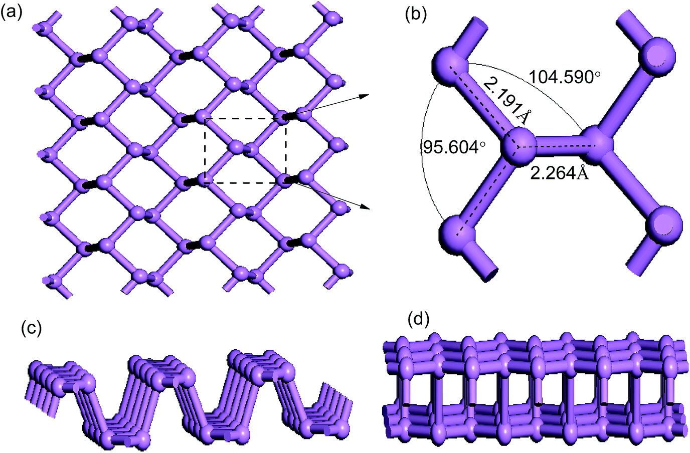 | ||
| Fig. 1 Optimized geometric structures of pristine phosphorene: (a) top view; (b) primitive cell; (c) and (d) side views from the zigzag and armchair directions. | ||
Then, to assess how the substitutional dopants affect the structural properties of phosphorene, the geometric structure of each substitutionally doped phosphorene is optimized. In Fig. 2, (panels a and b) and (panels c and d) show the top and side views of single and co-doped phosphorene, respectively. The phosphorus atoms near the impurity site are labeled by numbers to describe the bond lengths between the dopants and these P atoms below. To quantify the local structure deformation in doped phosphorene caused by the substitutional doping, Table 1 summarizes the calculated bond lengths in the vicinity of the dopants. It is found that, due to the impurity doping, the phosphorus atoms close to the dopant are displaced from their original position and show buckling features. Because of this, noticeable internal distortion surrounding the doping atom is observed.
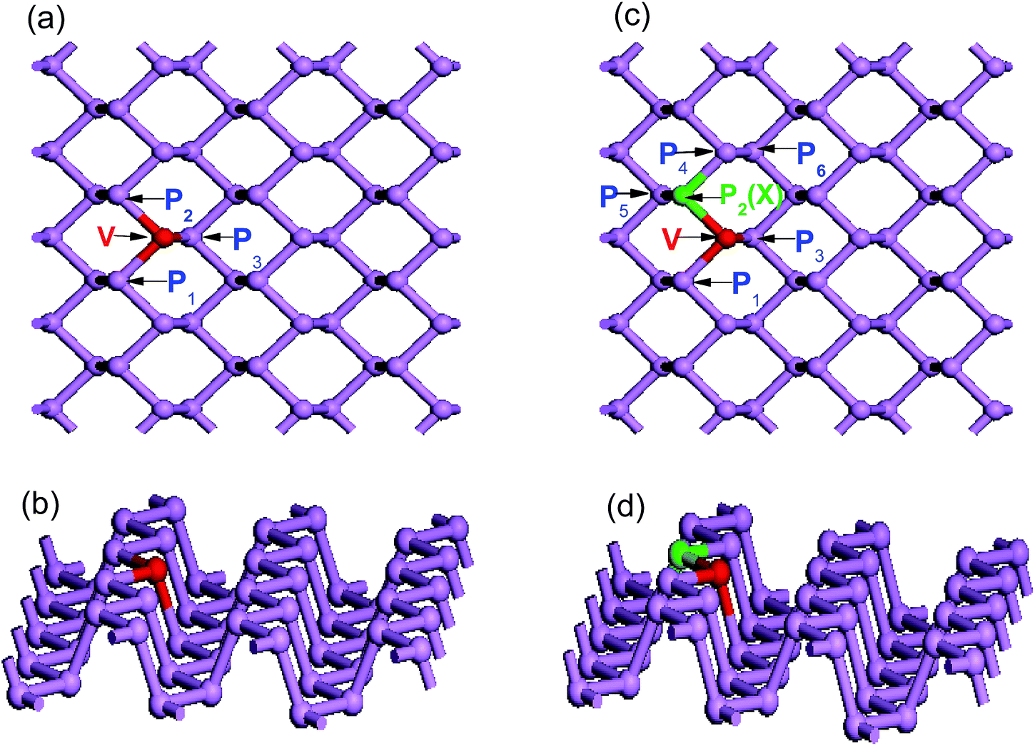 | ||
| Fig. 2 Schematic description of doped phosphorene: (a) top view and; (b) side view of a single V atom doped 4 × 3 × 1 supercell; (c) top view and (d) side view of a V and nonmetallic atom co-doped 4 × 3 × 1 supercell. The violet, red, and green spheres, represent phosphorus, vanadium and nonmetallic atoms, respectively. Phosphorus atom in the phosphorene layer labeled as P2 is replaced by X atoms (X = B, C, N or O). | ||
| Dopant atom (s) | V–P1 (Å) | V–P2 (Å) | V–P3 (Å) |
|---|---|---|---|
| V | 2.417 | 2.417 | 2.315 |
| V–B | 2.384 | 2.015 (P2 = B) | 2.292 |
| V–C | 2.391 | 1.899 (P2 = C) | 2.331 |
| V–N | 2.384 | 1.887 (P2 = N) | 2.396 |
| V–O | 2.459 | 2.150 (P2 = O) | 2.374 |
In the case of single V-doped MBP, the calculated bond lengths (V–P1, V–P2, and V–P3) are 2.417, 2.417 and 2.315 Å, respectively. These calculated values are in good agreement with previous calculations.59 The bond lengths of the intra-planar V–P1 and V–P2 bond lengths are larger than that of the inter-planar V–P3, which indicates that the vanadium atom moves from the top layer to the bottom layer. As discussed above, the single V dopant does not induce significant local lattice distortion. In contrast, from Table 1 we find that V and nonmetallic X (X = B, C, N, and O) atom co-doping induces pronounced local lattice distortion, therefore the values of V–P1, V–X, and V–P3 are not identical. This may be due to the large difference in atomic radii and electronegativity between the P atom and substitutional dopants.
In order to explore the synergistic effect of the two different dopants on the electronic and optical properties of phosphorene, four main possible co-doping models should be considered. Here, we take the V and N atoms as an example to analyze the four different co-doping cases. As shown in Fig. 2(b), besides the fixed V dopant, the N dopant will occupy one of the four possible sites P2, P3, P4, and P6 for the four different cases. And, they are respectively named as the first, the second, the third and the fourth cases in the following analysis. Subsequently, the related stabilities of the four different co-doping cases are discussed by calculating their corresponding formation energies. The co-doped formation energy can be defined as Eform = Etot (V–N) − Etot (MBP) + 2EP − EV − EN, where Etot (V–N) is the total energy of V–N co-doped phosphorene, and Etot (MBP) denotes the total energy of the pure phosphorene supercell. EP, EV and EN represent the energies of the single P, V and N atoms, respectively. It is well known that the smaller the value of the formation energy is, the greater the stability of the structure should be. According to our calculated results, we find that the formation energies of the first and the second cases are −7.902 and −7.988 eV respectively, while those of the third and the fourth cases are −6.616 and −7.109 eV respectively. It is obvious that the former two cases with the smaller formation energies are more stable than the latter two cases. Furthermore, the formation energies of the former two cases have only a little difference, which means both of them should be possible stable structures. However, as shown in Table 1, the bond length of the intra-planar V–N bond in the first case is much shorter than that of the inter-planar V–N bond in the second case. To investigate the synergistic effect of the dopants, we restrict our discussions to the first case only, which has the shorter intra-planar bond and stronger interactions between both doping atoms.
3.2 Electronic properties
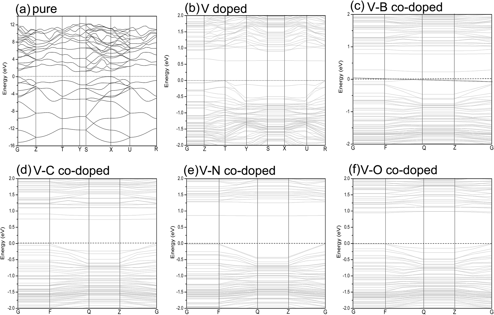 | ||
| Fig. 3 Band structures of pure (a); single V-doped (b); V–B co-doped (c); V–C co-doped (d); V–N co-doped (e); V–O co-doped (f) phosphorene. The horizontal zero line represents the Fermi level. | ||
Fig. 3(b) shows the band structure of single V doped phosphorene. The band structure reveals that the V atom substitutionally doped 2D phosphorene retains a direct band gap of about 0.604 eV. This means that V-doped phosphorene is a semiconductor, which is in qualitative agreement with the recent theoretical result from Yu et al.58 that all Ti-, V-, Cr-, Mn-, Fe-, and Ni-doped black phosphorenes show semiconducting characters. The only difference is that the band gap of V-doped phosphorene calculated by us is larger than that obtained by Yu et al. We suppose that such a difference originates from the neglecting of the strong Coulomb repulsion among V 3d electrons in ref. 58. Besides, via density functional calculations, Hashmi et al.59 also investigated the substitutional doping of phosphorene systems with a series of 3d transition-metal atoms such as Sc, Ti, V, Cr, Mn, Fe, Co, Ni, and Cu. They suggested that most of the transition-metal doped phosphorenes still have a semiconducting band gap, whereas only V- and Fe-doped systems are half-metallic states. As discussed above, there is still a debate on whether V-doped phosphorene is a semiconductor. Because there are no available experimental data, we expect that the electronic properties of V-doped phosphorene will be uncovered by experimental measurement. Therefore, we think that it may be an interesting issue worthy of further study. It can be seen from Fig. 3(b) that a flat impurity state appears just above the Fermi level, which is mainly contributed by the 3d state of the vanadium atom. More detailed analysis with respect to the composition of the energy band will be provided below.
The band structures of V–B (C, N or O) co-doped phosphorene are also investigated to further understand how the electronic structure is affected by different dopants. Fig. 3(c)–(f) represents the band structures of the V–B, V–C, V–N and V–O co-doped systems, respectively. We find that different dopants induce different band structures. The new impurity energy levels introduced by the substitutional dopants have an increasing tendency, as we change the nonmetallic atom from B to O. The band gaps are about 0.327, 0.737, 0.851 and 0.940 eV for V–B, V–C, V–N and V–O co-doped phosphorene, respectively. It is noteworthy that both the mono- and co-doped phosphorene systems retain direct band gap characters. In addition, doping with transition-metal and nonmetallic atoms can make the energy band gap smaller than that of primitive phosphorene by forming impurity states in the band gap. Such results reveal that these dopants can be used to modulate the band gap of phosphorene.
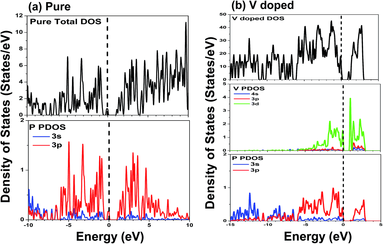 | ||
| Fig. 4 Density of states (DOS) and projected density of states (PDOS) of primitive phosphorene (a); single V atom substitutionally doped phosphorene (b). The Fermi level is labeled by a dash line, and the smearing width is set to be 0.05 eV. | ||
The DOS and PDOS of phosphorene co-doped with vanadium and nonmetallic atoms are depicted in Fig. 5. Comparing Fig. 4(b) with Fig. 5(a), we find that the B atom incorporated into single V-doped phosphorene doesn’t significantly change the distribution of the DOS. Besides, it can also be observed that the highest occupied valence band is derived mainly from the V-3d, P-3p, and B-2p orbitals. Similar to the V–B co-doped case, the valence bands of the other co-doped systems (V–C, V–N and V–O) are mainly attributed to the hybridization between the 3d states of the V atom, the 3p states of the nearest P atoms, and the 2p states of the nonmetallic atom (see Fig. 5(b)–(d)). Further noted from Fig. 5(b)–(d) is that the overlap between the 2p orbitals of the C or N atom and the 3p orbitals of the P atom is obvious, whereas the overlap between the O-2p and P-3p states is relatively unobvious. So this indicates that the interaction between the P-3p and C (N)-2p states is stronger than that between the P-3p and O-2p states, implying that the C (N)–P bonds may possess stronger covalent bonding strength than the O–P bonds. This phenomenon is mainly due to the different electronegativities of the C, N and O atoms. In addition, the lowest conduction bands of the co-doping systems are mainly formed by the 3d states of the vanadium atom.
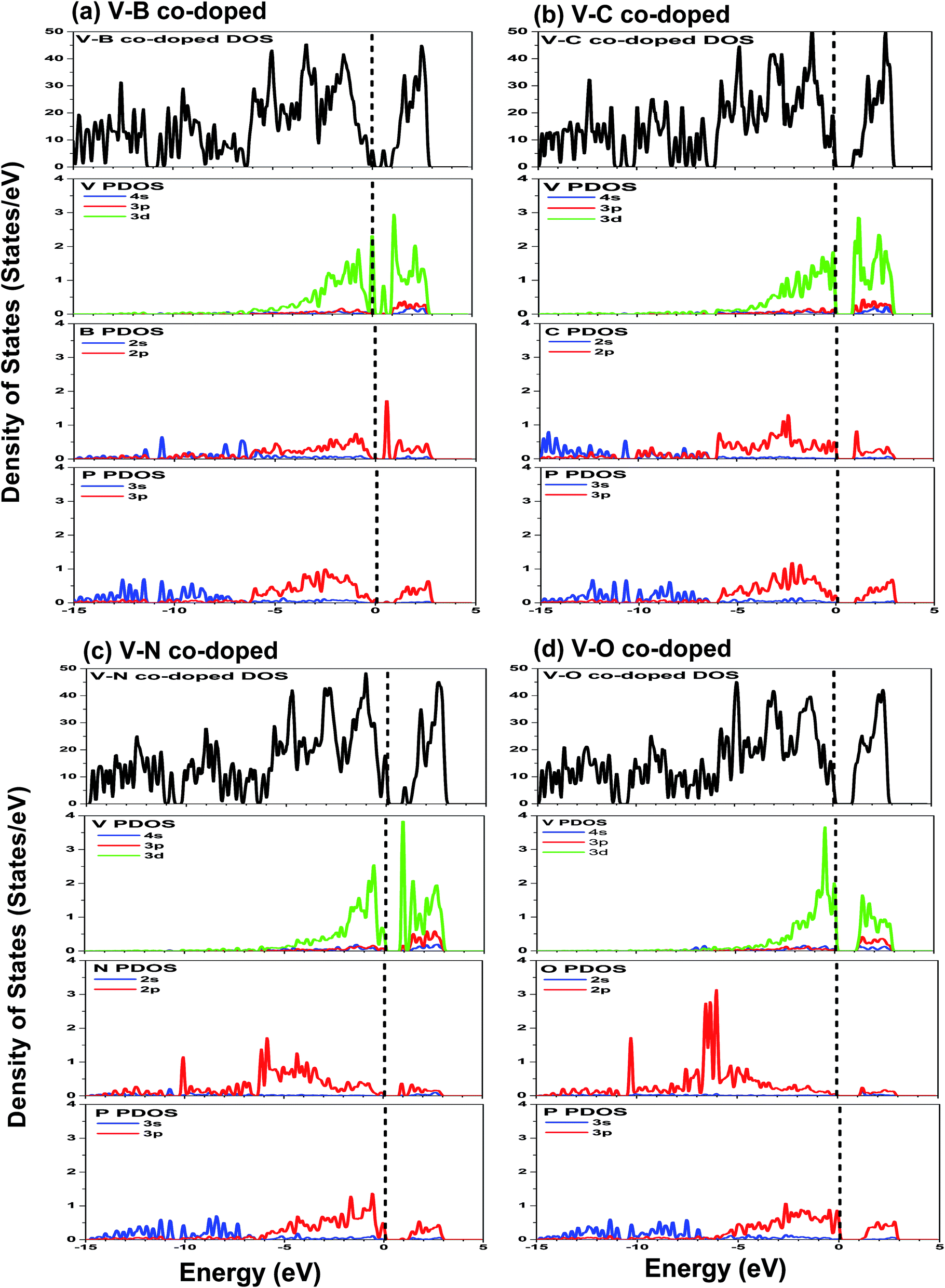 | ||
| Fig. 5 DOS and PDOS of co-doped phosphorene: (a) V–B co-doped; (b) V–C co-doped; (c) V–N co-doped; (d) V–O co-doped. The Fermi level is labeled by a dash line, and the smearing width is set to be 0.05 eV. | ||
| Dopant atom (s) | Bond | Overlap population | Length (Å) |
|---|---|---|---|
| V | V–P1 | 0.36 | 2.417 |
| V–P2 | 0.36 | 2.417 | |
| V–P3 | 0.35 | 2.315 | |
| V–B | V–P1 | 0.44 | 2.384 |
| V–B | −0.01 | 2.015 | |
| V–P3 | 0.35 | 2.292 | |
| B–P4 | 0.95 | 1.864 | |
| B–P5 | 0.81 | 1.877 | |
| V–C | V–P1 | 0.44 | 2.391 |
| V–C | 0.27 | 1.899 | |
| V–P3 | 0.38 | 2.331 | |
| C–P4 | 0.70 | 1.757 | |
| C–P5 | 0.71 | 1.763 | |
| V–N | V–P1 | 0.44 | 2.384 |
| V–N | 0.27 | 1.887 | |
| V–P3 | 0.44 | 2.396 | |
| N–P4 | 0.48 | 1.711 | |
| N–P5 | 0.40 | 1.717 | |
| V–O | V–P1 | 0.38 | 2.459 |
| V–O | 0.14 | 2.150 | |
| V–P3 | 0.38 | 2.374 | |
| O–P4 | 0.25 | 1.707 | |
| O–P5 | 0.11 | 1.822 |
3.3 Optical properties
Here, the optical properties of pure and differently doped MBP are systematically discussed on the basis of the dielectric function. It is well known that the imaginary part of the dielectric function (ε2(ω)) is an effective parameter to measure the optical absorption of materials. The imaginary parts of the dielectric function along three directions for pristine and dopant modified phosphorenes are shown in Fig. 6. Due to the anisotropy of phosphorene along the x, y and z directions, the computed ε2(ω) in the three directions presents different characteristics. As shown in Fig. 6(a)–(c), the ε2(ω) of impurity doped phosphorene shows a distinctive difference from that of pristine phosphorene along the three directions, demonstrating that substitutional dopants have a profound influence on the optical spectra. As a representative system, we discuss the curves of ε2(ω) along the x direction in detail (see Fig. 6(a)), since ε2(ω) along the other two directions can be understood in a similar way. For pure phosphorene, a quite wide absorption band in the region from 1.964 eV to ∼9.0 eV is observed clearly (see the black curve in Fig. 6(a)). The light within such an energy range will be strongly absorbed by the pristine case. In Fig. 6(a), the absorption edge of the pure phosphorene monolayer is ∼1.964 eV, which is in good agreement with the experimental value of the band gap of phosphorene (2 eV).41 After introducing dopants, the absorption edges are shifted to a lower energy range compared with that of pristine phosphorene. That is, individual V atom doping and V–B (C, N, and O) co-doping all make the optical absorption edges generate the redshift phenomenon, which results in the enhancement of the absorption of infrared light in phosphorene. The absorption edges of the V-doped, V–B, V–C, V–N and V–O co-doped systems become 0.708, 0.457, 0.750, 0.805 and 0.959 eV, respectively (see details in the inset of Fig. 6(a)). As is known, the order of the radius size for nonmetallic atoms is O > N > C > B. As the nonmetallic atom is incorporated into V-doped phosphorene, the absorption edge increases as the radius of the nonmetallic atom increases. For the ε2(ω) spectra along the y direction, the absorption edges of primitive and one vanadium atom doped phosphorene are about 2.508 and 1.085 eV, respectively, indicating an obvious redshift phenomenon. Nevertheless, the edges of the co-doped systems are nearly the same as each other about ∼1.433 eV. In addition, the edges of ε2(ω) along the z direction are ∼1.057, 0.617, 0.373, 0.680, 0.736 and 0.903 eV for pure, single V doped, and V–B, V–C, V–N and V–O co-doped phosphorene, respectively. The redshift phenomenon is also obtained along the z direction. It should be noted that the optical absorption edges of all cases along the z direction are consistent with the corresponding energy band gaps mentioned above. In brief, all the doped cases reflect redshift phenomena along the x, y and z directions and all the absorption peaks become weaker.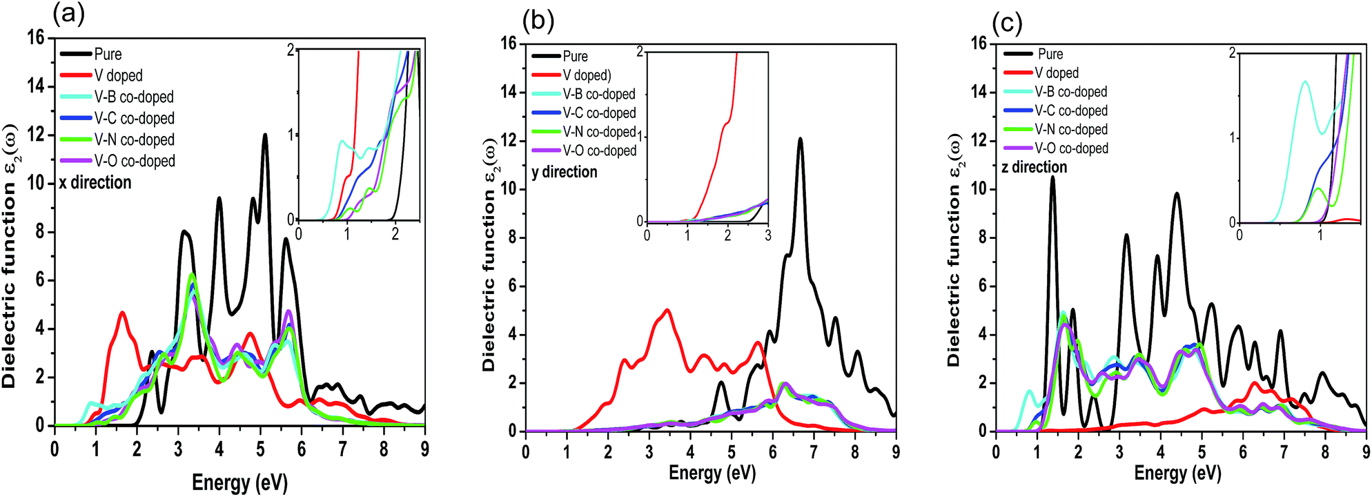 | ||
| Fig. 6 Imaginary parts of the dielectric function versus energy for pristine and substitutional impurity modified phosphorenes along the x (a), y (b), and z (c) directions. | ||
4 Conclusions
In summary, based on the first-principle calculations within the framework of DFT, we carried out a systematic investigation on the geometric, electronic and optical properties of phosphorene with various dopants. This study aimed to identify possible doping strategies for phosphorene. Electronic structures and optical properties of single V atom doped or V–B, V–C, V–N and V–O co-doped phosphorene systems were analyzed and compared to identify the general trends and individual characteristics. According to our calculations, the optimized structural parameters (bond lengths and angles) are in good agreement with previous works. The impurity doping induces local lattice distortion and the detailed local geometric structures are dependent on the specific dopants. One vanadium atom substitutional doping does not induce huge local lattice distortion, while pronounced distortion is induced by V and nonmetallic atom (B, C, N, and O) co-doping.Next, the band structures of all the substituted systems were explored. The results reveal that both one V atom doped and V–B (C, N, O) co-doped phosphorene all exhibit semiconducting behavior but with smaller band gaps than that of the pure case. Doping atoms considered in the present paper decrease the band gap by forming impurity states in the band gap region. The band gap in co-doped phosphorene increases from 0.327 to 0.940 eV as we change the substitutional nonmetal atoms from B to O. Band structure analysis also shows that by introducing nonmetallic atoms into a V-doped single phosphorene sheet, the band gap of dopant modified phosphorene can further increase or decrease, which may broaden the applications of phosphorene in developing nanoelectronics and optoelectronics.
Furthermore, the DOS, PDOS and Mulliken population were analyzed by us explicitly. It was found that V atom doping in phosphorene leads to the formation of V (3d)–P (3p) hybridized states at the top of the valence band. In addition, incorporation of a nonmetallic atom into V-doped phosphorene induces the interaction between the P-3p and 2p states of the nonmetallic atom. Among the doping nonmetallic atoms, the strongest covalent interaction was found between the B and P atoms. Meanwhile, there exists a very weak antibonding (or no bonding) state between the B and V atoms. These fascinating phenomena can be explained by the different electronegativities of the nonmetallic atoms.
Finally, the optical properties of phosphorene with different dopants were studied and compared with the pristine case. As a result, the computed imaginary parts of the dielectric function display different characters along the x, y, and z directions because of the anisotropy of phosphorene which is the origin of the anisotropic physical and mechanical properties. Besides, in the single V doping and V–B (C, N, O) co-doping cases, the optical absorption edges exhibit a distinct redshift phenomenon. Therefore, foreign atom substitutional doping is shown to be an effective way for modulating the electronic and optical properties of phosphorene. We hope that our findings may facilitate wider applications of phosphorene.
Acknowledgements
This work is supported by the Chinese National Science Foundation under Grant No. 21576208. It is also partly supported by the founding from the State Key Laboratory of Separation Membranes and Membrane Processes (Tianjin Polytechnic University). Numerical calculations for this work were carried out on the Parallel Computer Cluster of the School of Materials Science and Engineering at Tianjin Polytechnic University.References
- K. S. Novoselov, A. K. Geim, S. V. Morozov, D. Jiang, Y. Zhang, S. V. Dubonos, I. V. Grigorieva and A. A. Firsov, Science, 2004, 306, 666–669 CrossRef CAS PubMed.
- C. Lee, X. Wei, J. W. Kysar and J. Hone, Science, 2008, 321, 385–388 CrossRef CAS PubMed.
- A. A. Balandin, S. Ghosh, W. Z. Bao, I. Calizo, D. Teweldebrhan, F. Miao and C. N. Lau, Nano Lett., 2008, 8, 902–907 CrossRef CAS PubMed.
- A. H. Castro Neto, F. Guinea, N. M. R. Peres, K. S. Novoselov and A. K. Geim, Rev. Mod. Phys., 2009, 81, 109–162 CrossRef CAS.
- X. Du, I. Skachko, F. Duerr, A. Luican and E. Y. Andrei, Nature, 2009, 462, 192–195 CrossRef CAS PubMed.
- R. Rasuli, A. I. zad and M. M. Ahadian, Nanotechnology, 2010, 21(185503), 1–6 Search PubMed.
- A. H. Castro Neto and K. Novoselov, Rep. Prog. Phys., 2011, 74, 82501–82509 CrossRef.
- A. A. Balandin, Nat. Mater., 2011, 10, 569–581 CrossRef CAS PubMed.
- N. O. Weiss, H. Zhou, L. Liao, Y. Liu, S. Jiang, Y. Huang and X. Duan, Adv. Mater., 2012, 24, 5782–5825 CrossRef CAS PubMed.
- P. Nath, D. Sanyal and D. Jana, Physica E: Low-dimensional Systems and Nanostructures, 2015, 69, 306–315 CrossRef CAS.
- E. S. Reich, Nature, 2014, 506, 19 CrossRef PubMed.
- H. Wang, H. Yuan, S. S. Hong, Y. Li and Y. Cui, Chem. Soc. Rev., 2015, 44, 2664–2680 RSC.
- Q. H. Wang, K. Z. Kourosh, A. Kis, J. N. Coleman and M. S. Strano, Nat. Nanotechnol., 2012, 7, 699–712 CrossRef CAS PubMed.
- M. Chhowalla, H. S. Shin, G. Eda, L. J. Li, K. P. Loh and H. Zhang, Nat. Chem., 2013, 5, 263–275 CrossRef PubMed.
- A. L. Elas, N. Perea-López, A. Castro-Beltrán, A. Berkdemir, R. Lv, S. Feng, A. D. Long, T. Hayashi, Y. A. Kim and M. Endo, ACS Nano, 2013, 7, 5235–5242 CrossRef PubMed.
- K. F. Mak, C. Lee, J. Hone, J. Shan and T. F. Heinz, Phys. Rev. Lett., 2010, 105, 136805 CrossRef PubMed.
- D. Lagarde, L. Bouet, X. Marie, C. R. Zhu, B. L. Liu, T. Amand, P. H. Tan and B. Urbaszek, Phys. Rev. Lett., 2014, 112, 1–4 CrossRef PubMed.
- A. M. Hu, L. L. Wang, W. Z. Xiao, G. Xiao and Q. Y. Rong, Comput. Mater. Sci., 2015, 107, 72–78 CrossRef CAS.
- B. Radisavljevic and A. Kis, Nat. Mater., 2013, 12, 815–820 CrossRef CAS PubMed.
- B. Radisavljevic, A. Radenovic, J. Brivio, V. Giacometti and A. Kis, Nat. Nanotechnol., 2011, 6, 147–150 CrossRef CAS PubMed.
- H. Liu, A. T. Neal, Z. Zhu, Z. Luo, X. Xu, D. Tománek and P. D. Ye, ACS Nano, 2014, 8, 4033–4041 CrossRef CAS PubMed.
- L. Li, Y. Yu, G. J. Ye, Q. Ge, X. Ou, H. Wu, D. Feng, X. H. Chen and Y. Zhang, Nat. Nanotechnol., 2014, 9, 372–377 CrossRef CAS PubMed.
- A. S. Rodin, A. Carvalho and A. H. CastroNeto, Phys. Rev. Lett., 2014, 112, 176801 CrossRef CAS PubMed.
- Z. Zhu and D. Tománek, Phys. Rev. Lett., 2014, 112, 176802 CrossRef PubMed.
- R. Fei and L. Yang, Nano Lett., 2014, 14, 2884–2889 CrossRef CAS PubMed.
- V. Tran, R. Soklaski, Y. Liang and L. Yang, Phys. Rev. B: Condens. Matter Mater. Phys., 2014, 89, 235319 CrossRef.
- X. Peng, Q. Wei and A. Copple, Phys. Rev. B: Condens. Matter Mater. Phys., 2014, 90, 085402 CrossRef.
- F. Xia, H. Wang and Y. Jia, Nat. Commun., 2014, 5, 4458 CAS.
- J. Qiao, X. Kong, Z. X. Hu, F. Yang and W. Ji, Nat. Commun., 2014, 5, 4475 CAS.
- S. P. Koenig, R. A. Doganov, H. Schmidt, A. H. Castro Neto and B. Öezyilmaz, Appl. Phys. Lett., 2014, 104, 103106 CrossRef.
- H. Zheng, J. Zhang, B. Yang, X. Du and Y. Yan, Phys. Chem. Chem. Phys., 2015, 17, 16341–16350 RSC.
- B. Sa, Y. L. Li, J. Qi, R. Ahuja and Z. Sun, J. Phys. Chem. C, 2014, 118, 26560–26568 CAS.
- V. V. Kulish, O. I. Malyi, C. Persson and P. Wu, Phys. Chem. Chem. Phys., 2015, 17, 13921–13928 RSC.
- Y. Xu, J. Dai and X. C. Zeng, J. Phys. Chem. Lett., 2015, 6, 1996–2002 CrossRef CAS PubMed.
- G. Qin, Q. B. Yan, Z. Qin, S. Y. Yue, H. J. Cui, Q. R. Zheng and G. Su, Sci. Rep., 2014, 4, 6946 CrossRef CAS PubMed.
- A. Jain and A. J. H. McGaughey, Sci. Rep., 2014, 5, 8501 CrossRef PubMed.
- Q. Wei and X. Peng, Appl. Phys. Lett., 2014, 104, 251915 CrossRef.
- J. W. Jiang and H. S. Park, J. Phys. D: Appl. Phys., 2014, 47, 385304 CrossRef.
- L. Wang, A. Kutana, X. Zou and B. I. Yakobson, Nanoscale, 2015, 7, 9746–9751 RSC.
- J. Dai and X. C. Zeng, J. Phys. Chem. Lett., 2014, 5, 1289–1293 CrossRef CAS PubMed.
- M. Buscema, D. J. Groenendijk, S. I. Blanter, G. A. Steele, H. S. J. vander Zant and A. C. Gomez, Nano Lett., 2014, 14, 3347–3352 CrossRef CAS PubMed.
- X. Ling, H. Wang, S. Huang, F. Xia and M. S. Dresselhaus, Proc. Natl. Acad. Sci. U. S. A., 2015, 112, 4523–4530 CrossRef CAS PubMed.
- M. Engel, M. Steiner and P. Avouris, Nano Lett., 2014, 14, 6414–6417 CrossRef CAS PubMed.
- C. Zhang, G. Xiang, M. Lan, Z. Tang, L. Deng and X. Zhang, RSC Adv., 2015, 5, 40358–40362 RSC.
- L. Kou, T. Frauenheim and C. Chen, J. Phys. Chem. Lett., 2014, 5, 2675–2681 CrossRef CAS PubMed.
- L. Kou, Y. Ma, S. C. Smith and C. Chen, J. Phys. Chem. Lett., 2015, 6, 1509–1513 CrossRef CAS PubMed.
- X. Sui, C. Si, B. Shao, X. Zou, J. Wu, B. L. Gu and W. Duan, J. Phys. Chem. C, 2015, 119, 10059–10063 CAS.
- T. Hu and J. Hong, J. Phys. Chem. C, 2015, 119, 8199–8207 CAS.
- H. Guo, N. Lu, J. Dai, X. Wu and X. C. Zeng, J. Phys. Chem. C, 2014, 118, 14051–14059 CAS.
- Y. Jing, Q. Tang, P. He, Z. Zhou and P. Shen, Nanotechnology, 2015, 26, 095201 CrossRef CAS PubMed.
- R. Zhang, B. Li and J. Yang, J. Phys. Chem. C, 2015, 119, 2871–2878 CAS.
- M. Buscema, D. J. Groenendijk, G. A. Steele, H. S. J. van der Zant and A. Castellanos-Gomez, Nat. Commun., 2014, 5, 4651 CrossRef CAS PubMed.
- J. Yuan, S. Najmaei, Z. Zhang, J. Zhang, S. Lei, P. M. Ajayan, B. I. Yakobson and J. Lou, ACS Nano, 2015, 9, 555–563 CrossRef CAS PubMed.
- P. Rastogi, S. Kumar, S. Bhowmick, A. Agarwal and Y. S. Chauhan, Effective Doping of Monolayer Phosphorene by Surface Adsorption of Atoms for Electronic and Spintronic Applications, arXiv:1503.04296.
- X. B. Li, P. Guo, T. F. Cao, H. Liu, W. M. Lau and L. M. Liu, Sci. Rep., 2015, 5, 10848 CrossRef CAS PubMed.
- I. Khan and J. Hong, New J. Phys., 2015, 17, 023056 CrossRef.
- W. Yu, Z. Zhu, C. Niu, C. Li, J. H. Cho and Y. Jia, Phys. Chem. Chem. Phys., 2015, 17, 16351–16358 RSC.
- W. Yu, Z. Zhu, C. Y. Niu, C. Li, J. H. Cho and Y. Jia, Dilute magnetic semiconductor and half-metal behaviour mediated by 3d transition-metal doped in black/blue phosphorene, arXiv:1504.01592.
- A. Hashmi and J. Hong, J. Phys. Chem. C, 2015, 119, 9198–9204 CAS.
- L. Kou, C. Chen and S. C. Smith, J. Phys. Chem. Lett., 2015, 6, 2794–2805 CrossRef CAS PubMed.
- S. J. Clark, M. D. Segall, C. J. Pickard, P. J. Hasnip, M. J. Probert, K. Refson and M. C. Payne, Z. Kristallogr., 2005, 220, 567–570 CAS.
- D. Vanderbilt, Phys. Rev. B: Condens. Matter Mater. Phys., 1990, 41, 7892–7895 CrossRef.
- J. P. Perdew, K. Burke and M. Ernzerhof, Phys. Rev. Lett., 1996, 77, 3865–3868 CrossRef CAS PubMed.
- H. J. Monkhorst and J. D. Pack, Phys. Rev. B: Condens. Matter Mater. Phys., 1976, 13, 5188–5192 CrossRef.
- B. G. Pfrommer, M. Ca.te., S. G. Louie and M. L. Cohen, J. Comput. Phys., 1997, 131, 233–240 CrossRef CAS.
- M. D. Krcha and M. J. Janik, Int. J. Quantum Chem., 2014, 114, 8–13 CrossRef CAS.
- S. L. Dudarev, G. A. Botton, S. Y. Savrasov, C. J. Humphreys and A. P. Sutton, Phys. Rev. B: Condens. Matter Mater. Phys., 1998, 57, 1505–1509 CrossRef CAS.
- L. Wang, T. Maxisch and G. Ceder, Phys. Rev. B: Condens. Matter Mater. Phys., 2006, 73, 195107 CrossRef.
- P. Guss, M. E. Foster, B. M. Wong, F. P. Doty, K. Shah, M. R. Squillante, U. Shirwadkar, R. Hawrami, J. Tower and D. Yuan, J. Appl. Phys., 2014, 115, 034908 CrossRef.
- S. Saha, T. P. Sinha and A. Mookerjee, Phys. Rev. B: Condens. Matter Mater. Phys., 2000, 62, 8828–8834 CrossRef CAS.
- P. Y. Yu and M. Cardona, Fundamentals of Semiconductors, Springer Verlag, Berlin, 1996 Search PubMed.
- R. S. Mulliken, J. Chem. Phys., 1955, 23, 1833–1840 CrossRef CAS.
- M. D. Segall, C. J. Pickard, R. Shah and M. C. Payne, Phys. Rev. B: Condens. Matter Mater. Phys., 1996, 54, 16317–16320 CrossRef CAS.
| This journal is © The Royal Society of Chemistry 2016 |