DOI:
10.1039/C5RA21731H
(Paper)
RSC Adv., 2016,
6, 4170-4182
Novel synthesis process for solar-light-active porous carbon-doped CuO nanoribbon and its photocatalytic application for the degradation of an organic dye
Received
18th October 2015
, Accepted 17th December 2015
First published on 22nd December 2015
Abstract
A simple, one-step novel solution process was developed for the synthesis of carbon-doped CuO (C-CuO) nanoribbons without the use of a catalyst, template, substrate, or costly instrumentation at room temperature. The precursor materials used were converted into C-CuO nanoribbons in ethanol (95%) at high concentrations (4.37 mg mL−1) as a colloidal solution with very high dispersion stability. The simplicity, reaction time, production cost, production yield, and environmental friendliness of this process make it suitable for the large-scale industrial production of C-CuO nanoribbons. The prepared nanoribbon is also separable and redispersible in other organic solvents. The dispersibility in multiple solvents highlights its versatility as a platform for depositing other nanomaterials on its surface in organic media to improve its additional properties as a candidate for other applications. Its three-dimensional surface morphology was characterized, which suggested that the prepared C-CuO nanoribbon was highly porous. Free-standing C-CuO nanoribbon films were also prepared using a simple process. The prepared film of porous C-CuO nanoribbon exhibited excellent light absorption ability in the range from visible to near-IR light with higher intensity. The superior light absorption properties of the C-CuO nanoribbons were utilized in a photocatalyst to decompose an organic dye in visible light. The degradation of the organic dye (96.64%), recycling performance (93.94%), number of cycles (24), and degradation time (120 min) highlight its potential as a very good photocatalyst.
1. Introduction
Owing to their effective transport of electrons and excitons through the smallest distances, one-dimensional (1D) semiconductor and metal nanomaterials are considered crucial structural constituents of electronic, magnetic and photonic devices because of their characteristic anisotropy. Their unique properties can be harnessed for the design and fabrication of nanosensors,1,2 switches,2 nanolasers,3 and transistors.4 Many possible applications of 1D nanomaterials require the formation of well-aligned arrays to increase their anisotropy and satisfy the criteria of device design. Copper oxide 1D semiconductor materials, such as CuO nanowires (or nanoribbons), have attracted tremendous attention because of their wide range of applications such as in bioanodes,5 CO oxidation,6 supercapacitors,7 hydrogen production by the reduction of water,8,9 H2O2 degradation,10 sodium-ion batteries,11 and photon sensing.12 However, in most cases, a catalyst, substrate, template, high temperatures, and multiple chemicals and steps are involved in the synthesis of CuO nanoribbons. For example, substrate (copper, silicon, polycarbonate or other substrate) surfaces5,6,8–18 are used to grow CuO, Cu2O or Cu(OH)2 nanowires. In addition, in many cases, the substrates are treated in acids and other solvents for cleaning and to make them active for the growth of nanowires.5,9,14 High temperatures (400–700 °C)5,6,8,14,16 are used in some cases for the oxidation of the copper substrate but smooth homogeneous nanowires with a high aspect ratio have not been obtained.8,12 The nanowires prepared by these substrate-based processes are applicable to specific applications. To be usable in flexible applications, nanowires need to be separated from the substrate surface, which is time-consuming and requires different chemicals and multiple steps.10 Moreover, no procedure has been reported for separating grown nanowires from the substrate.5,6,8,9,11–18 During the separation period, there is a high likelihood that the nanowires would be damaged. Indeed, separating nanowires from a substrate is quite difficult. Very few studies have been conducted to prepare substrate-free CuO nanoribbons in solution over the past few years. Among these, only two processes have been considered to be significant flexible methods for fabricating well-defined smooth copper oxide nanowires19,20 in solution. Among these two processes, one method requires relatively high temperatures (140–250 °C), reductants (2,5-dimethoxyaniline, o-anisidine or pyrrole), multiple-step reactions, and a long time (10–15 h) to synthesize CuO nanowires.19 The reductant gives rise to another problem with respect to its polymerization in the CuO nanowire solution during the synthesis process. The produced polymer is deposited on the surface of nanowires as an outer shell layer, which has some negative impacts depending on the type of application. For example, in some cases, other conducting or semiconducting metals or metal oxides may be required for direct deposition on the surfaces of synthesized CuO nanowires to improve their electrical, optical and electrochemical properties. On the other hand, the polymer acts as a barrier to the direct deposition of other materials on the surface of CuO nanowires because it acts as a shell layer. Furthermore, the prepared nanowire should be dispersible in a solution of other materials to be usable as a platform for the deposition of other nanoparticles in solution. A CuO nanoribbon with a deposited polymer is not dispersed easily in organic solvents. In the other process,20 polyethylene glycol is used as a surfactant, NaOH is used as a catalyst and hydrazine hydrate (N2H4·H2O) is used as a reducing agent for the synthesis of CuO nanowires from Cu(OH)2. Actually, this process is comparatively better but requires multiple steps, which take time, needs multiple reagents that leave impurities in the CuO matrix, causes environmental pollution and has high production cost. Therefore, neither of these processes is usable as a low-cost novel process for the synthesis of versatile CuO nanoribbons on a large scale. In fact, the novelty of a material depends on its versatility, dispersibility in other solvents at high concentrations and a simple synthesis process, which should be free from any barrier, such as dependency on a substrate and complexity.
In this study, carbon-doped CuO (C-CuO) nanoribbons were prepared using a single-step, catalyst-free, low-cost, and facile process that enables the large-scale industrial production of C-CuO nanoribbons without the assistance of any substrate at room temperature. The prepared nanoribbons exhibited a very low thickness (2.5–4.0 nm) and narrow band gap (1.31 eV). Free-standing C-CuO nanoribbon films were also prepared using a very simple drop-drying process from the as-prepared solution of C-CuO nanoribbons without the use of any further instruments, solvents and techniques. This is the first time that substrate-free CuO nanoribbons have been synthesized via a solution process that can allow industrial-scale production. The C-CuO nanoribbons displayed excellent absorption capability for visible and near-IR light (400–1665 nm). They were also used as a photocatalyst under sunlight to decompose an organic dye. Their performance in photocatalytic degradation and recycling highlight them as a very good photocatalyst that is stable against photocorrosion under sunlight for decomposing the organic dye methylene blue (MB).
2. Experimental work
2.1 Chemicals and instruments
Chemicals. Copper(II) acetate (98%, Sigma Aldrich), ethanol (absolute, 99.8%, Sigma Aldrich), and ethanol (95%, Duksan, Korea) were used.
Instruments. Structural characterization was conducted using field emission scanning electron microscopy (FESEM, Nova, S-4800, Hitachi, Japan) and FE-TEM (Tecnai G2 F2O S-TWIN, FEI Company, USA). Spectroscopic and crystallographic characterization were carried out by Raman spectroscopy (Horiba Jobin Yvon, LabRAM HR, laser 514.54 nm, USA) and X-ray diffraction (XRD, thin film, MPD, PANalytical), respective. Optical properties were measured by ultraviolet/visible/near infrared (UV/vis/NIR, Cary-5000, Agilent) spectroscopy.
2.2 C-CuO nanoribbon
A 400 mg sample of copper acetate was placed in a glass vial containing 40 mL ethanol (95%, general grade). Bath sonication was performed at room temperature to achieve dissolution. The prepared clear 10 mg mL−1 solution (Fig. 1a, Scheme A) of copper acetate was further bath sonicated continuously to obtain highly concentrated C-CuO nanoribbons with a light blue color (Fig. 1b, Scheme A) from a clear teal (deep blue-green) solution (Fig. 1a). In general, it took 2 h to produce the complete C-CuO nanoribbons from the copper acetate solution. All the C-CuO nanoribbons were floating in ethanol and were well dispersed. A similar experiment was conducted using pure ethanol (absolute, 99.8%, Scheme B) as a solvent for copper acetate to obtain a highly concentrated light blue solution, but no color change was observed (Fig. 1f, Scheme B). Therefore, sonication was continued for up to 12 h but no variation in color was observed and no reaction took place. This shows that C-CuO nanoribbons are not prepared in pure ethanol.
 |
| | Fig. 1 Scheme (A) schematic diagram of C-CuO nanoribbon and its film preparation in general grade ethanol: (a) copper acetate solution (10 mg mL−1) in general grade ethanol, (b) C-CuO nanoribbon solution (4.37 mg mL−1) in ethanol, (c) C-CuO nanoribbon film prepared on paper, (d) technique for the separation of C-CuO nanoribbon film from paper. Scheme (B) schematic diagram showing that absolute ethanol is not effective for the synthesis of C-CuO nanoribbons: (e) copper acetate solution in absolute ethanol, (f) after 12 h sonication, no color change is observed. | |
2.3 Free-standing C-CuO nanoribbon film
A highly concentrated light blue colloid of C-CuO nanoribbons (Fig. 1b) was poured onto white paper (writing paper) and spread out homogenously by slightly shaking the paper. The paper was allowed to dry for 1 h at room temperature (25 °C). For quick drying, some tissue paper was placed under the writing paper, which decreased the drying time by quickly absorbing the ethanol solvent. After drying, the C-CuO nanoribbon film layer deposited on the paper (Fig. 1c) was peeled easily by folding the supporting paper in an outward direction (Fig. 1d). The peeled free-standing film was further dried at 80 °C for 2 h to evaporate the remaining water and ethanol from the film.
2.4 Photocatalytic experiments
The as-prepared C-CuO nanoribbon solution in ethanol (4.37 mg mL−1) was centrifuged at 10![[thin space (1/6-em)]](https://www.rsc.org/images/entities/char_2009.gif) 000 rpm for 1 h and the bottom solution was collected. The resulting bottom solution was diluted to 10 mg mL−1 and 13 mL (130 mg) of it was added to 100 mL of a 7.9 × 10⁻⁴ M solution of MB in water. The solution was sonicated for 5 min in the dark and allowed to settle for 2 h to achieve adsorption/desorption equilibrium. The photocatalytic degradation of MB was carried out in ambient conditions under direct sunlight from 10 am to 12 pm. The outside temperature was 28 to 35 °C. A UV light cutoff filter at 420 nm was used over the reaction bottle to block UV light from participating in the photocatalysis reaction. The mixture was sampled continuously at intervals of 20 min from under the cutoff filter glass and centrifuged for 10 min in the dark to discard any sediment. UV/vis absorption spectra were recorded of all the photocatalysis samples collected at different times. The recycling performance of the C-CuO nanoribbons was measured by collecting the precipitate of the centrifuged products, which was washed with DI water, dried, and used directly to determine the recycling performance for up to 24 cycles.
000 rpm for 1 h and the bottom solution was collected. The resulting bottom solution was diluted to 10 mg mL−1 and 13 mL (130 mg) of it was added to 100 mL of a 7.9 × 10⁻⁴ M solution of MB in water. The solution was sonicated for 5 min in the dark and allowed to settle for 2 h to achieve adsorption/desorption equilibrium. The photocatalytic degradation of MB was carried out in ambient conditions under direct sunlight from 10 am to 12 pm. The outside temperature was 28 to 35 °C. A UV light cutoff filter at 420 nm was used over the reaction bottle to block UV light from participating in the photocatalysis reaction. The mixture was sampled continuously at intervals of 20 min from under the cutoff filter glass and centrifuged for 10 min in the dark to discard any sediment. UV/vis absorption spectra were recorded of all the photocatalysis samples collected at different times. The recycling performance of the C-CuO nanoribbons was measured by collecting the precipitate of the centrifuged products, which was washed with DI water, dried, and used directly to determine the recycling performance for up to 24 cycles.
3. Results and discussion
3.1 Synthesis mechanism for C-CuO nanoribbons
| |
 | (1) |
| |
 | (2) |
| |
 | (3) |
| |
 | (4) |
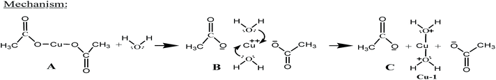
As per the experimental part of the synthesis, general grade alcohol (95%) was useful for synthesizing C-CuO nanoribbons (reaction (2)) and absolute alcohol was not useful for the preparation of C-CuO nanoribbons (reaction (1)). Usually, general grade alcohol contains water (H2O) and absolute alcohol contains no water. Because general grade alcohol was effective for preparing C-CuO nanoribbons, thus it is possible that H2O molecules in alcohol (95%) played a significant role in the synthesis of C-CuO nanoribbons. On the basis of this practical observation, we proposed a reaction mechanism, which shows how water (H2O) molecules played an important role in the synthesis of C-CuO nanoribbons. Reaction (2) shows the sonication of Cu(CH3COO)2 solution in CH3CH2OH + H2O. First, Cu(CH3COO)2 salt is dissolved (reaction (3)) in H2O of alcohol (general grade, CH3CH2OH + H2O) as CH3COO− and Cu2+ ions (B), in which a Cu2+ ion is surrounded by H2O molecules (B) to produce the product Cu-1. Subsequently, Cu-1 produces the product Cu-2 by losing two protons (D, reaction (4)) and alcohol produces a positively charged +OH2 group (E, reaction (4)) from an OH group by capturing a proton at the O atom of its OH group. Finally, the product C-CuO nanoribbon (F) is produced from the product Cu-2 by dehydration, as shown in the last step (F) of reaction (4). Here, a positively charged alcohol also gets attached to an acetate ion through its CH2 carbon, by losing one molecule of water.
3.2 Characterization of C-CuO nanoribbons
The prepared highly concentrated light blue C-CuO product in ethanol was placed on a silicon wafer and dried to obtain SEM and AFM images. SEM (Fig. 2a) reveals a large amount of ribbon-shaped C-CuO material on the silicon wafer. High-resolution SEM (Fig. 2b) of the C-CuO material shows a clear smooth ribbon-like shape. Fig. 2a shows that the average length of C-CuO nanoribbons is about 5 μm. Fig. 2b and c show an average width of 150 nm. Thus, the average aspect ratio (length:width) of the C-CuO nanoribbons is 100:3. TEM (Fig. 2c) also shows clear smooth C-CuO nanoribbons. A high-resolution TEM image (Fig. 2d) taken from the rectangular area of Fig. 2c reveals some crystalline parts of the C-CuO nanoribbon. AFM images (Fig. 2e) were obtained to confirm the ribbon shape of C-CuO and its thickness, which revealed a smooth ribbon-shaped structure. Fig. 2f and g show that ribbons 1 and 2 have thicknesses of 3 and 2.5 nm, respectively. Ribbon 2 is thicker (4 nm) at the position marked by arrows on the solid line owing to the downward bending of the supporting ribbon 1. If ribbon 2 is considered to be the front ribbon, the supporting ribbon would be ribbon 1 (marked by the dotted arrow). Ribbon 2 rests on ribbon 1 and ribbon 1 rests on ribbon 3, which is clearly seen in a 3D AFM image (Fig. 3b). The AFM image (Fig. 2e) is shown in Fig. 3a. Its corresponding 3D image is also shown in Fig. 3b to depict the 3D morphology of the C-CuO nanoribbon. The 3D image (Fig. 3b) clearly reveals a ribbon-shaped morphology and its assembly pattern. The image also shows a well-decorated rough surface (crest) on every nanoribbon. High-resolution AFM images (Fig. 3c and d) in the dotted large and small rectangular areas, respectively, were obtained to better understand the crest pattern of the CuO nanoparticles in the ribbon. Both images display a porous morphology and well-organized arrangement of CuO nanoparticles in the ribbon. High-resolution 3D AFM (Fig. 3e) shows a real view of the porous morphology of the ribbon. For instance, the AFM image in Fig. 3c clearly shows that many pores are available in the C-CuO nanoribbon. Pores are clearly marked in the high-resolution AFM image of the C-CuO nanoribbon (Fig. 3d) and in the 3D AFM image (Fig. 3e) by round dotted circles. The total area of Fig. 3d is 180 nm × 200 nm and the total number of pores is around 11. The sizes of pores were also measured from Fig. 3d and e, and these were about 20–50 nm. In addition, an AFM image (Fig. 3d) was converted into curves (Fig. 3g), which clearly show the pore diameter. For clear identification, three lines were drawn along the direction of the peaks and these are displayed separately in Fig. 3h. Fig. 3h reveals that the diameter of pore initiation and actual pore size is about 40 nm. In addition, the AFM palette setting image (Fig. 3f) obtained from Fig. 3d shows the crest, rising and falling actions of the CuO nanoparticles in a ribbon. One crest position is marked with an arrow in Fig. 3d and the same position is shown in Fig. 3f by an arrow. A few pore positions are marked by (i), (ii), (iii), (iv), (v), and (vi) in Fig. 3f and their corresponding positions are also shown in Fig. 3d.
 |
| | Fig. 2 SEM and AFM images: (a) SEM image of C-CuO nanoribbon, (b) high-resolution SEM image of C-CuO nanoribbon, (c) TEM image of C-CuO nanoribbon, (d) HR-TEM image of C-CuO nanoribbon, (e) AFM image of C-CuO nanoribbon, (f) thickness of C-CuO nanoribbon-1, and (g) thickness of ribbon 2. | |
 |
| | Fig. 3 3D morphology of C-CuO nanoribbon: (a) AFM image of C-CuO nanoribbon, (b) 3D AFM image of C-CuO nanoribbon obtained from (a), (c) high-resolution AFM image obtained from the large rectangular marked area, (d) high-resolution AFM image obtained from the small rectangular area of (a), (e) 3D AFM image of the smaller area, (f) AFM palette setting image obtained from (d), (g) conversion of (d) into curves, (h) lines drawn along the direction of the peaks in (g) are shown here separately. | |
All the XRD peaks (Fig. 4a) were assigned to the monoclinic phase of CuO, which is in good agreement with the JCPDS (05-0661).21,22 The major peaks at 2θ = 35.45° and 37.73° were indexed to the (−111)/(002) and (111)/(200) planes, respectively.22 A broad band peak is observed at the 2θ = 24.81° position, which is the characteristic peak of the (002) plane of carbon materials. This peak indicates that carbon is present in the C-CuO nanoribbon. During the synthesis process, carbon was incorporated in the nanoribbon structure and possibly played a significant role in the formation of the nanoribbon structure. The pristine graphitic carbon peak is generally found at 2θ = ∼25°, but in this case, it is found at a higher d-spacing position. The higher d-spacing can have two explanations. One is the low crystallinity of carbon and the other is the interactions of CuO nanoparticles with carbon.
 |
| | Fig. 4 XRD, XPS and Raman spectra: (a) XRD pattern of C-CuO nanoribbon, (b) Cu 2p XPS spectrum of C-CuO nanoribbon, (c) C 1s XPS spectrum of C-CuO nanoribbon, (d) O 1s XPS spectrum of C-CuO nanoribbon and (e) Raman spectrum of C-CuO nanoribbon. | |
The Cu 2p XPS spectrum (Fig. 4b) was recorded to examine the valency of Cu, its defects and other properties of the C-CuO nanoribbons. Two distinctive peaks with binding energies of 933.88 eV and 954.18 eV for Cu 2p3/2 and Cu 2p1/2, respectively, were observed, which corresponded to Cu(II) oxide.23 Two new peaks as satellite peaks at binding energies of 942.38 and 962.38 eV were observed.24 The deconvoluted curve of the core-level C 1s XPS spectrum (Fig. 4c) revealed several components at 284.61, 285.97, 286.66, and 288.68 eV, which were assigned to C![[double bond, length as m-dash]](https://www.rsc.org/images/entities/char_e001.gif) C bonds of sp2 carbon, C–C bonds of sp3 amorphous carbon, C–O–C, and (CO)O, respectively.25 From these C 1s core-level peaks, it was found that the C-CuO nanoribbon comprises carbon containing different functional groups. This might have been due to chemical bonding to Cu in CuO, which was also predicted by XRD. The peak positions were shifted slightly due to interactions with CuO or because of chemical bonding. The peak with a position at a very low energy, 282.8 eV, was assigned to a chemical bond between Cu and C, such as Cu-C.26,27 The O 1s peaks (Fig. 4d) were deconvoluted into two peaks located at 530.49 and 531.82 eV, which are associated with the lattice oxygen of CuO and surface-adsorbed oxygen species (OH groups), respectively.28 The original O 1s curve and the sum of the deconvoluted curves were matched together and are shown in Fig. 4d (the upper curves). The peaks were shifted slightly owing to the in situ incorporation of carbon in the nanoribbon structure of CuO.
C bonds of sp2 carbon, C–C bonds of sp3 amorphous carbon, C–O–C, and (CO)O, respectively.25 From these C 1s core-level peaks, it was found that the C-CuO nanoribbon comprises carbon containing different functional groups. This might have been due to chemical bonding to Cu in CuO, which was also predicted by XRD. The peak positions were shifted slightly due to interactions with CuO or because of chemical bonding. The peak with a position at a very low energy, 282.8 eV, was assigned to a chemical bond between Cu and C, such as Cu-C.26,27 The O 1s peaks (Fig. 4d) were deconvoluted into two peaks located at 530.49 and 531.82 eV, which are associated with the lattice oxygen of CuO and surface-adsorbed oxygen species (OH groups), respectively.28 The original O 1s curve and the sum of the deconvoluted curves were matched together and are shown in Fig. 4d (the upper curves). The peaks were shifted slightly owing to the in situ incorporation of carbon in the nanoribbon structure of CuO.
For further investigation, the Raman spectrum of the C-CuO nanoribbon was also examined. The Raman spectrum (Fig. 4e) reveals two peaks located at 296.85 (Ag) and 616.06 (Bg) cm−1, which are characteristic of CuO.7 The peaks at 405.19 and 484.42 cm−1 are assignable to 4Γ12− and Γ25+ peaks,29 respectively, of Cu2O. These peaks (405.19 and 484.42 cm−1) show that the prepared C-CuO nanoribbon contains little Cu2O. Both these peaks (4Γ12− and Γ25+) were shifted slightly to a lower-frequency position due to the incorporation of carbon into the CuO nanoribbon. The peaks at 1345.9, 1574.1 and 2678.1 cm−1 are the characteristic D, G and 2D band peaks of carbon. The D band at the 1345.9 cm−1 position indicates that defects are available in the carbon structure, which might explain some of the functional groups in carbon; this was also confirmed by the XPS C 1s core-level spectrum (Fig. 4c).
3.3 Dispersion capability
We separated C-CuO nanoribbon from ethanol solvent by centrifugation and then redispersed it in N-methyl-2-pyrrolidone (NMP) and dimethylformamide (DMF) to study its dispersion capability and stability. In both solvents, C-CuO nanoribbon exhibited very high dispersion capability (4.5 mg mL−1) and stability, as in ethanol (4.37 mg mL−1). Therefore, this solution with very high concentration can be used for the deposition of any metal nanoparticles or semiconductor nanoparticles on the surfaces of C-CuO nanoribbon by flexible organic media. We also studied the deposition capabilities of a colloid with very high concentration on other substrate surfaces (i.e., quartz glass, silicon wafer, FTO, ITO, mica, etc.) for use as a candidate for other applications. It exhibited good deposition or self-assembly capabilities on the above-mentioned substrate surfaces. In addition, for making a polymer-semiconductor composite, a homogeneous dispersion of the semiconductor with high concentration in an organic solvent is very important because in situ polymerization can be carried out in this homogeneous solution with high concentration and the semiconductor can be well dispersed in the polymer matrix with extensive interactions to improve the optical and mechanical properties of the polymer. Thus, our colloidal solution of C-CuO nanoribbon (4.37 mg mL−1) shows high potential as a filler for making polymer–CuO composites.
3.4 C-CuO nanoribbon film and its optical properties
To investigate the light absorbance properties of the C-CuO nanoribbon, a C-CuO nanoribbon film (Fig. 5a) was prepared using a very simple process without using special instrumentation, as discussed in the Experimental section. Fig. 5b shows a low-resolution SEM image of the free-standing film. To clearly display the pattern and structure of a small area of the free-standing film, Fig. 5c was obtained from the rectangular dotted area of Fig. 5b. Fig. 5d was also obtained from the rectangular dotted area of Fig. 5c. Many C-CuO ribbons are observed in Fig. 5d. Fig. 5e and f show high-resolution SEM images of the rectangular marked areas of Fig. 5d and e, respectively. They (Fig. 5e and f) show a more clear view of the C-CuO nanoribbons.
 |
| | Fig. 5 C-CuO nanoribbon free-standing film, photograph and SEM images: (a) photograph of C-CuO nanoribbon free-standing film, (b) SEM image of the C-CuO nanoribbon film, (c) SEM image of the C-CuO nanoribbon film obtained from the rectangular area of (b), (d) SEM image of the C-CuO nanoribbon film obtained from the rectangular area of (c), (e) SEM image of the marked rectangular area of (d), and (f) high-resolution SEM image obtained from the rectangular area of (e). | |
A UV-visible near IR spectrum of the C-CuO nanoribbon film was recorded (Fig. 6a). The film exhibited good light absorption properties from the visible to the near-IR region (400–1675 nm). The light absorption intensity and range (400–1675 nm) of the C-CuO nanoribbon film are higher than those of other nanoribbon/nanowire or nanoparticle composites19,30–35 of CuO or Cu2O. A high-intensity broad band absorption peak was observed at 625 nm. The band gap of the as-prepared C-CuO nanoribbon can be calculated (Fig. 6b) using eqn (1),36 where Eg is the band gap energy, hν is the photon energy, A is the relevant transition characteristic parameter, and α = 1/2 or 2 for the direct or indirect transition between the valence band and the conduction band, respectively.
 |
| | Fig. 6 Light absorption, band gap and photodegradation: (a) UV-visible-NIR absorbance curve of the C-CuO nanoribbon film, (b) curve of (αhν)2 vs. photon energy (eV) for calculating the band gap of the C-CuO nanoribbon, (c) photodegradation curves for different degradation times, (d) curve of degradation rate vs. reaction time, (e) absorbance curves of photodegraded solution of MB after 6, 12, 18, and 24 cycles and (f) curve of degradation rate vs. cycle number. | |
Considering the direct transition, Fig. 6b shows a curve of (αhν)2 vs. photon energy (eV);37,38 a direct band gap of 1.31 eV was measured for the C-CuO nanoribbon. Cu participated in chemical bonding (i.e., Cu–O–C, Cu–C),39 as in the case of other metal oxides,37,40 via a functional group of a carbon atom at a defect site. Possibly, a defect was created in the CuO matrix due to the direct (Cu–C) or indirect (Cu–O–C) chemical bonding of carbon with Cu and eventually the band gap decreased. The narrower band gap of the C-CuO nanoribbon can also explain the greater absorption of light at a longer wavelength.
3.5 Photocatalytic performance
Fig. 6c shows the decomposition of MB in the presence of C-CuO nanoribbon after 0, 20, 40, 60, 80, 100, and 120 min of photocatalytic reaction under direct sunlight in an outdoor environment. A UV cut-off filter glass (65CGA-420 CG495, 50% T point at 420.70 nm, Newport) at 420 nm was used over the reaction vessel in the outdoor environment to block UV light from natural sunlight in the photocatalytic reaction. The decomposition (Fig. 6d) of MB in the presence of C-CuO occurred rapidly for the first 20 min of the reaction. However, the degradation rate was comparatively slower from the 40th to the 120th min of the reaction. The rate of degradation of MB was calculated using eqn (2).38,41,42 Here, η = the degradation rate, A0 = the absorbance after zero decomposition time and At = the absorbance at a decomposition reaction time of t.| |
 | (6) |
Fig. 6e shows the absorbance curve for the recycling performance of C-CuO nanoribbon for up to 24 cycles. Every photocatalysis reaction was carried out for 120 min in the presence of C-CuO. The C-CuO nanoribbons were collected by filtration followed by washing and drying. After the separation of the C-CuO nanoribbon by filtration, the filtered MB solution was used to record UV-visible spectra to measure the absorbance and calculate the degradation rate. The absorbance curves of photocatalytically degraded MB solution after the 1st, 6th, 12th, 18th and 24th cycles (Fig. 6e) were used directly to calculate the degradation rate as a percentage. The degradation rates of MB solution after the 1st, 6th, 12th, 18th and 24th cycles in the presence of C-CuO nanoribbon were 98.1%, 96.3%, 95.9%, 95.6% and 95.4% (Fig. 6f). In addition, for the measurement of the self-degradation rate of MB, a control reaction was carried out without a photocatalyst and the relevant curve is shown in Fig. 6c. From the absorbance in that curve, the self-degradation rate (1.46%) was calculated using eqn (2). Thus, the actual degradation by C-CuO nanoribbon was calculated by deducting self-degradation (1.46%) from the degradation in the first cycle. For example, the degradation rates in the first cycle and control reaction (self-degradation) were 98.1% and 1.46%, respectively. Therefore, the actual degradation rate was 96.64% (98.1% − 1.46% = 96.64%). Similarly, the actual degradation rate of MB after the 24th cycle was 93.94%. This means there was only a 2.7% (96.64% − 93.94% = 2.7%) decrease in the degradation rate after 24 cycles. The very high actual degradation rate (93.94%) for C-CuO nanoribbons that had been recycled 24 times suggests that the prepared nanoribbons are highly stable against photocorrosion. The recycling performance curve (Fig. 6f) clearly shows a rapid decrease in degradation in the first 6 cycles that became slower after 6–12, 12–18 and 18–24 cycles. The excellent photocatalysis performance was achieved not because of a single reason, but owing to the combination of the narrow band gap of C-CuO nanoribbon, the participation of carbon as a platform for electron transfer in C-CuO nanoribbon, oxygen vacancy defects in C-CuO nanoribbon and the porous structure of C-CuO nanoribbon. For example, carbon materials (carbon nanosheets, graphene or other forms of carbon) can increase the electrical conductivity of semiconductive materials. In addition, carbon materials can play a significant role in improving the photoactivity of photocatalysts as a reservoir of photoelectrons.43 Owing to the high electrical conductivity of carbon materials, they can transfer electrons rapidly from the valence band of a semiconductor to carbon and enhance the separation efficiency of photo-generated electron–hole pairs by acting as an inhibitor of recombination.43 Because the interface of the C-CuO system was strongly bridged by chemical bonds, which were described by XPS analysis (Fig. 4c and d), the migration of electrons to the carbon surface from the CuO nanoribbon was more convenient as a result of good interfacial interaction or bridging chemical bonds at the interface. As a result, the lifetime of photogenerated charge carriers was increased by decreasing the recombination rate.43–47 It was also discovered that carbon materials enhance the dye adsorption capability of a semiconductor as a composite and this increase in dye adsorption is helpful for the additional degradation of dyes.44,47 Furthermore, 2D carbon materials significantly improve the light absorption properties of semiconductor materials by controlling their band gap,45 which is also crucial for developing photocatalytic performance.
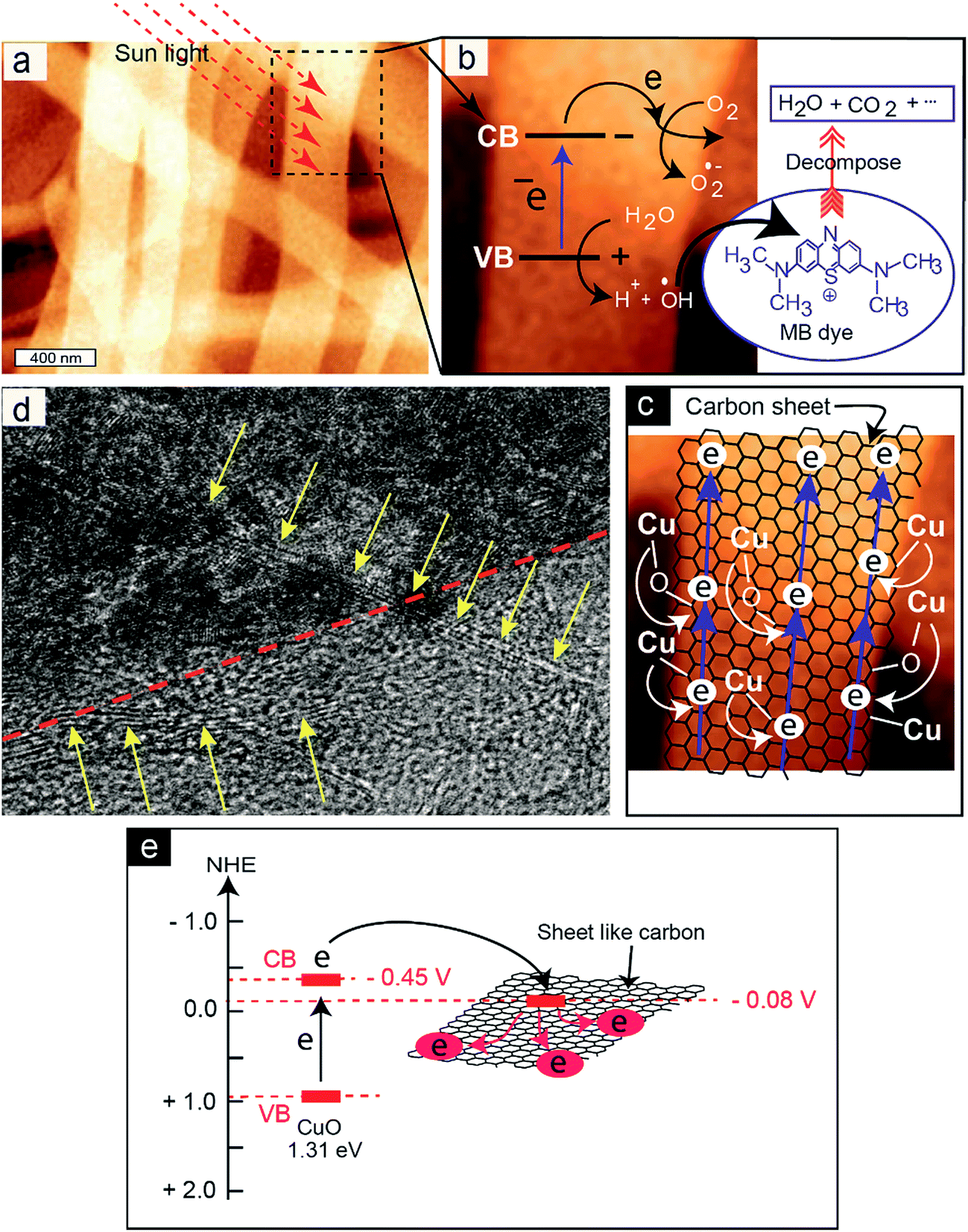
Fig. 7 shows a possible mechanism of the decomposition of MB with the help of a C-CuO nanoribbon photocatalyst. When a porous CuO nanoribbon is exposed to sunlight (Fig. 7a), an electron is excited from its valence band (VB) to its conduction band (CB) (Fig. 7b). This photoexcited electron in the conduction band is transferred quickly to the nearest highly conductive carbon surface, as discussed above (Fig. 7c), by a bridging chemical bond because CuO is a p-type semiconductor with its valence and conduction band edges at +1.25 V and +0.45 V vs. NHE48 (Fig. 7e). On the other hand, the conduction band of carbon materials is at 0.08 V vs. NHE45,49,50 (Fig. 7e). Thus, due to irradiation by sunlight, electrons are excited from the valence band to the conduction band of CuO nanoribbon and these excited electrons are easily transferred to a convenient band position of the carbon sheet (Fig. 7e). The photoexcited electrons are then used to prepare O2˙− species47,51,52 (Fig. 7b) in the presence of dissolved oxygen in H2O on the two-dimensional surface of carbon.47,51,52 The prepared active O2˙− species are used to prepare active OH˙ free radicals in the presence of H+ followed by reaction (6).47,51,52 Here, H+ is prepared by reaction (5). Then, OH˙ directly attacks the MB dye molecule (Fig. 7b) (reaction (8)) for degradation.47,51,52 During photoexcitation, active OH˙ free radicals are also prepared from a H2O molecule (reaction (7)) (Fig. 7b) by reaction with a hole in the VB.47,51,52 Here, the decomposition of MB is achieved by attacking the active OH˙ (Fig. 7b) in the VB. Recombination of the photoexcited electron from the CB to VB is unlikely due to the rapid transfer of electrons to the adjacent highly conductive carbon surface. The highly conductive carbon can quickly receive this photoexcited electron via its possible bridging chemical bond with CuO (i.e., Cu–C, Cu–O–C or Cu–O–O–C), as shown in Fig. 7c. Therefore, carbon acts as an inhibitor of recombination and increases the decomposition rate in a photocatalysis reaction, which is very important for the photocatalysis reaction. The presence of a carbon sheet is shown by the HRTEM image in Fig. 7d. The yellow arrows clearly indicate the edge of a carbon sheet with few layers. The edge of the C-CuO nanoribbon is shown by the red dotted line.
| |
 | (7) |
| |
 | (8) |
| |
 | (9) |
| |
 | (10) |
 |
| | Fig. 7 Photodegradation mechanism: (a) solar light is incident on the C-CuO nanoribbon, (b) electrons are excited from the VB to the CB and transferred via carbon to finally produce OH˙ species, which are used to decompose the dye, (c) electrons are transferred to the carbon sheet via a chemical bond, (d) HRTEM image of C-CuO nanoribbon in which the edge is shown by the red dotted line. The area above the red dotted line is CuO nanoparticles. The yellow arrow indicates the edge of a carbon sheet with few layers. (e) Band positions of CuO nanoribbon and carbon materials, showing a convenient band for transferring electron to the carbon sheet from the conduction band of CuO nanoribbon. | |
4. Conclusions
Porous C-CuO nanoribbons were prepared in solution using a novel facile route without a substrate. A substrate is a significant barrier for separating prepared C-CuO nanoribbons from the substrate surface for dispersion in a solution for other application purposes. This substrate-free process is performed without a catalyst, template or costly instrumentation at room temperature. Furthermore, the precursor materials and solvent used are of general grade having a low cost. The concentration of a dispersion (4.37 mg mL−1) of the C-CuO nanoribbon in ethanol solvent was also measured, which is a very high concentration and indicates very high dispersion stability. Because the prepared nanoribbon can be dispersed in other organic solvents, thus the prepared C-CuO can be used in other organic media for the deposition of other materials on it. Its light absorption capabilities (400–1665 nm) with high intensity, dye degradation performance of 96.6% (deducting self-degradation), utilization of direct sunlight as a light source and photostability against photocorrosion for up to 24 cycles indicate that the C-CuO nanoribbon is an excellent photocatalyst in an outdoor environment under direct sunlight. Considering its simplicity, reaction time, production cost, production yield, environmental friendliness, and photocatalytic performance, this process provides the best opportunity for the large-scale industrial production of C-CuO nanoribbon.
Acknowledgements
This study was supported by the Priority Research Centers Program through the National Research Foundation of Korea (NRF) funded by the Ministry of Education (2014R1A6A1031189).
References
- Y. Cui, Q. Q. Wei, H. K. Park and C. M. Lieber, Science, 2001, 293, 1289–1292 CrossRef CAS PubMed.
- F. Favier, F. C. Walter, M. P. Zach, T. Benter and R. M. Penner, Science, 2001, 293, 2227–2231 CrossRef CAS PubMed.
- M. H. Huang, S. Mao, H. Feick, H. Q. Yan, Y. Y. Wu, H. Kind, E. Weber, R. Russo and P. D. Yang, Science, 2001, 292, 1897–1899 CrossRef CAS PubMed.
- L. J. Lauhon, M. S. Gudiksen, D. L. Wang and C. M. Lieber, Nature, 2002, 420, 57–61 CrossRef CAS PubMed.
- F. Qian, G. Wang and Y. Li, Nano Lett., 2010, 10, 4686–4691 CrossRef CAS PubMed.
- Y. Feng and X. Zheng, Nano Lett., 2010, 10, 4762–4766 CrossRef CAS PubMed.
- Q. Yu, H. Huang, R. Chen, P. Wang, H. Yang, M. Gao, X. Peng and Z. Ye, Nanoscale, 2012, 4, 2613–2620 RSC.
- Z. Zhang, R. Dua, L. Zhang, H. Zhu, H. Zhang and P. Wang, ACS Nano, 2013, 7, 1709–1717 CrossRef CAS PubMed.
- A. Kargar, Y. Jing, S. J. Kim, C. T. Riley, X. Pan and D. Wang, ACS Nano, 2013, 7, 11112–11120 CrossRef CAS PubMed.
- H. Zhou and S. S. Wong, ACS Nano, 2008, 2, 944–958 CrossRef CAS PubMed.
- S. Yuan, X. Huang, D. Ma, H. Wang, F. Meng and X. Zhang, Adv. Mater., 2014, 26, 2273–2279 CrossRef CAS PubMed.
- S. Sahoo, S. Husale, B. Colwill, T. Lu, S. Nayak and P. M. Ajayan, ACS Nano, 2009, 3, 3935–3944 CrossRef CAS PubMed.
- X. Wen, W. Zhang, S. Yang, Z. R. Dai and Z. L. Wang, Nano Lett., 2002, 2, 1397–1401 CrossRef CAS.
- X. Jiang, T. Herricks and Y. Xia, Nano Lett., 2002, 2, 1333–1338 CrossRef CAS.
- Y. Qin, Y. Yang, R. Scholz, E. Pippel, X. Lu and M. Knez, Nano Lett., 2011, 11, 2503–2509 CrossRef CAS PubMed.
- Y. Feng, I. S. Cho, P. M. Rao, L. Cai and X. Zheng, Nano Lett., 2013, 13, 855–860 CrossRef CAS PubMed.
- Y. Zhou, S. Kamiya, H. Minamikawa and T. Shimizu, Adv. Mater., 2007, 19, 4194–4197 CrossRef CAS.
- B. Sciacca, S. A. Mann, F. D. Tichelaar, H. W. Zandbergen, M. A. V. Huis and E. C. Garnett, Nano Lett., 2014, 14, 5891–5898 CrossRef CAS PubMed.
- Z. Zhang, R. Dua, L. Zhang, H. Zhu, H. Zhang and P. Wang, ACS Nano, 2013, 7, 1709–1717 CrossRef CAS PubMed.
- W. Wang, G. Wang, X. Wang, Y. Zhan, Y. Liu and C. Zheng, Adv. Mater., 2002, 14, 67–69 CrossRef CAS.
- B. Liu and H. C. Zeng, J. Am. Chem. Soc., 2004, 126, 8124–8125 CrossRef CAS PubMed.
- R. Gusain and O. P. Khatri, J. Mater. Chem. A, 2013, 1, 5612–5619 CAS.
- K. Y. Lee, H. Hwang, D. Shin and W. Choi, J. Mater. Chem. A, 2015, 3, 5457–5466 CAS.
- S. Hsieh, P.-Y. Lin and L.-Ya. Chu, J. Phys. Chem. C, 2014, 118, 12500–12505 CAS.
- C.-C. Teng, C.-C. M. Ma, C.-H. Lu, S.-Y. Yang, S.-H. Lee, M.-C. Hsiao, M.-Y. Yen, K.-C. Chiou and T.-M. Lee, Carbon, 2011, 49, 5107–5116 CrossRef CAS.
- Y.-P. Zhu, M. Li, Y.-L. Liu, T.-Z. Ren and Z.-Y. Yuan, J. Phys. Chem. C, 2014, 118, 10963–10971 CAS.
- X. Zhou, Y. Li, T. Peng, W. Xie and X. Zhao, Mater. Lett., 2009, 63, 1747–1749 CrossRef CAS.
- Z.-J. Zuo, J. Li, P.-D. Han and W. Huang, J. Phys. Chem. C, 2014, 118, 20332–20345 CAS.
- L. Pan, J.-J. Zou, T. Zhang, S. Wang, Z. Li, L. Wang and X. Zhang, J. Phys. Chem. C, 2014, 118, 16335–16343 CAS.
- X. Qiu, M. Miyauchi, K. Sunada, M. Minoshima, M. Liu, Y. Lu, D. Li, Y. Shimodaira, Y. Hosogi, Y. Kuroda and K. Hashimoto, ACS Nano, 2012, 6, 1609–1618 CrossRef CAS PubMed.
- L. Zhang, D. A. Blom and H. Wang, Chem. Mater., 2011, 23, 4587–4598 CrossRef CAS.
- M. T. Qamar, M. Aslam, I. M. I. Ismail, N. Salah and A. Hameed, ACS Appl. Mater. Interfaces, 2015, 7, 8757–8769 CAS.
- H.-Y. Jiang, G. Liu, M. Li, J. Liu, W. Sun, J. Ye and J. Lin, Appl. Catal., B, 2015, 163, 267–276 CrossRef CAS.
- M. D. Susman, Y. Feldman, A. Vaskevich and I. Rubinstein, ACS Nano, 2014, 8, 162–174 CrossRef CAS PubMed.
- G. Yin, M. Nishikawa, Y. Nosaka, N. Srinivasan, D. Atarashi, E. Sakai and M. Miyauchi, ACS Nano, 2015, 9, 2111–2119 CrossRef CAS PubMed.
- H. Weidong, Q. Wei, W. Xiaohong and N. Hailong, Mater. Lett., 2007, 61, 4100–4102 CrossRef.
- M. Samadi, H. A. Shivaee, M. Zanetti, A. Pourjavadi and A. Moshfesgh, J. Mol. Catal. A: Chem., 2012, 359, 42–48 CrossRef CAS.
- M. M. Hossain, B.-C. Ku and J. R. Hahn, J. Appl. Surf. Sci., 2015, 354, 55–65 CrossRef CAS.
- B. L. Hurley and R. L. McCreery, J. Electrochem. Soc., 2004, 151, B252–B259 CrossRef CAS.
- D. I. Son, B. W. Kwon, D. H. Park, W. S. Seo, Y. Yi, B. Angadi, C. L. Lee and W. K. Choi, Nat. Nanotechnol., 2012, 7, 465–471 CrossRef CAS PubMed.
- L. Xu, G. Zheng, J. Wang, M. Lai, J. Miao, F. Xian, F. Gu and T. Sun, Mater. Lett., 2014, 122, 1–4 CrossRef CAS.
- Y. Yan, Z. Zhou, W. Li, Y. Zhu, Y. Cheng, F. Zhao and J. Zhou, RSC Adv., 2014, 4, 38558–38567 RSC.
- C. Han, M.-Q. Yang, B. Weng and Y.-J. Xu, Phys. Chem. Chem. Phys., 2014, 16, 16891–16903 RSC.
- Y. Zhang, Z.-R. Tang, X. Fu and Y.-J. Xu, ACS Nano, 2010, 4, 7303–7314 CrossRef CAS PubMed.
- C. Han, Z. Chen, N. Zhang, J. C. Colmenares and Y.-J. Xu, Adv. Funct. Mater., 2015, 25, 221–229 CrossRef CAS.
- M.-Q. Yang, N. Zhang, M. Pagliaro and Y.-J. Xu, Chem. Soc. Rev., 2014, 43, 8240–8254 RSC.
- N. Zhang, M.-Q. Yang, S. Liu, Y. Sun and Y.-J. Xu, Chem. Rev., 2015, 115, 10307–10377 CrossRef CAS PubMed.
- M. T. Qamar, M. Aslam, I. M. I. Ismail, N. Salah and A. Hameed, ACS Appl. Mater. Interfaces, 2015, 7, 8757–8769 CAS.
- M.-Q. Yang and Y.-J. Xu, Phys. Chem. Chem. Phys., 2013, 15, 19102–19118 RSC.
- J. Zhang, J. Yu, M. Jaroniec and J. R. Gong, Nano Lett., 2012, 12, 4584–4589 CrossRef CAS PubMed.
- A. Houas, H. Lachheb, M. Ksibi, E. Elaloui, C. Guillard and J.-M. Herrmann, Appl. Catal., B, 2001, 31, 145–157 CrossRef CAS.
- T. S. Natarajan, K. Natarajan, H. C. Bajaj and R. J. Tayade, J. Nanopart. Res., 2013, 15, 1669 CrossRef.
|
| This journal is © The Royal Society of Chemistry 2016 |
Click here to see how this site uses Cookies. View our privacy policy here.