
Direct synthesis of graphene quantum dots from multilayer graphene flakes through grinding assisted co-solvent ultrasonication for all-printed resistive switching arrays†
Junaid Alia,
Ghayas-ud-din Siddiquia,
Young Jin Yanga,
Kang Taek Leeb,
Kiju Umb and
Kyung Hyun Choi*a
aDepartment of Mechatronics Engineering, Jeju National University, 690-756, Korea. E-mail: amm@jejunu.ac.kr; Tel: +82 1098983713
bDepartment of Chemical and Biomolecular Engineering, Yonsei University, 120-749, Korea
First published on 7th January 2016
Abstract
Graphene quantum dots (GQD) with diameters as small as ∼2 nm were synthesized by an efficient chemo-mechanical technique. This involved mortar grinding and ultra-sonication as a means of mechanical energy transfer, while N-methyl-pyrrolidone and 1,2-dichlorobenzene were used for exfoliation and breakdown of graphene nanoplatelets. High resolution transmission electron microscopy images showed that the solution-based GQDs were about 2–4 nm in size, and had a crystalline lattice parameter of 0.24 nm. The technique proved useful for extracting GQDs of the desired size. XRD, Raman and FTIR spectroscopy were used to analyze the quality of the graphene structure within the GQDs. The UV responsive GQDs had a band-gap of 2.6 eV and stronger photoluminescence at 350 nm compared to lower wavelengths of laser excitation. An all-printed 2 × 2 array of memristors based on a GQD embedded polymer matrix fabricated on a flexible PET substrate showed an OFF/ON ratio of just over 7 when read at 100 mV, stable retention despite a high compliance current for ∼100 switching cycles, and a robustness of 200 bending cycles up to 1.5 cm bending diameter without compromise on resistive switching states.
1. Introduction
Graphene is a crystalline two-dimensional (2D) single carbon atom thick sheet of carbon atoms arranged in a hexagonal lattice.1 The simple yet effective work by Novoselov et al.1 on electric field effects in graphene films was the first report on a stable isolated planar graphene. It has been a revolutionary material due to its unique thermal,2 optoelectronic,3 magnetic,4 superconducting5 and semiconducting6 properties. It has no band-gap with an infinite Bohr radius that imparts metal-like conductivity to graphene sheets, thus showing the possibility of confinement for any finite size of graphene.7 Band-gap induced graphene in the form of graphene quantum dots (GQDs) and nanoribbons has attracted great interest in recent years. GQDs are zero dimensional sp2 hybridized carbon systems, the same as the three dimensional (3D) structure in the case of graphite, 2D graphene, or one-dimensional (1D) carbon nanotubes. Graphite is in fact multi-stacked graphene, whereas carbon nanotubes (CNTs) are graphene sheets rolled up into cylinders. GQDs are typically smaller than 20 nm in diameter8 comprised of single or multilayer graphene. GQDs have numerous proven applications in bio imaging9 and photonic devices such as solar cells,10 photodetectors,11 light emitting diodes12 and many others due to the altered quantum confinement and presence of edge states.13 GQDs are often synthesized by breaking materials comprised of 2D graphene sheets into 0D nanostructures. Compared with carbon dots, GQDs also have higher surface to volume ratio and the remarkable, graphene structure, hence providing them with comparatively superior properties.There are various methods for GQD synthesis that can be divided into two major approaches: top down and bottom up approaches. Top down approaches involve the breaking down of mesoscopic 1D, 2D or 3D graphene structures such as CNTs, graphite, graphene platelets or carbon fibers into smaller fragments by hydrothermal,14 solvo-thermal,15 electro-chemical,16 microwave assisted hydrothermal17 or nanolithography18 to smaller fragments. The hydrothermal route involves separate graphene oxide cleaving and reduction processes, which require up to three days.19 In bottom up approaches, such as hexaphenylbenzene pyrolysis,20 tetra-phenyl-cyclo-pentadienones and diphenyl ether reflux under argon atmosphere21 or laser exposure of benzene22 and compounds containing fullerenes like polycyclic aromatic molecules are used to synthesize GQDs. Most of these methods either use acids23,24 or high temperature treatments during synthesis.
It is highly desirable to improve the synthesis of GQD with a desired size by minimizing the need for expensive equipment, high temperature process, and highly caustic and hazardous chemicals. In this study, a direct ultra-sonication assisted GQD synthesis approach was developed, which involves grinding and ultra-sonication in the presence of two solvents without the use of any acidic reagents,23,24 high temperature treatments, or sophisticated apparatus.22,25 The approach presented here is scalable, offers a high yield of ∼7 mg ml−1 and low cost synthesis of GQDs of desired size. The study also describes the significance and compatibility of the approach for solution process technologies to integrate the as synthesized GQDs in printed electronic devices, without addition of new solvents that may harm quality of GQDs. Here the solution processable GQDs embedded polymer thin films have been printed using electrohydrodynamic atomization (EHDA)26 and employed in all printed flexible array of resistive switching devices. The successful integration of the approach with solution processable printing can assist future development of other GQDs based, thin film electronic and optoelectronic devices.
2. Experimental section
Synthesis of graphene quantum dots
Graphene flakes were purchased from Cheap Tubes (44 layers and surface area 750 m2 g−1), and N-methyl-pyrrolidone (NMP) and 1,2 dichlorobenzene (DCB) were purchased from Sigma Aldrich. All reagents were used as received without any further purification. First, 120 mg of graphene flakes and a few drops of NMP were poured in a mortar and then ground for 360 minutes using a pestle. The NMP was added to keep the powder moist to assist in grinding and exfoliation. The ground graphene was then dried at 100 °C for 1 h, and the powder was extracted and weighed for further processing. Next, 10 ml NMP, 10 ml DCB and 100 mg ground and dried powder were added in a cleaned bottle. The three were mixed thoroughly with a magnetic stirrer for 1 h at 1000 rpm at room temperature, followed by mechanical shaking for 4 h at 300 rpm. After mixing, the product was sonicated in an ice pack filled water bath for 4 h at room temperature. A Fisher Scientific Sonic Dismembrator (100 W) was used for ultra-sonication for 1 h to break the graphene sheets into even smaller fragments. The supernatant was collected after centrifugation for 30 min, using a WiseSpin (CF-10) at 5000, 8000, 10![[thin space (1/6-em)]](https://www.rsc.org/images/entities/char_2009.gif) 000 and 13500 rpm rotation speeds, named as samples S-1, S-2, S-3, and S-4, respectively. The supernatants were dried by evaporation of the solvents in air at 100 °C. Finally, the dried GQD powder was used for XRD and Raman characterizations.
000 and 13500 rpm rotation speeds, named as samples S-1, S-2, S-3, and S-4, respectively. The supernatants were dried by evaporation of the solvents in air at 100 °C. Finally, the dried GQD powder was used for XRD and Raman characterizations.
Synthesis of precursor for active layer fabrication
A small quantity of Poly(4-Vinyl Phenol) (PVP) in ratio 2:1 with GQDs was added to the GQD dispersion in NMP/DCB from sample S-3 to synthesize the solution processable PVP:GQD nanocomposite. For uniform dispersion of PVP:GQD, bath sonication was used for 10 min and ultrasonication for 5 min.
Fabrication of all-printed resistive switching device
For the fabrication of a flexible GQD–polymer nanocomposite memory device, mass printing technologies, such as EHDA and roll to plate were employed. A 2 × 2 array of 4 resistive switching devices was fabricated with insulating polymer (PVP) used as host material for the GQDs. The top and cross section views of the device has been schematically shown in Fig. 1(a). PET substrates were cleaned using ethyl alcohol, deionized water and the exposed to UV light for 5 minutes. The development of the patterned Ag top and bottom electrodes was carried out similar to our previous work27 employing roll to plate technology. Here 11 kg F force waste applied for pattern transfer with a delay time of 3 s. Fine ∼250 μm wide Ag patterns were achieved after sintering the samples at 100 °C for 1 h as shown by optical microscope micrograph in Fig. 1(b). Prior to deposition of active layer, part of Ag bottom electrodes as columns was carefully masked by tape for electrical connections. The thin film of nanocomposite as active material (∼100 nm) was deposited using EHDA setup used in our previous work.28 After curing the deposited thin films at 100 °C for 2 h, rows of top electrodes were deposited on top of active layer again by roll to plate technology. The top and bottom electrodes crossed each other at 4 locations with active layer sandwiched between them, hence forming memristors Mem1–Mem4 shown by circles in Fig. 1(a).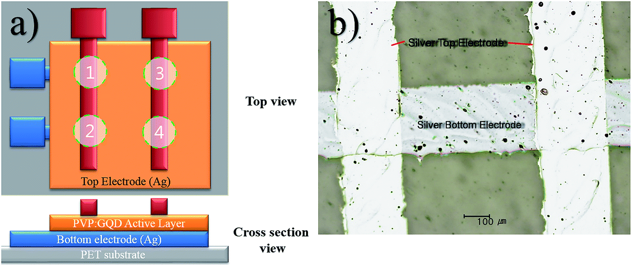 | ||
| Fig. 1 (a) Schematic diagram all printed GQD based flexible resistive switching 2 × 2 array top view [top left] and cross section view [bottom left]. (b) The optical microscope image showing the cross points of Ag electrodes sandwiching the solution processed transparent GQD embedded polymer active layer. | ||
Characterization
The synthesized GQDs were characterized by various techniques. TEM, HRTEM and SAED measurements were performed using a (JEM-ARM 200F) Cs-corrected STEM (spherical aberration correction scanning transmission electron microscope) operated at 200 kV. A Rigaku X-ray diffractometer was used for X-ray diffraction (XRD), operated at 36 kV and 36 mA (Cu Kα radiation λ = 1.541 Å) with a step of 0.02°. All UV-vis absorption spectra were obtained on a UV/VIS/NIR spectrophotometer (Lambda 25, Perkin Elmer). Raman scattering spectra were obtained at room temperature with a Horiba Jobin Yvon HR spectrometer using 514 nm excitation laser wavelength. Photoluminescence spectra were recorded by Perkin Elmer LS 55 Fluorescence spectrometer. Fourier transform infra-red spectroscopy (FT-IR) spectra of the samples were recorded on a Bruker IFS 66 V spectrometer using the KBr pellet method with a resolution of 4 cm−1 in the range of 4000 to 100 cm−1. Agilent B1500A Semiconductor Device Analyzer was used for analyzing the resistive switching characteristics of the as-fabricated devices by current–voltage (I–V) measurements. The surface morphology of thin GQD embedded polymer film was studied using JSM-6700F field-emission scanning electron microscope (FESEM). Film thickness was measured by a non-destructive, thin film-thickness machine, K-MAC ST4000-DLX, based on interference spectrum of white light incident on the film surface.3. Results and discussion
The GQDs were prepared by a sonication-assisted mechanical method. This approach involved first grinding few layer graphene flakes (GF) for 360 min in presence of N-methy l-2-pyrrolidone (NMP) to assist the exfoliation process, as well as to break down the flakes to smaller sizes.29 Afterwards, violent shaking and ultra-sonication in the presence of 1,2 dichlorobenzene (DCB), in addition to NMP, helped further break down the graphene to even smaller fragments.30,31 DCB has already been reported as a good organic solvent for exfoliation of graphene.32 Fig. 2 shows the flow diagram of the proposed chemo-mechanical process. The last stage of the process was centrifugation at high rotational speeds. Only supernatant species were collected for further characterization, since the sediments were expected to have a wide range of graphene sizes.33 The processed GF, collected before and after centrifugation have been shown in Fig. 2. The color change from opaque black to transparent golden yellow is clearly depicted in the photographs of the GQD sample before and after centrifugation. The flakes were broken down into smaller fragments during the chemo-mechanical treatment. The presence of NMP helped exfoliate the graphene, whereas the DCB was helpful for unzipping and the extraction of the GQDs.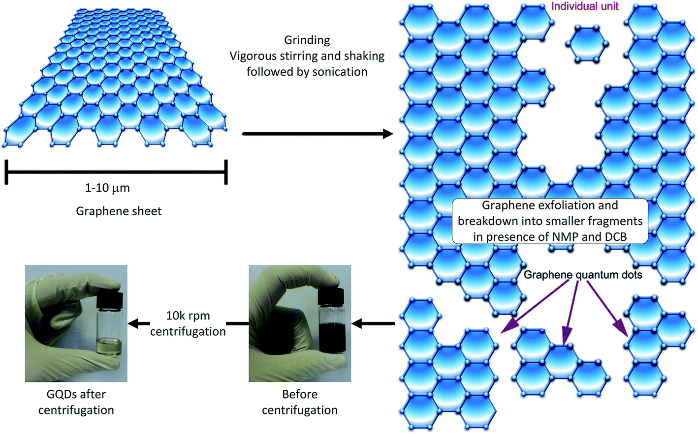 | ||
| Fig. 2 Schematic of graphene QD synthesis by the co-solvent, grinding and ultra-sonication-assisted mechanical route. The graphene sheets were broken down initially by grinding, and then through ultra-sonication in the presence of NMP and DCB. The supernatant species extracted as a result of centrifugation showed a transparent golden yellow color compared to the opaque char black for chemo-mechanically processed graphene before centrifugation. | ||
Transmission electron microscopy (TEM) investigation of unprocessed graphene flake in Fig. 3(a) shows few to single layer graphene sheet with long range crystalline order. Whereas the selected area electron diffraction pattern in Fig. 3(b) shows the characteristic crystalline graphene.34,35 The surface scan histogram in Fig. 3(c) obtained by evaluation of the high resolution TEM analysis of GF shows lattice parameter of 0.24 nm in agreement with literature.36
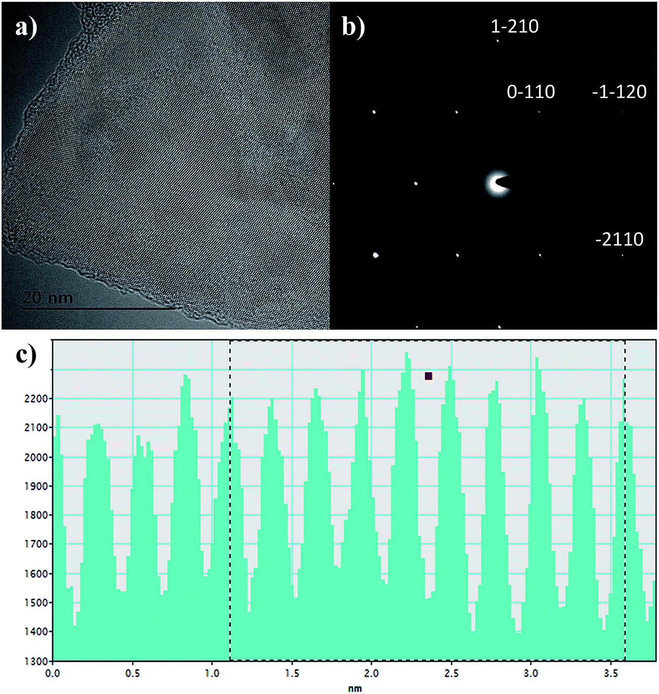 | ||
| Fig. 3 (a) HRTEM analysis of graphene flake in the sediment after processing shows crystallinity. (b) The SAED pattern shows six-fold symmetry for graphene crystal structure, and (c) the 2D surface scan profile shows the characteristic lattice spacing of about 0.24 nm. | ||
TEM investigation was carried out for samples, S-1, S-2, S-3, and S-4, obtained after final centrifugation at 5000, 8000, 10000 and 13500 rpm respectively for 30 min as shown in Fig. 4(a). Nano-Measurer 1.2 was used for calculating the diameters by analyzing the TEM images of each sample. The insets show the high resolution TEM of individual GQDs from each of the four samples with lattice spacing of 0.24 nm and highly crystalline structure. 2D FFT pattern (shown in inset) of the TEM image of one of the GQD samples also validated the presence of the characteristic hexagonal graphene structure.37 The average diameters of the GQDs collected after various centrifugation speeds have been tabulated in Table S1.†
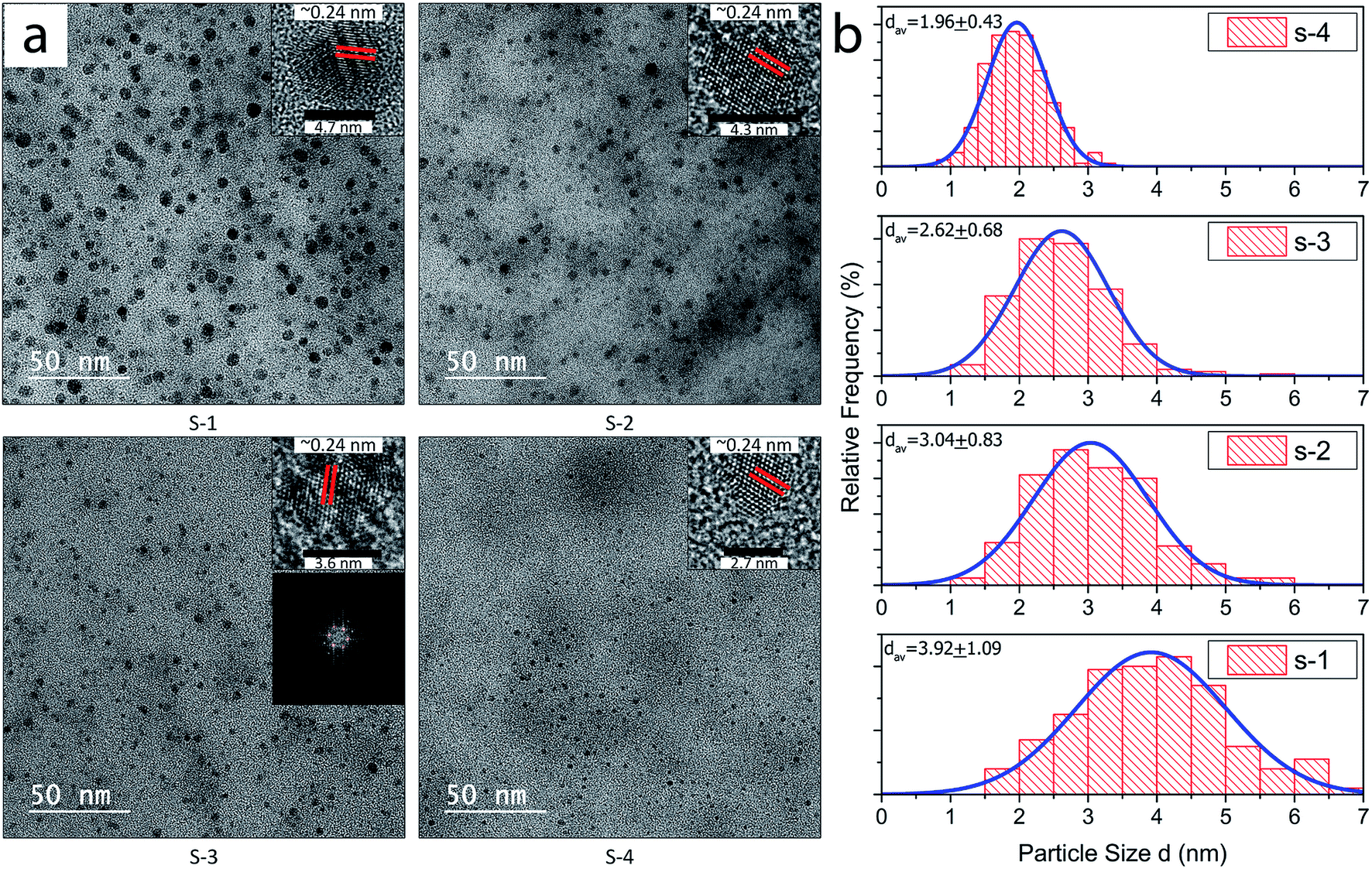 | ||
| Fig. 4 (a) TEM images of GQDs extracted at different centrifugation speeds: S-1 at 5000, S-2 at 8000, S-3 at 10000 and S-4 at 13500 rpm. The insets show respective HRTEM images of the GQDs from each sample, showing 0.24 nm lattice spacing. The 2D FFT of the GQD TEM image also showed the six fold rotation symmetry for the graphene lattice, and also provides evidence of crystallinity. (b) The diameter distribution of the extracted GQDs samples S-1 through S-4. Diameter distribution in each sample agrees with Gaussian distribution. The average QD size in each GQD sample decreases appreciably, from about 4 nm @ 5000 rpm to about 2 nm @ 13500 rpm centrifugation, performed for the 30 min for each sample. | ||
The size distribution of the extracted GQDs obtained by variation of centrifugation speed has been plotted in Fig. 4(b). Diameters of 200 GQDs spotted from TEM images were calculated for each sample. The average size of GQD in S-1 was 3.92 ± 1.09 nm, the largest among the 4 samples. The average GQD diameters for S-2 and S-3 were 3.04 ± 0.83 nm and 2.62 ± 0.68 nm, respectively. Sample S-4 had the smallest GQDs among the four, with an average size of 1.96 ± 0.43 nm, and also showed the narrowest distribution compared to the samples centrifuged at lower speeds. All samples accorded well with Gaussian distribution. The change in diameters of the extracted GQDs showed an inverse relation with the centrifugation speed, as shown in Fig. 5. Thus, it was inferred that it is possible to extract GQDs of the desired size from the supernatant by controlling the centrifugation speed.38
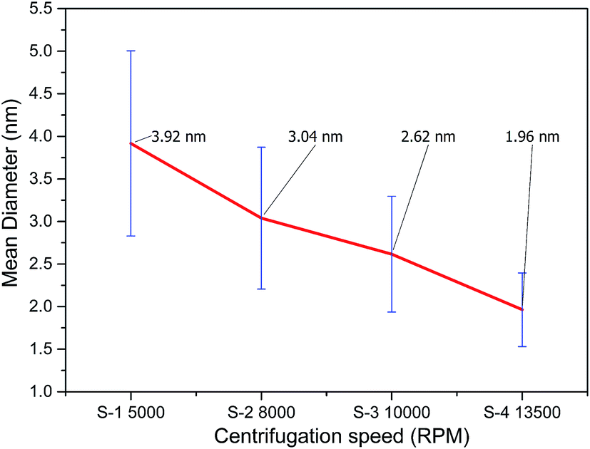 | ||
| Fig. 5 The change in GQD diameter with centrifugation speed is plotted, showing a decrease in average size and increase in homogeneity of the GQDs extracted at high centrifugation speeds. The average GQD size was least in the case of the fastest centrifugation of 13500 rpm. | ||
The chemical analysis for presence of graphene phase in sample was Raman, XRD, XPS and FTIR analyses. The solvents from sample S-3 were evaporated and GQD powder was collected for XRD and Raman spectral analyses, to confirm the quality of as-prepared GQDs. The Raman spectra shown in Fig. 6(a) reveal the existence of the D band at 1353 cm−1 corresponding to the disorder-induced phonon mode in GQD sample. This band involves iTO phonon around the K-point like the 2D band.39 The G band at 1591 cm−1 corresponding to Raman-allowed E2g phonon mode of vibrations was observed due to existence of graphitic structures.22,40 The ratio of peak intensities for the D and G bands ID/IG of graphene-containing species determines the graphene crystallinity. The ID/IG determined from the Raman peaks was about 0.88, Raman spectroscopy confirms the quality of the as-prepared GQD in powder sample.41,42 A typical X-ray diffraction (XRD) profile for synthesized GQD is shown in Fig. 6(b). The 2θ diffraction peak at 25° corresponded to the 002 peak of graphitic structure. The diffraction peak was in the range of 21° to 29°. The size and orientation of the GQDs in the powder sample increased the peak width. The d spacing for the GQDs powder was calculated to be 3.4 Å, using the relation dsinθ = nλ, was in good agreement with the reported values (3.40–4.81).24 Here, in the formula ‘n’ is the diffraction order taken as 1 for first order diffraction, and λ = 1.54 nm for Cu Kα line. Fig. 6(c) summarizes the Fourier transform infrared (FTIR) spectroscopy of the GQDs in sample S-3, DCB and NMP, respectively to explore the bonding composition. DCB showed absorption peaks at 578 cm−1 for C–Cl stretching, 1066 cm−1 for C–O–C stretching, and 1358 cm−1 for C–H rocking due to alkanes. The IR spectrum of NMP showed the characteristic strong carbonyl peak at 1742 cm−1, which was absent in the GQD samples. Comparison with the FTIR spectrum of GQD showed almost complete evaporation of the solvents during powder extraction. An obvious absorption peak centered at 1674 cm−1 (ref. 8) was caused by C![[double bond, length as m-dash]](https://www.rsc.org/images/entities/char_e001.gif) C stretching of aromatic rings.22 The broad peak centered at 3429 cm−1 indicates the presence of hydroxyl species in the sample, which might assist with the solubility of GQDs in water.43 The peaks at 1380 cm−1 and 2924 cm−1 showed the presence of C–H on the surface of the GQDs,22 presumably originating from alkyl groups. The 1262 cm−1 peak was attributed to the presence of C–O–C. The XPS studies were carried out to assess the concentration of oxygen in GQDs for sample S-3. The Carbon content atomic percentage was 94.9% compared to 5.1% oxygen as seen by the C1s and O1s peaks in XPS spectrum in Fig. 6(d).
C stretching of aromatic rings.22 The broad peak centered at 3429 cm−1 indicates the presence of hydroxyl species in the sample, which might assist with the solubility of GQDs in water.43 The peaks at 1380 cm−1 and 2924 cm−1 showed the presence of C–H on the surface of the GQDs,22 presumably originating from alkyl groups. The 1262 cm−1 peak was attributed to the presence of C–O–C. The XPS studies were carried out to assess the concentration of oxygen in GQDs for sample S-3. The Carbon content atomic percentage was 94.9% compared to 5.1% oxygen as seen by the C1s and O1s peaks in XPS spectrum in Fig. 6(d).
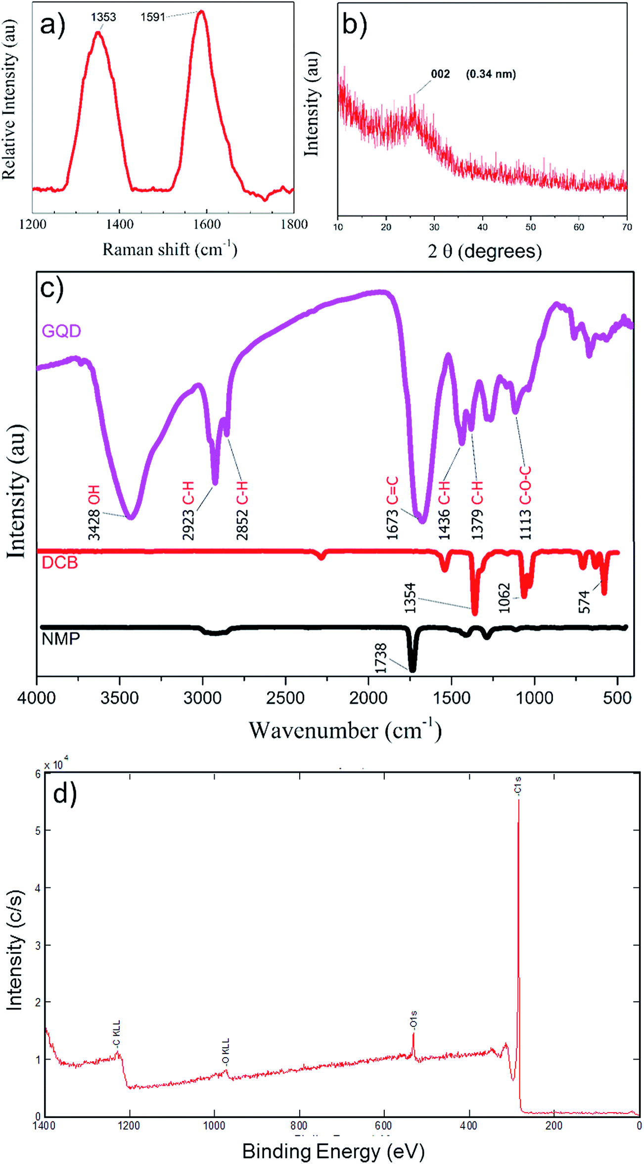 | ||
| Fig. 6 (a) The Raman spectrum of GQD powder extracted after evaporating the solvents from the GQDs of sample S-3 at 100 °C. The ratio of the intensities of the D band at 1321 cm−1 and the G band at 1590 cm−1 was about 0.73, which provides evidence of crystallinity within the GQD graphene phases. (b) The XRD profile of GQD powder extracted after drying out the NMP and DCB shows a wide 002 peak at around 25°. (c) Comparison of the FTIR of NMP, DCB and GQD powder sample shows complete evaporation of the solvents. The absence of a strong peak at 1742 cm−1 from NMP and at 1358 cm−1 from DCB when compared with the FTIR spectrum of GQD powder suggests the removal of both solvents inform the powder sample. (d) XPS analysis of GQD reveals high carbon content compared to other species. | ||
The UV visible absorption spectroscopy performed on the GQDs revealed weak shoulders at 322 nm and 364 nm,44 as shown in Fig. 7(a). The GQDs show a broad UV-vis absorption band with a strong shoulder at 289 nm (ref. 45) corresponding to n → π* transition due to CO, whereas a hump at 363 nm. These results are comparable to those obtained for samples prepared by the hydrothermal approach.19 UV absorption spectra were very difficult to compensate for strong absorption of NMP for wavelengths <265 nm. Therefore the UV absorption wavelengths below 265 nm are not discussed here. The bandgap for GQDs evaluated by Tauc plot as shown in Fig. 7(b) was about 2.6 eV, which shows promise for application of the GQDs in optoelectronics. The photoluminescence (PL) spectrum was obtained by exciting the GQD sample by a series of excitation wavelengths (λex) from 300 to 350 nm as shown in Fig. 7(c). The PL response for less than 300 nm excitation wavelengths is very low compared to that for 350 nm > λex > 300 nm. The PL emission was recorded in form of twin peaks at 442 nm (blue), and 493 nm (cyan) which steadily increased in PL intensity with λex without shift. For most values of λex, the intensity of 442 nm peak is less than that of 493 nm PL emission peak except for 310–330 nm excitation wavelengths. The GQDs excited at 350 nm showed most intense photoluminescence. All as-prepared GQD samples were pale yellow under ambient light and showed blue luminescence when illuminated by a 365 nm UV as photographed by hand phone camera in Fig. 7(d).
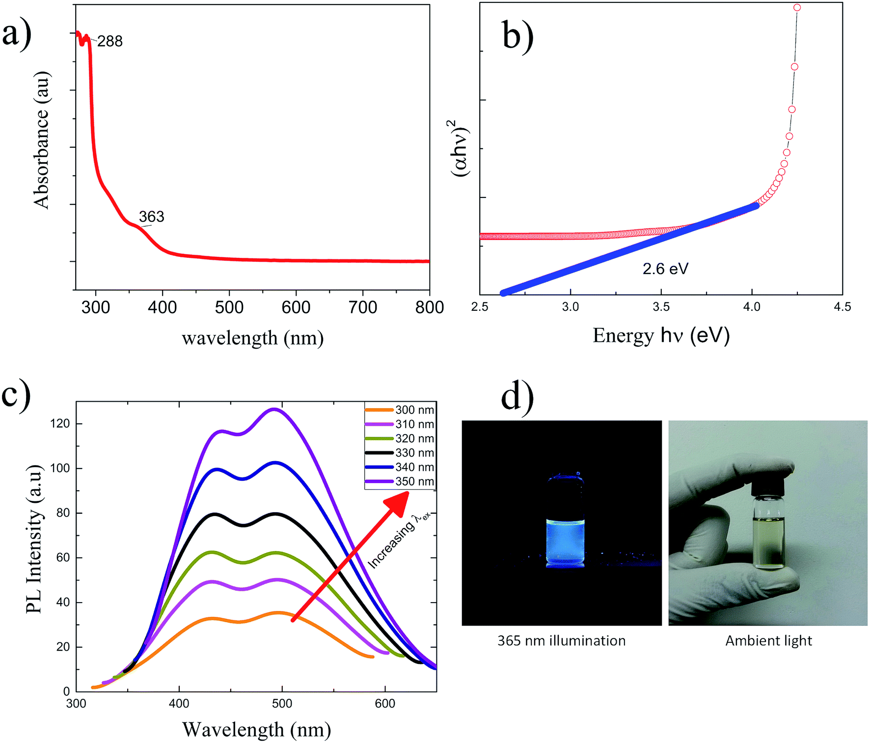 | ||
| Fig. 7 (a) The UV absorbance spectrum of GQD sample showed strong absorption in the UV region of the electromagnetic spectrum. The absorption subsided in the visible spectrum. (b) The energy bandgap calculated by Tauc plot for GQD showed x intercept at 2.6 eV. (c) PL properties of the GQDs. The PL spectrum shows twin peaks with strongest emission at 350 nm excitation wavelength compared to 300 nm through 350 nm. (d) The GQDs in golden yellow ambient light show blue luminescence for a 365 nm UV lamp illumination. | ||
4. All-printed resistive switching device
The GQDs from sample S-3 centrifuged at 10k rpm, were used for resistive switching device fabrication. Fig. 8(a) and (b) show respective high and low resolution FESEM images of nanocomposite thin films evidently prove the uniformity of the thin film. The thickness measurement was averaged after taking at least seven readings at different locations in such a way that the measurement represents almost all the area of thin film surface. The calculated thickness was 120 ± 19 nm. In order to study the electrical properties of the as-fabricated 2 × 2 array of 4 resistive switching devices, current–voltage (I–V) measurements were performed at room temperature by using a semiconductor characterization system.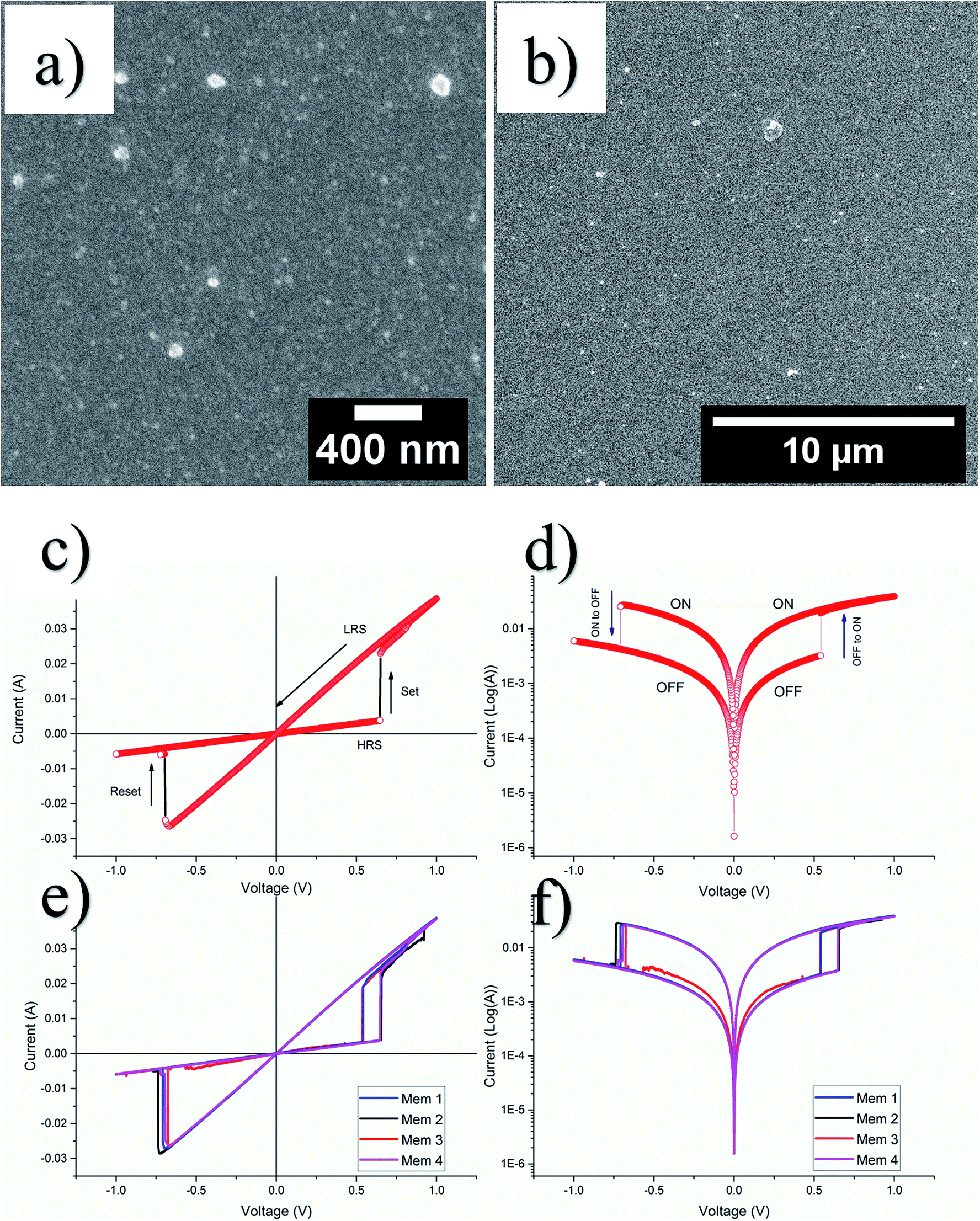 | ||
| Fig. 8 (a) High resolution (b) low resolution FESEM images. (c) First I–V and (d) semilog I–V plots for a memristor. (e) The comparison I–V and (f) semilog characteristics of four memristors of the 2 × 2 memristor array. | ||
For each of the as-fabricated Ag/PVP: GQD/Ag memristor, the bottom Ag electrode was grounded whereas the bias was applied to the top Ag electrode. The voltage stress was applied on the highly resistive pristine device (>103 Ω), in a sequence of 0 V to +1 V to 0 V. By steady increase of the voltages imposed on individual device, a pronounced change of resistance from the pristine high resistance state (HRS) to the relative low resistance state (LRS) is observed at a SET voltage of about 0.65 V. After the transition from HRS (∼170 Ω) to LRS (∼28 Ω) the device remained in LRS, for the subsequent sweep from +1 V to 0 V. The device shows no current when voltage drops to 0 V. During steady voltage transition 0 V to −1 V to 0 V, the devices keep steady LRS state. The resistance steadily increases with increase in magnitude of negative voltage until it reaches RESET voltage, Vmax = −0.69 V. Beyond Vmax, the current decreases rapidly, switching device OFF to the HRS from LRS state as shown in Fig. 8(c). Fig. 8(d) elaborates the semilog I–V response of the same memristor. Fig. 8(e) and (f) compare the I–V and semilog I–V responses for each of the four devices. The four devices show negligible change in memristor parameters. The robustness of the array was tested by applying voltage stress cycles on each of the four devices. The voltage stress applied on the devices showed stable switching for 100 repeated voltage stresses shown in Fig. 9(a). The state retentivity analysis was undertaken by measuring the resistance states after suitable time intervals for more than 24 h as shown in Fig. 9(b). The striking difference for the GQD embedded PVP based memristor with other PVP based memristors fabricated in past was the ability to withstand higher currents without breakdown, despite operating at more than 50 mA compliance currents. The very small variation in resistance states for memristor M1 dictates stability of the device over large number of voltage cycles as well as time and showed stability for over well 24 h. To evaluate flexibility of the PET based memristor array, it was flexed for over 200 times, yet the device remained undeterred for its memristor function as shown in Fig. 9(c) whereas the devices had remarkable performance for repeated bending cycles. The minimum bending diameter of 1.5 cm was observed as stable limit for device to function without breakdown. The device broke down when bent for diameter 1.2 cm as shown in Fig. 9(d).
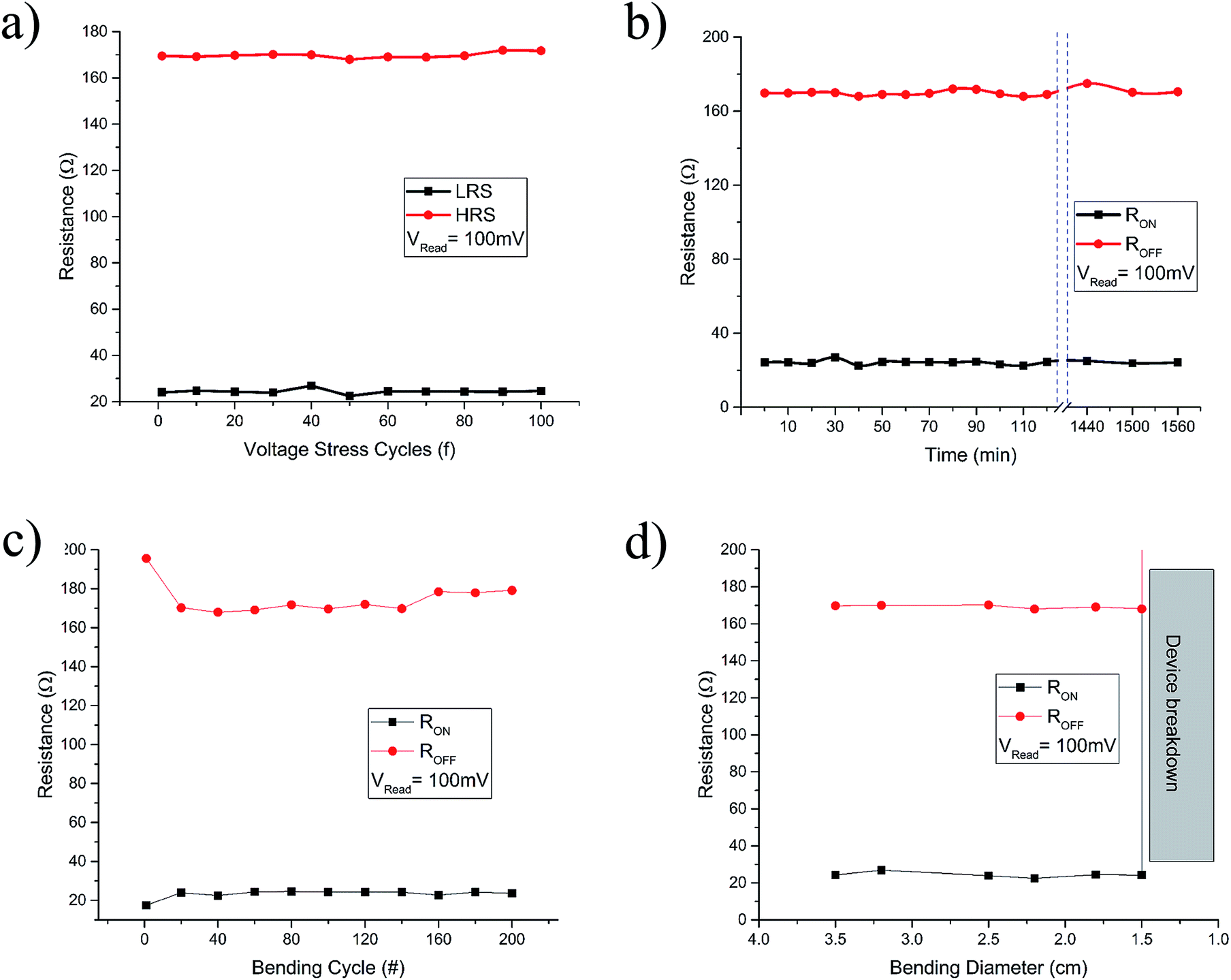 | ||
| Fig. 9 The resistive switching characteristics of the devices. (a) The voltage stress cycles (b), (c) retentivity and (d) flexibility tests performed for the memristors at Vread = 100 mV. | ||
5. Summary
GQDs were prepared directly from multilayer graphene flakes by grinding and ultra-sonication in the presence of two solvents, without the need for any acidic reagents. The approach is scalable, yet involves no sophisticated apparatus for the synthesis. In addition, it is also less time consuming. The yield of GQDs by the technique presented here is 7 mg ml−1, which is at par when compared to other similar techniques. The diameters of the GQDs extracted in a sample can also be controlled by the centrifugation speed. The GQDs showed strong absorption in UV and the deep UV region near 290 nm. The PL emission peaks were observed at 442 and 493 nm for laser excitation wavelengths from 300 to 350 nm. The peaks intensified with increase in λex. The GQD samples also showed blue luminescence in the presence of 365 nm UV source. Although this work was done entirely by hand milling in mortar by hand, it can be replaced by ball milling. This method provides an alternate to the existing hydrothermal techniques for GQD synthesis. The collected GQD have shown significance and solution processability for printed electronics, without compromising quality of GQDs during printing. EHDA printed PVP:GQDs active layer was sandwiched between roll to plate printed Ag patterns, in form of all printed flexible 2 × 2 array of resistive switching devices. GQD embedded polymer matrix based memristors showed OFF to ON ratio of about 10, robustness to withstand current in milliamps for more than 100 switching cycles, retentivity of resistance states intact for over 24 h. The array was also robust enough for more than 200 bending cycles without compromise on device functionality. The devices also showed bending ability for up to 1.5 cm. The successful integration of the approach with solution processable printing can assist future development of other GQDs based, thin film electronic and optoelectronic devices.
Conflict of interest
The authors declare no competing financial interests.Acknowledgements
This work was supported by a grant from the National Research Foundation of Korea (NRF), funded by the Korean government (MSIP) (No. NRF-2014R1A2A1A01007699).References
- K. S. Novoselov, A. K. Geim, S. V. Morozov, D. Jiang, Y. Zhang, S. V. Dubonos, I. V. Grigorieva and A. A. Firsov, Science, 2004, 306, 666–669 CrossRef CAS.
- A. A. Balandin, Nat. Mater., 2011, 10, 569–581 CrossRef CAS.
- F. Bonaccorso, Z. Sun, T. Hasan and A. C. Ferrari, Nat. Photonics, 2010, 4, 611–622 CrossRef CAS.
- O. V. Yazyev, Phys. Rev. Lett., 2008, 101, 037203 CrossRef PubMed.
- S.-L. Yang, J. A. Sobota, C. A. Howard, C. J. Pickard, M. Hashimoto, D. H. Lu, S.-K. Mo, P. S. Kirchmann and Z.-X. Shen, Nat. Commun., 2014, 5, 3493 Search PubMed.
- E. Castro, K. Novoselov, S. Morozov, N. Peres, J. Dos Santos, J. Nilsson, F. Guinea, A. Geim and A. Neto, Phys. Rev. Lett., 2007, 99, 216802 CrossRef.
- C. O. Kim, S. W. Hwang, S. Kim, D. H. Shin, S. S. Kang, J. M. Kim, C. W. Jang, J. H. Kim, K. W. Lee, S.-H. Choi and E. Hwang, Sci. Rep., 2014, 4, 5603 CAS.
- L. Tang, R. Ji, X. Cao, J. Lin, H. Jiang, X. Li, K. S. Teng, C. M. Luk, S. Zeng, J. Hao and S. P. Lau, ACS Nano, 2012, 6, 5102–5110 CrossRef CAS PubMed.
- B.-H. Jun, D. W. Hwang, H. S. Jung, J. Jang, H. Kim, H. Kang, T. Kang, S. Kyeong, H. Lee, D. H. Jeong, K. W. Kang, H. Youn, D. S. Lee and Y.-S. Lee, Adv. Funct. Mater., 2012, 22, 1843–1849 CrossRef CAS.
- Z. Liu, S. P. Lau and F. Yan, Chem. Soc. Rev., 2015, 44, 5638–5679 RSC.
- Q. Zhang, J. Jie, S. Diao, Z. Shao, Q. Zhang, L. Wang, W. Deng, W. Hu, H. Xia, X. Yuan and S.-T. Lee, ACS Nano, 2015, 9, 1561–1570 CrossRef CAS PubMed.
- M. Zubair, M. Mustafa, K. Lee, C. Yoon, Y. H. Doh and K. H. Choi, Chem. Eng. J., 2014, 253, 325–331 CrossRef CAS.
- K. A. Ritter and J. W. Lyding, Nat. Mater., 2009, 8, 235–242 CrossRef CAS PubMed.
- F. Yang, M. Zhao, B. Zheng, D. Xiao, L. Wu and Y. Guo, J. Mater. Chem., 2012, 22, 25471 RSC.
- L. Feng, X.-Y. Tang, Y.-X. Zhong, Y.-W. Liu, X.-H. Song, S.-L. Deng, S.-Y. Xie, J.-W. Yan and L.-S. Zheng, Nanoscale, 2014, 6, 12635–12643 RSC.
- D. B. Shinde and V. K. Pillai, Chem.–Eur. J., 2012, 18, 12522–12528 CrossRef CAS PubMed.
- L.-L. Li, J. Ji, R. Fei, C.-Z. Wang, Q. Lu, J.-R. Zhang, L.-P. Jiang and J.-J. Zhu, Adv. Funct. Mater., 2012, 22, 2971–2979 CrossRef CAS.
- L. A. Ponomarenko, F. Schedin, M. I. Katsnelson, R. Yang, E. W. Hill, K. S. Novoselov and A. K. Geim, Science, 2008, 320, 356–358 CrossRef CAS PubMed.
- D. Pan, J. Zhang, Z. Li and M. Wu, Adv. Mater., 2010, 22, 734–738 CrossRef CAS PubMed.
- R. Liu, D. Wu, X. Feng and K. Müllen, J. Am. Chem. Soc., 2011, 133, 15221–15223 CrossRef CAS PubMed.
- X. Yan, X. Cui and L.-S. S. Li, J. Am. Chem. Soc., 2010, 132, 5944–5945 CrossRef CAS PubMed.
- K. Habiba, V. I. Makarov, J. Avalos, M. J. F. Guinel, B. R. Weiner and G. Morell, Carbon, 2013, 64, 341–350 CrossRef CAS.
- R. Ye, C. Xiang, J. Lin, Z. Peng, K. Huang, Z. Yan, N. P. Cook, E. L. G. Samuel, C.-C. Hwang, G. Ruan, G. Ceriotti, A.-R. O. Raji, A. A. Martí and J. M. Tour, Nat. Commun., 2013, 4, 2943 Search PubMed.
- Z. Huang, Y. Shen, Y. Li, W. Zheng, Y. Xue, C. Qin, B. Zhang, J. Hao and W. Feng, Nanoscale, 2014, 6, 13043–13052 RSC.
- J. Lu, P. S. E. Yeo, C. K. Gan, P. Wu and K. P. Loh, Nat. Nanotechnol., 2011, 6, 247–252 CrossRef CAS PubMed.
- K. H. H. Choi, J. Ali and K.-H. Na, Phys. B, 2015, 475, 148–155 CrossRef CAS.
- K. Ali, J. Ali, S. M. Mehdi, K.-H. Choi and Y. J. Yang, Appl. Surf. Sci., 2015, 353, 1186–1194 CrossRef CAS.
- K. H. Choi, A. Ali, H. C. Kim and M. T. Hyun, J. Korean Phys. Soc., 2013, 62, 269–274 CrossRef CAS.
- J.-Y. Wu, M.-N. Lin, L.-D. Wang and T. Zhang, J. Nanomater., 2014, 2014, 1–7 Search PubMed.
- K. R. Paton, E. Varrla, C. Backes, R. J. Smith, U. Khan, A. O'Neill, C. Boland, M. Lotya, O. M. Istrate, P. King, T. Higgins, S. Barwich, P. May, P. Puczkarski, I. Ahmed, M. Moebius, H. Pettersson, E. Long, J. Coelho, S. E. O'Brien, E. K. McGuire, B. M. Sanchez, G. S. Duesberg, N. McEvoy, T. J. Pennycook, C. Downing, A. Crossley, V. Nicolosi and J. N. Coleman, Nat. Mater., 2014, 13, 624–630 CrossRef CAS PubMed.
- L. Kou, F. Li, W. Chen and T. Guo, Org. Electron., 2013, 14, 1447–1451 CrossRef CAS.
- T. Skaltsas, N. Karousis, H.-J. Yan, C.-R. Wang, S. Pispas and N. Tagmatarchis, J. Mater. Chem., 2012, 22, 21507 RSC.
- R. Jan, P. May, A. P. Bell, A. Habib, U. Khan and J. N. Coleman, Nanoscale, 2014, 6, 4889–4895 RSC.
- S. Stankovich, D. A. Dikin, G. H. B. Dommett, K. M. Kohlhaas, E. J. Zimney, E. A. Stach, R. D. Piner, S. T. Nguyen and R. S. Ruoff, Nature, 2006, 442, 282–286 CrossRef CAS PubMed.
- S. Kumar, E. Rezvani, V. Nicolosi and G. S. Duesberg, Nanotechnology, 2012, 23, 145302 CrossRef CAS PubMed.
- C. Zhu, S. Yang, G. Wang, R. Mo, P. He, J. Sun, Z. Di, N. Yuan, J. Ding, G. Ding and X. Xie, J. Mater. Chem. C, 2015, 3, 8810–8816 RSC.
- L. Lin and S. Zhang, Chem. Commun., 2012, 48, 10177–10179 RSC.
- U. Khan, A. O'Neill, M. Lotya, S. De and J. N. Coleman, Small, 2010, 6, 864–871 CrossRef CAS PubMed.
- R. Beams, L. Gustavo Cançado and L. Novotny, J. Phys.: Condens. Matter, 2015, 27, 083002 CrossRef PubMed.
- L. G. Cançado, A. Jorio, E. H. M. Ferreira, F. Stavale, C. A. Achete, R. B. Capaz, M. V. O. Moutinho, A. Lombardo, T. S. Kulmala and A. C. Ferrari, Nano Lett., 2011, 11, 3190–3196 CrossRef PubMed.
- S. Kim, D. Hee Shin, C. Oh Kim, S. Seok Kang, S. Sin Joo, S.-H. H. Choi, S. Won Hwang and C. Sone, Appl. Phys. Lett., 2013, 102, 2012–2015 Search PubMed.
- Y. Su, X. Lu, M. Xie, H. Geng, H. Wei, Z. Yang and Y. Zhang, Nanoscale, 2013, 5, 8889–8893 RSC.
- J. Peng, W. Gao, B. K. Gupta, Z. Liu, R. Romero-Aburto, L. Ge, L. Song, L. B. Alemany, X. Zhan, G. Gao, S. A. Vithayathil, B. A. Kaipparettu, A. A. Marti, T. Hayashi, J. Zhu and P. M. Ajayan, Nano Lett., 2012, 12, 844–849 CrossRef CAS PubMed.
- Y. Dong, J. Shao, C. Chen, H. Li, R. Wang, Y. Chi, X. Lin and G. Chen, Carbon, 2012, 50, 4738–4743 CrossRef CAS.
- L. Zhang, Z.-Y. Zhang, R.-P. Liang, Y.-H. Li and J.-D. Qiu, Anal. Chem., 2014, 86, 4423–4430 CrossRef CAS PubMed.
Footnote |
| † Electronic supplementary information (ESI) available. See DOI: 10.1039/c5ra21699k |
| This journal is © The Royal Society of Chemistry 2016 |