
Distinguish and control the multi-level resistive switching for ferroelectric layer and interface in a YMnO3/Nb:SrTiO3 device†
Ling Wei,
C. H. Jia and
W. F. Zhang*
Key Laboratory of Photovoltaic Materials of Henan Province, School of Physics and Electronics, Henan University, Kaifeng 475004, People's Republic of China. E-mail: wfzhang6@163.com
First published on 9th December 2015
Abstract
A YMnO3/Nb:SrTiO3 (YMO/NSTO) ferroelectric device with a step was fabricated by pulsed laser deposition. The multi-level resistive switching (RS) properties in the YMO layer and the YMO/NSTO interface were distinguished and studied by impedance spectroscopy, atomic force microcopy, and four-wire measurement. The results showed a large RHRS/RLRS ratio (>1000 times), high endurance (>100 cycles), long retention (>14 h at 100 °C) and more than four-level operation. Piezoresponse force microscopy (PFM) images exhibited effective ferroelectric switching, which corresponded to the I–V characteristics. Combined with the energy band structure, the RS behavior in the YMO/NSTO device can be explained on the basis of the polarization reversal induced modification of the width of the depletion region at the p–n interface. These results could pave the way to control the multi-level RS behaviors of the ferroelectric layer and interface in RS devices.
Introduction
In recent decades, oxide resistive switching (RS) has attracted considerable interest because of its enormous potential of miniaturization in nonvolatile memory.1–3 However, when the storage density reached statistical limits, the progress of the micro machining technology is facing a growing challenge. In this case, multi-level storage provides an effective way to improve the memory density.4,5 Among the various materials for RS, ABO3 type oxides with multiferroicity have been studied extensively such as BiFeO3 and YMnO3 (YMO).6,7 YMO have two types of structures, orthorhombic and hexagonal.8 Orthorhombic YMO has magnetic properties but is not ferroelectric. Hexagonal YMO is an interesting multiferroic compound, which simultaneously exhibits ferroelectric and antiferromagnetic properties.9 It possesses abundant physical content and potential applications due to its characteristics, such as no volatile elements (Pb and Bi), low dielectric constant, and single polarization axis. In addition, the peculiar vortex-like ferroelectric domain structure of YMO10 induced by interlocking of the antiphase boundaries and ferroelectric domains could result in special applications. Recently, studies of RS effects in YMO films have some noticeable progress. For example, Yan et al. investigated the steady unipolar RS of Pt/YMn1−δO3/Pt structure.11 Chen et al. studied YMnO3 films on bare and LaNiO3-buffered SrTiO3 substrates by pulsed laser deposition (PLD) and bipolar switching behavior was obtained.12 Bogusz et al. reported unipolar, nonvolatile RS in polycrystalline YMO thin films grown by PLD and sandwiched between Au top and Ti/Pt bottom electrodes.7 The structures mentioned above were sandwich structures, such as metal/ferroelectric/metal (MFM) or metal/ferroelectric/semiconductor (MFS). These experimental results suggest that the interface of the device plays a crucial role during RS processes.13,14 However, the RS of the layer and the interface are always conflated in previous reports and the quantitative relationship of their resistance between the ferroelectric layer and interface is unclear.In this study, we investigated the electrical characteristics of a YMO/NSTO device to independently distinguish and control the multi-level RS behaviors of the ferroelectric layer and interface. The good properties of retention and repeatability make the YMO/NSTO device a promising candidate for future applications on non-volatile resistive memory. The idea presented in this study can provide a multilevel storage possible for four or more non-volatile states in a single device. In addition, the voltage and current of RS for the YMO layer are much lower than those for the interface of YMO/NSTO, suggesting potential applications of low energy consumption.
Experimental
We prepared YMO films with a step on the commercial 0.7 wt% Nb-doped SrTiO3 (100) (NSTO) single crystalline substrates to obtain YMO/NSTO device by PLD using an excimer laser (λ = 248 nm). The substrate temperature was fixed at 800 °C, and the oxygen pressure was limited at 40 Pa. The laser frequency and energy density were kept at 2 Hz and 3 J cm−2, respectively. In order to compensate for the oxygen vacancies, the deposited YMO film was in situ annealed at 600 °C with 100 Pa of oxygen for 30 min. The schematics of the YMO/NSTO sample with two different current–voltage (I–V) measurements are shown in Fig. 1(a) and (b).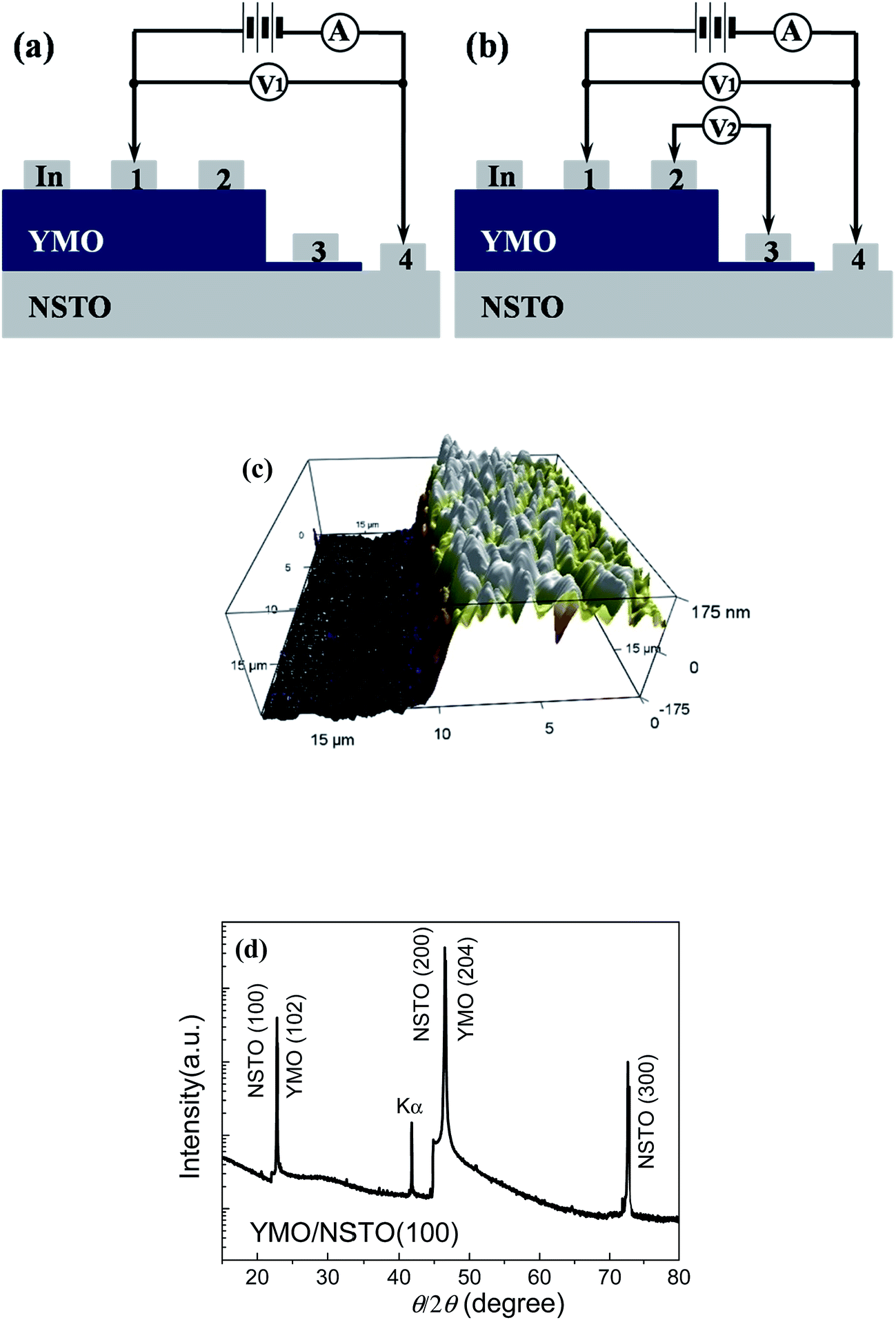 | ||
| Fig. 1 (a) and (b) Measurement schematics for the two-wire and four-wire method. (c) 3D AFM image of the step of YMO layer. (d) X-ray θ–2θ pattern of the YMO/NSTO thin film. | ||
The structure of YMO film was examined by a Bruker D8 advance X-ray diffraction (XRD) instrument. The I–V characteristics were measured by a Keithley 2400 and 2182 system. The impedance spectra were investigated using an Agilent 4294A precision impedance analyzer. The thickness, surface morphology and piezoelectric properties of the YMO step film were studied by two atomic force microscopy (AFM) systems produced by Oxford Instruments and Bruker. The Positive Up Negative Down (PUND) measurements of the YMO/NSTO device were carried out by a ferroelectric test system (Workstation, Radiant Technologies. Inc., USA). No special statement measurements were conducted at room temperature.
Results and discussion
The 3D image (Fig. 1(c)) of YMO step film observed by AFM indicated that the step with 350 nm thickness formed through the sample was partially covered by the mask after deposition for 180 s. However, the cross-section images in Fig. S1 of ESI† (SM) observed by a JSM-7001F scanning electron microscope (SEM) show that the YMO layer thickness under pad 2 and pad 3 are about 330 nm and 60 nm, respectively. Because of the stacking near the edge of the mask, the thickness measured by AFM is bigger than the value measured by SEM far away from the edge of the mask. The θ–2θ XRD pattern in Fig. 1(d) shows that only YMO (102) and (204) peaks were observed in addition to the STO (00l) reflections. It indicates that the YMO film shows a good oriented growth with the hexagonal structure.In order to characterize the layer and the interface, impedance spectra (Fig. 2(a)) were obtained in 2-to-3-electrode configuration and 1-to-4-electrode configurations. The inset is the equivalent circuit diagrams. The YMO/NSTO device was represented by two semicircles, which are modeled as two parallel RC circuits. However, the YMO layer resulted in one small semicircle, which is modeled by one parallel RC circuit. It is clear that the YMO/NSTO device includes two inhomogeneous regions, namely, the YMO layer and the YMO/NSTO interface. The impedance spectra indicate that the total resistance (Rt) of the device can be equivalent to the resistance of the YMO layer (Rl) in series with the resistance of the YMO/NSTO interface (Ri).
 | ||
| Fig. 2 (a) Impedance spectra of the YMO layer and YMO/NSTO device measurement. The inset is the equivalent circuit diagrams for 1-to-4-electrode and 2-to-3-electrode configurations. (b) I–V curve after applying voltage-sweep as 0 V → +1 V → −1 V → 0 V of the YMO/NSTO device. The inset shows the I–V curves indicating ohmic contacts for the top and bottom electrodes. (c) The RS behaviors after applying different voltage-sweeps 0 → +Vmax → −Vmax → 0 V. The inset shows the RHRS/RLRS ratio as a function of write amplitude. (d) Schematic of the pulse train to measure the RHRS/RLRS ratio of the YMO/NSTO device. (e) The RS behaviors were measured using the four-wire method with current-sweep cycle as +Imin → +Imax → −Imax → −Imin. RS behaviors of the YMO layer and the YMO/NSTO device are denoted by the red and black line. (f) Retention properties of YMO/NSTO device and YMO layer at 100 °C (write voltage = ±3.5 V). (g) Endurance behaviors of the YMO/NSTO device and YMO layer at room temperature (write voltage = ±3.5 V). (h) Top electrode areas dependence of the HRS and LRS for the YMO/NSTO and YMO layer, respectively. | ||
Using the two-wire (Fig. 1(a)) or four-wire (Fig. 1(b)) measurement, the RS of the YMO layer and YMO/NSTO interface can be measured together or independently. A Keithley 2400 sourcemeter can be equivalent to an ampere meter (A) in series and a voltmeter (V1) in parallel with the power supply by two-wire method. To distinguish the RS of the layer from that of device, a Keithley 2182A nano-voltage meter (V2) was added in the four-wire method. The voltage (V1) between 2 and 3 electrodes directly corresponds to Rl and the voltage (V2) between 1 and 4 corresponds to Rt, i.e., Ri plus Rl. In previous reports, there are some similar methods to distinguish the layer resistance from the interface resistance.15,16 The point of showing the switching by voltage separately is to synchronously, independently, and accurately investigate the resistance changes of the YMO layer and the YMO/NSTO interface during RS process. The purpose of this approach is to further clarify the origin of the RS in the YMO/NSTO device.
To rule out the influence of electrodes and form good ohmic contacts, indium (In) top electrodes (the inset of Fig. 2(b)) were spurted on the YMO film. To avoid I1,4 > I2,3, the In top electrode was masked into strips perpendicularly to the direction of the current. The bottom In electrode was soldered on the back of NSTO substrate. A positive electrical field is defined as the current flowing from the top to the bottom electrode. As shown in Fig. 2(b), the I–V curve of YMO/NSTO device at the low voltage scan as 0 V → +1 V → −1 V → 0 V shows typical rectification characteristics.
By increasing write voltage amplitude, such as 2.0, 2.5, 3.0, 3.5, 4.0, 4.5, and 5.0 V, a group of bipolar RS I–V curves were measured, as shown in Fig. 2(c), using two-wire V-source measurement. The plots with semilogarithmic coordinate showed a clear opening of hysteresis. RLRS and RHRS represent the R values of low resistance states (LRS) and high resistance states (HRS) of the YMO/NSTO device, respectively. The RHRS/RLRS ratio was measured using a pulse train shown schematically in Fig. 2(d). The measurement starts from an unpolarized state. At a certain write voltage, pairs of write pulses with opposite polarities were applied. The inset in Fig. 2(c) shows the ratio calculated through the currents, which were collected by −0.5 V read pulses (gray color) after the positive (red color) and negative (blue color) write pulses in Fig. 2(d). The write voltage dependence of the RHRS/RLRS ratio is also shown in the inset of Fig. 2(c). A further discussion combined with ferroelectric will be carried on in the following text.
The RS behaviors of the YMO/NSTO device and the YMO layer were measured independently using the four-wire method. As shown in Fig. 2(e), a current sweep in the +Imin → +Imax → −Imax → −Imin scan cycle was applied from 1 to 4 electrodes. The Rt and Rl both switched from HRS to LRS in the +Imin → +Imax process and from the LRS to the HRS in the −Imax → −Imin process. In the +Imax → −Imax process, they both maintain LRS.
The RS of YMO layer can obviously be observed in Fig. 2(e). The magnitude order of initial Rt (Rt = V1/I) of the YMO/NSTO device was about 105 Ω, whereas the Rl (Rl = V2/I) of the YMO layer was about 104 Ω. During the SET (from HRS to LRS) process, the Rt decreased from 105 Ω to 102 Ω and the Rl also switched from 104 Ω to 101 Ω. During the RESET (from LRS to HRS) process, the Rt increased from 102 Ω to 106 Ω and the Rl also switched from 101 Ω to 103 Ω. Similar behaviors were also observed in other cells in this sample. The results indicate that with the increasing applied current, the RS takes place near the YMO/NSTO interface and in YMO layer synchronously. Although the amplitude of the RS in YMO layer is substantially smaller than that of YMO/NSTO interface, the RS in the YMO layer has potential applications in precise RS devices with low power consumption because the voltage and current of RS for the YMO layer are much lower than those for the interface of YMO/NSTO.
Fig. 2(f) and (g) show the retention and reproducibility properties for the YMO/NSTO device and the YMO layer, respectively. There was no significant reduction within 14 h at 100 °C. This indicates that the device has a stable retentivity in the high temperature environment. The RHRS/RLRS ratios ∼ 1000 times (YMO/NSTO device) and ∼500 times (YMO layer) were maintained over 100 cycles. These factors indicate the long retention and good endurance of the YMO/NSTO device and the YMO layer, which are the promising candidates for non-volatile resistive multi-level memories.
Investigating the area-dependence of RS is an effective method for distinguishing between filamentary mechanism and interfacial effect. In Fig. 2(h) of SM, the HRS and LRS of YMO/NSTO device and YMO layer significantly increase with decreasing electrode areas, thus excluding the filamentary mechanism.
During the abovementioned experiment, the current compliance (10 mA) was set to protect the sample from complete breakdown. To exclude switching by Joule heating, the RS at low temperature (77 K) in the liquid nitrogen condition was obtained, as shown in Fig. 3S.† The compliance current (Ic) was set to 10 mA (300 K) and 1 mA (77 K), respectively. Because the provided electrical power (V × I) at 77 K is much lower than at 300 K, the Joule heating of the YMO/NSTO device was largely reduced. If the RS behavior originated from Joule heating, the RS behavior at low temperature and low electrical power will be weakened or vanished. However, the switching is always obvious and the HRS of the YMO/NSTO device is dropped further after RS. Therefore, the RS mechanism of Joule heating can be excluded.
To explore the origin of the RS behavior of the YMO/NSTO ferroelectric device, piezoresponse force microscopy (PFM) was performed. Fig. 3(a) shows the topography of the YMO film on the NSTO substrate with an area of 1.5 × 1.5 μm2. The film exhibits 3D islands randomly nucleated on the flat surface with a root-mean-square roughness of about 1.48 nm. The poly-domain architecture can be observed in the out of plane (OP)-PFM images in Fig. 3(b) and (c) before poling. In general, the section analysis in Nanoscope Analysis of the AFM program proves most useful for making direct depth measurements of the surface features. When a line is drawn on the image, the cross section is displayed directly. To prove that the OP-PFM image is not linked to the topography of the YMO film, we used the section command in three same positions represented by red, green and blue horizontal lines in the height (see Fig. 3(a)) and phase (see Fig. 3(b)) images of YMO film. The cross section figures (see Fig. 4S†) were drawn using the same corresponding colors. Some piezoelectric domains were differently oriented in the same grain. On the other hand, several grains were involved in one piezoelectric domain. Moreover, grains and domains were looked without any dependencies. Therefore, we can deduce that the OP-PFM image is not linked to the topography of the YMO film.
 | ||
| Fig. 3 (a) Surface morphology of the YMO film; (b) OP-PFM phase image; (c) OP-PFM amplitude image; (d) OP-PFM phase image after poling processes. (e) OP-PFM amplitude image after poling processes. (f) OP-PFM phase hysteresis loop: top, phase signal; bottom, amplitude signal. | ||
Fig. 3(d) and (e) show the OP-PFM phase and amplitude images of ferroelectric domains written on the YMO surface. A 2 × 2 μm2 area was poled upward with a voltage +6 V, in which a 1 × 1 μm2 area was poled downward with a voltage of −6 V. The 180° phase contrast shows that the polarizations are antiparallel in the two domains. The OP-PFM hysteresis loops shown in Fig. 3(f) indicate the ferroelectric nature of the YMO film. The local coercive voltages are approximately ±2 V, as indicated by the minimum of the amplitude loop. The OP polarization was reversed effectively when the bias voltage was swept from −10 V to 10 V. In addition, a slight off set of the PFM hysteresis loop was observed, which could be due to the presence of an internal built-in electric field.17
The external electric field can lead to ferroelectric-like behavior due to surface charges and interfacial electrons trapping, which may lead to an error in information storage. For an example, bulk STO is not a ferroelectric material; however, its surface was previously reported to exhibit ferroelectric-like behavior due to the electrical transport properties of graphene.18 Because the ferroelectric-like behaviors depend on the electric field, if the external electric field is removed, the ferroelectric-like behaviors will disappear. Therefore, the PFM images of YMO/NSTO device were measured after poling processes every several hours in Fig. 4.
 | ||
| Fig. 4 (a)–(d) OP-PFM phase image after the poling processes every few hours, (a) just after poling; (b) after 6 h; (c) after 12 h; (d) after 24 h. (e)–(h) OP-PFM amplitude image after the poling processes every few hours. (e) Just after poling; (f) after 6 h; (g) after 12 h; (h) after 24 h. | ||
Fig. 4 shows that the boundary of the two colors in OP-PFM phase images become hazy with time after poling processes. We believe that there are two main reasons for the disappearance of the phase images. One is the effect of trapped charges, and the other was the ferroelectric depolarization. Because the trapped charges effect depends on the electric field, after the external electric field is removed, the ferroelectric-like behaviors should disappear immediately. However, the depolarization will make the images after the poling process slowly fade away. Based on the abovementioned consideration, we believed that the behaviors observed in Fig. 3 and 4 originated from the ferroelectric properties of the YMO film and not from the effect of trapped charges.
To further investigate the ferroelectric properties of the YMO film, the PUND data of the YMO/NSTO device were measured by the ferroelectric test system, as shown in Fig. 4S.† PUND is a standard ferroelectric measurement, which consists of five pulses. The test can provide two PUND parameters, one at the maximum applied voltage and the other at zero volts. The maximum polarization (Pmax) and the remanent polarization (Pr) can be obtained from the data of the PUND measurements. In Fig. 4S,† the PUND result indicates that Pmax and Pr increase with increasing voltages. This is because the high electrical field provides high energy, which produces the “electrical driving force” to the electric dipole moments in the YMO film. When the voltage is stronger than 2 V (ferroelectric coercive voltage), the increase in Pmax and Pr becomes slow, indicating the polarization is near saturation. This matches with the RS behaviors and PFM results of the YMO/NSTO device.
Considering the result mentioned above, the relationship between the RS behavior and the ferroelectric of the YMO/NSTO device is illustrated with the energy band diagrams in Fig. 5(a) and (b). For a NSTO (0.7 wt%) single crystal, it is usually treated as a n-type semiconductor with a band gap of 3.2 eV.19 YMO film exhibits p-type semi-conductivity with a band gap of 1.5 eV.20–23 Therefore, a p–n junction can be formed near the YMO/NSTO interface. If the ferroelectric polarization points to NSTO, positive bound charges in the YMO/NSTO interface will drive the electrons on the surface of NSTO into accumulation.24,25 As shown in Fig. 5(a), when the positive voltage is applied to the YMO/NSTO device, the positive polarization bound charges aggregate at the YMO/NSTO interface. Moreover, the electron carriers represented by “dot” symbols in n-type NSTO are attracted by these positive bound charges and migrated toward the interface, resulting in a decrease in the depletion width. Therefore, the electrons would transfer from NSTO to YMO and the sample is then set to a LRS. However, when the negative voltage amplitude larger than the coercive bias was applied, the polarization will be reversed, pointing to a YMO film, as shown in Fig. 5(b). The electron carriers in n-type NSTO are repelled by the negative bound charges at the YMO/NSTO interface. As a result, the negative ferroelectric bound charges were screened by the immobile ionized donors25,26 represented by “circle plus” symbols and then the depletion width increased. Therefore, the energy barrier between YMO and NSTO would hinder the transport of electrons, which results in HRS.27,28
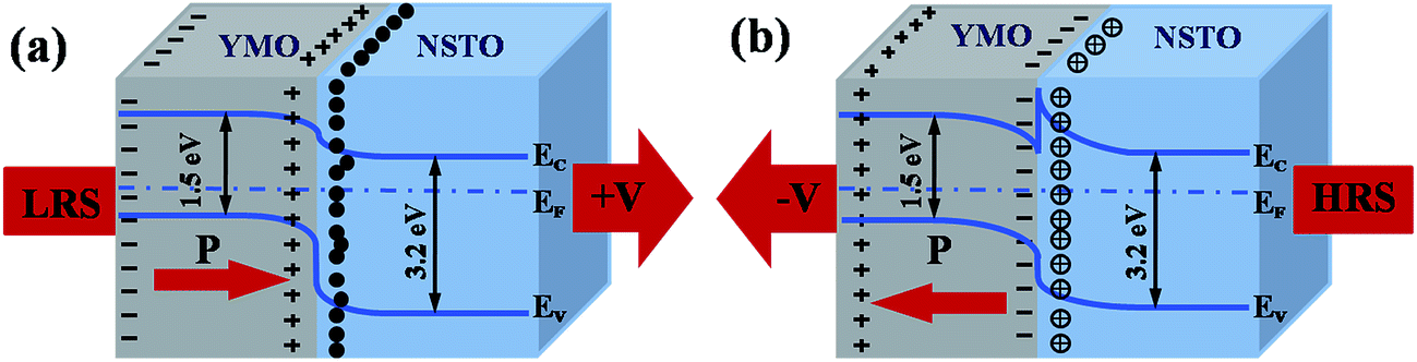 | ||
| Fig. 5 Schematic and energy band diagram of the YMO/NSTO device. LRS (a) and HRS (b) caused by the corresponding polarization directions in parallel to the polarity of the external voltage. | ||
The ferroelectric polarization corresponds to the change of RHRS/RLRS ratio, which is observed in Fig. 2(c). At low write voltages, such as 1 V and 1.5 V, the RHRS/RLRS ratio is close to unity, because neither the positive nor negative voltage is strong enough to make a ferroelectric reversal. When the applied voltages are greater than ±2 V (the coercive voltage), the LRS saturates with increasing the positive write amplitude. Because of the existence of the compliance current, the largest voltage indeed was provided up to 2.4 V. Therefore, the positive side remains roughly same. However, the hysteresis towards negative sweeping voltage becomes wider. This is because the currents are smaller than the compliance current (10 mA) and the negative voltages provided on the sample are not limited. The HRS increases exponentially, due to the increase in depletion width in the p–n junction. The charge transmittance depends exponentially on the barrier width according to the basic quantum mechanism.29 Therefore, the RHRS/RLRS ratio increases continuously with further increase in write amplitude. Similar results were reported for the Pt/BTO/NSTO heterostructure.30 After 24 hours, the OP-PFM phase and amplitude images of ferroelectric domains written on the YMO surface have obvious 180° phase contrasts in Fig. 4 revealing the real ferroelectric behavior and excluding the possibility of the ferroelectric-like behavior. The RS of the YMO layer under the modification of ferroelectric polarization may be associated with changes in the crystal structure and stoichiometry due to the applied external electric field.31 According to the analysis mentioned above, it can be concluded that the modification of the interface induced by polarization reversal is responsible for the RS behaviors in the YMO/NSTO device.
Conclusions
The YMO/NSTO device with a step exhibits a large RHRS/RLRS ratio (>1000 times), high endurance (>100 cycles), long retention (>14 h at 100 °C) and more than four-level operation. The RS behaviors of the YMO layer can be distinguished from the YMO/NSTO device and it could be applied in precise RS devices with low power consumption. The multilevel RS behaviors in the YMO/NSTO device can be explained on the basis of polarization reversal-induced modification of the width of the depletion region at the p–n interface.Acknowledgements
This study was supported by the National Natural Science Foundation of China (61350012 and 60976016), the Foundation of He'nan Educational Committee (12A480001), and the Program for Innovative Research Team in Science and Technology in University of Henan Province (IRTSTHN) (Grant No. 2012 IRTSTHN004).References
- J. Borghetti, G. S. Snider, P. J. Kuekes, J. J. Yang, D. R. Stewart and R. S. Williams, Nature, 2010, 464(7290), 873 CrossRef CAS PubMed.
- J. J. Yang, D. B. Strukov and D. R. Stewart, Nat. Nanotechnol., 2013, 8(1), 13 CrossRef CAS PubMed.
- S. Gao, F. Zeng, M. J. Wang, G. Y. Wang, C. Song and F. Pan, Phys. Chem. Chem. Phys., 2015, 17, 12849 RSC.
- H. D. Kim, M. J. Yun, J. H. Lee, K. H. Kim and T. G. Kim, Sci. Rep., 2014, 4, 4614 Search PubMed.
- Y. Bai, H. Q. Wu, R. Wu, Y. Zhang, N. Deng, Z. P. Yu and H. Qian, Sci. Rep., 2014, 4, 5780 CAS.
- A. Rana, H. Lu, K. Bogle, Q. Zhang, R. Vasudevan, V. Thakare, A. Gruverman, S. Ogale and N. Valanoor, Adv. Funct. Mater., 2014, 24(25), 3962 CrossRef CAS.
- A. Bogusz, A. D. Müller, D. Blaschke, I. Skorupa, D. Bürger, A. Scholz, O. G. Schmidt and H. Schmidt, AIP Adv., 2014, 4(10), 107135 CrossRef.
- N. Jiang, S. M. Woodley, C. Richard, A. Catlowc and X. Zhang, J. Mater. Chem. C, 2015, 3(18), 4787 RSC.
- Y. Du, X. L. Wang, D. P. Chen, Y. X. Yu, W. C. Hao, Z. X. Cheng and S. X. Dou, Phys. Chem. Chem. Phys., 2013, 15, 20010 RSC.
- T. Choi, Y. Horibe, H. T. Yi, Y. J. Choi, W. Wu and S. W. Cheong, Nat. Mater., 2010, 2632 Search PubMed.
- Z. B. Yan, S. Z. Li, K. F. Wang and J. M. Liu, Appl. Phys. Lett., 2010, 96(1), 012103 CrossRef.
- Z. Chen, C. L. Ma, F. X. Wu, Y. B. Chen, J. Zhou, G. L. Yuan, Z. B. Gu, S. T. Zhang and Y. F. Chen, Appl. Surf. Sci., 2011, 257, 8033 CrossRef CAS.
- A. Tsurumaki, H. Yamada and A. Sawa, Adv. Funct. Mater., 2012, 22, 1040 CrossRef CAS.
- L. Jiang, W. S. Choi, H. Jeen, S. Dong, Y. Kim, M. G. Han, Y. Zhu, S. V. Kalinin, E. Dagotto, T. Egami and H. N. Lee, Nano Lett., 2013, 13, 5837 CrossRef CAS PubMed.
- Y. Tokunaga, Y. Kaneko, J. P. He and T. Arima, Appl. Phys. Lett., 2006, 88, 223507 CrossRef.
- S. Chen, L. P. Chen, G. J. Lian and G. C. Xiong, J. Appl. Phys., 2009, 106, 023708 CrossRef.
- N. Balke, I. Bdikin, S. V. Kalinin and A. L. Kholkin, J. Am. Ceram. Soc., 2009, 92(8), 1629 CrossRef CAS.
- A. Sachs, Z. S. Lin and J. Shi, Sci. Rep., 2014, 4, 3657 Search PubMed.
- L. Zhao, Z. Lu, F. Zhang, G. Tian, X. Song, Z. Li, K. Huang, Z. Zhang, M. Qin, S. J. Wu, X. Lu, M. Zeng, X. Gao, J. Dai and J. M. Liu, Sci. Rep., 2015, 5, 9680 CrossRef CAS PubMed.
- W. Huang, J. J. Yang, G. Y. Gao, Y. Lei, J. Zhu, H. Z. Zeng, F. G. Zheng and J. H. Hao, Appl. Phys. Lett., 2014, 105(6), 062904 CrossRef.
- P. R. Ren, H. Q. Fan and X. Wang, Appl. Phys. Lett., 2013, 103(15), 152905 CrossRef.
- N. Fujimura, H. Sakata, D. Ito, T. Yoshimura, T. Yokota and T. Ito, J. Appl. Phys., 2003, 93, 6990 CrossRef CAS.
- J. E. Medvedeva, V. I. Anisimov, M. A. Korotin, O. N. Mryasov and A. J. Freeman, J. Phys.: Condens. Matter, 2000, 12(23), 4947 CrossRef CAS.
- Y. Du, X. L. Wang, D. P. Chen, S. X. Dou, Z. X. Cheng, M. Higgins, G. Wallace and J. Y. Wang, Appl. Phys. Lett., 2011, 99(25), 252107 CrossRef.
- M. Takizawa, K. Maekawa, H. Wadati, T. Yoshida, A. Fujimori, H. Kumigashira and M. Oshima, Phys. Rev. B: Condens. Matter Mater. Phys., 2009, 79, 113103 CrossRef.
- S. Mathews, R. Ramesh, T. Venkatesan and J. Benedetto, Science, 1997, 276(5310), 238 CrossRef CAS PubMed.
- S. L. Miller and P. J. McWhorter, J. Appl. Phys., 1992, 72(12), 5999 CrossRef CAS.
- X. H. Wei, W. Huang, Z. B. Yang and J. H. Hao, Scr. Mater., 2011, 65(4), 323 CrossRef CAS.
- D. Griffiths, Introduction to Quantum Mechanics, Pearson Prentice Hall, 2005 Search PubMed.
- Z. Wen, C. Li, D. Wu, A. D. Li and N. B. Ming, Nat. Mater., 2013, 12, 3649 CrossRef PubMed.
- A. Morelli, S. Venkatesan, G. Palasantzas, B. J. Kooi and J. Th. M. de Hosson, J. Appl. Phys., 2007, 102(8), 084103 CrossRef.
Footnote |
| † Electronic supplementary information (ESI) available. See DOI: 10.1039/c5ra19986g |
| This journal is © The Royal Society of Chemistry 2016 |