DOI:
10.1039/C5RA19566G
(Paper)
RSC Adv., 2016,
6, 3526-3531
Nonlinear optical effects in nitrogen-doped graphene
Received
22nd September 2015
, Accepted 16th December 2015
First published on 18th December 2015
Abstract
The band structure of graphene can be adjusted by incorporating other elements or functional groups, correspondingly, the response to an external light field will also be changed. In this study, we investigated the nonlinear optical (NLO) responses of N-doped graphene nanosheets (N-Gns) with an open aperture Z-scan method, under the excitation of picosecond laser pulses. To the best of our knowledge, this is the first time that two-photon absorption (2PA) of N-Gns has been reported. The normalized nonlinear transmission demonstrates that with the increasing excitation energy, the saturable absorption (SA) and the 2PA appear successively. Compared to the 532 nm excitation, the 1064 nm excitation exhibits smaller saturable intensity Is and larger 2PA coefficient β. At the same time, the N-Gns present superior NLO property compared to pure graphene. Consequently, N-Gns will be a promising candidate for SA or optical limiting (OL) applications.
Introduction
Owing to its rare and precious properties, such as high optical transparency, flexible mobility, excellent elongation and thermal conductivity,1–5 graphene opened a new nano-world since it was first exfoliated from graphite in 2004.6 Strong intra-layer covalent bonding and weak inter-layer van der Waals interaction allow graphene to form a tough two-dimensional (2D) nanostructure. Due to the unique band structure where the conduction band and the valance band meet at the Dirac point, carbon-based graphene exhibits a number of remarkable optoelectronic properties, which have potential applications in electronics, optics, magnetics, biomedicine, energy storage and other domains. In the past, a large number of studies have been devoted to the electronic properties of graphene,3,5–9 until recent years when people began to pay attention to the optical properties of graphene,1,9 particularly the NLO characteristics of graphene.10–14 SA13,14 and OL effects11,12 over a broad waveband (from visible to infrared) have been found in graphene. SA is the consequence of the Pauli exclusion principle. When the excitation energy reaches the saturation intensity, the photo-excited carriers are saturated and the remaining excitation photons can transparently transmit, i.e. these photons will not be absorbed. Utilizing this property, graphene can serve as the passively saturable absorber in Q-switched or mode-locked lasers.15,16 The mechanism of the OL effect comes from reverse saturable absorption (RSA), multi-photon absorption, and free-carrier absorption (FCA). Utilizing the OL effect of graphene, new laser protecting technology for sensitive optical components and human eyes can be developed in the future.
Nevertheless, the intrinsic zero band gap structure4–6 of graphene brings many limitations for electronic and photonic applications. Doping is an effective method to adjust the band gap and tailor the optoelectronic properties of graphene. Recently, some doped graphenes, such as graphene–polymer,17 graphene/ZnO,18 NH4 functionalized graphene,19 graphene–porphyrin composites,20 have been reported. In 2009, the N-Gns were first synthesized by chemical vapor deposition (CVD) method.21 The doping of N atoms opens the intrinsic zero band gap structure of graphene and leads to a semiconductor-like transition, which greatly expands the applications. In this study, the NLO properties of N-Gns were investigated by the Z-scan technique of picosecond pulse lasers. For the first time, the OL behavior of N-Gns was observed. The results indicate that N-Gns is an excellent NLO material for SA and OL applications.
Characterization
The original powder was purchased from Nanjing XFNANO Materials Tech Co. Ltd. of China. It was synthesized by the CVD method,21–23 based on the oxidation–reduction reaction of graphene oxide and ammonia gas. The electrical conductivity was over 1000 S m−1, and the nitrogen content was 3.0–5.0 at%. To detect the size and the thickness of N-Gns, an atomic force microscopy (AFM) measurement was carried out. The appropriate powder was dissolved in ultrapure water. To enhance the dissolution of the sample, surfactant polyvinylpyrrolidone (PVP) was added with eight times the content of the N-Gns. After ultrasound treatment for two hours at a power of 300 W, the dispersion liquid was prepared completely. A part of the dispersion liquid was stored in a quartz colorimetric utensil of 2 mm thickness for the NLO experiment. The remaining part was dropped on a pre-cleaned quartz substrate, and placed in a vacuum device at room temperature to remove the residual solvent, which was used as the sample for the measurements of basic properties. Fig. 1 shows the AFM image (left) and the thickness profiles (right) of the representative deposited N-Gns. The results reveal that most of the N-Gns have a radial dimension of a few hundred nanometers. About 80% of the N-Gns have a thickness of 5 nm or so. Considering the aggregation effect during the preparation process of the AFM sample, including deposition and drying, the actual thicknesses of N-Gns in dispersion might be less than 5 nm, which indicates that the powder consists of 1–5 atomic layer graphene nanosheets.
 |
| | Fig. 1 Typical AFM image (left) and thickness profiles (right). | |
The result of X-ray photoelectron spectroscopy (XPS) confirms the doping of nitrogen, as shown in Fig. 2. The concentration of nitrogen was calculated to be 1.6 at%. In the manufacturing process, some oxygen element remained in the sample, which was 7.0–7.5 at% due to the incomplete reduction reaction, thus the O 1s peak around 532.0 eV was observed (Fig. 2a). The other peaks at 284.7 and 399.5 eV appeared due to C 1s of sp2 C and N 1s of the doped N, respectively. The N 1s peak (Fig. 2b) consists of three peaks, which indicates that the N atoms exist in graphene in the way of three different bonding structures. According to the ref. 21, the peaks at 398.2 and 399.5 eV originate from the π-conjugated system of N atoms and the difference is the number of p-electrons (corresponding to one and two p-electrons, respectively) that contributed to the π system. The peak at 401.1 eV comes from the substitution of honeycomb C atoms in graphene. The C 1s spectrum (Fig. 2c) is composed of two Lorentzian peaks. The stronger peak at 284.7 eV corresponds to the sp2 C–C band itself, which reflects the honeycomb lattice structure of the pure graphene. The peak at 285.7 eV corresponds to the sp2 C–N, which originates from the substitution of N atoms or the defects of the N-Gns. As shown in Fig. 2d, the O 1s peak can be split into two Lorentzian peaks. The stronger peak at 533.6 eV comes from the sp2 C–O bond and the weaker peak at 531.0 eV is due to the combined actions of C![[double bond, length as m-dash]](https://www.rsc.org/images/entities/char_e001.gif) O, O–CO and O–CO–O bonds.24
O, O–CO and O–CO–O bonds.24
 |
| | Fig. 2 (a) XPS result of N-Gns. (b) N 1s spectrum, (c) C 1s spectrum, and (d) O 1s spectrum. The N 1s peak can be split into three Lorentzian peaks at 398.2, 399.5 and 401.1 eV, which are labeled by red, green, and purple dashed lines, respectively. The C 1s peak can be split into two Lorentzian peaks at 284.7 and 285.7 eV, which are labeled by red and green dashed lines, respectively. The O 1s peak can be split into two Lorentzian peaks at 531.0 and 533.6 eV, which are labeled by green and red dashed lines, respectively. | |
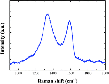
The Raman spectrum of N-doped graphene is shown in Fig. 3 and is very similar to those reported by Anand et al.25 The N doping creates a large amount of topological defects, and the sp2 C of these defects induces the much stronger D band Raman peak at ∼1330 cm−1. On the contrary, for pure graphene, this peak is very faint.25 Thus, the obvious D band Raman peak in Fig. 3 reflects the effective N doping and the increasing of lattice disorder. The G band Raman peak is at 1584 cm−1, which is identical to that of pure graphene.
 |
| | Fig. 3 Raman spectrum of the N-doped graphene. | |
NLO experiment
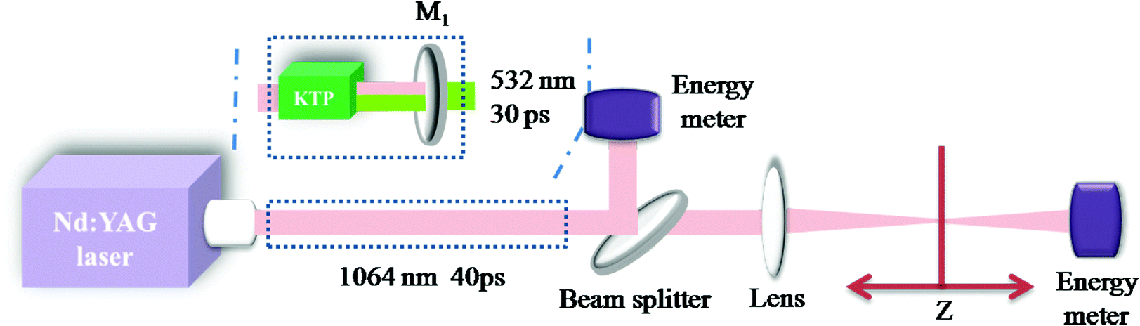
The open aperture Z-scan technique was used to investigate the NLO properties of the as-prepared N-Gns dispersion liquid. As mentioned above, appropriate surfactant PVP was added to enhance the dissolution of the sample. The dispersion was stored in a quartz colorimetric utensil with a thickness of 2 mm. Fig. 4 displays the experimental setup with laser excitations of 1064 and 532 nm. The laser resource was a dye mode-locked Nd:YAG laser operating at 1064 nm, 40 ps pulses, with a 10 Hz repetition rate. A KTP crystal was used to generate the frequency doubling laser of 532 nm with a pulse width of 30 ps. The flat mirror M1 served as the filter of the fundamental laser, which was highly transmissive at 532 nm (T > 80%) and highly reflective at 1064 nm (R > 99.5%). The focal length of the convex lens is 30 cm.
 |
| | Fig. 4 Open-aperture Z-scan experimental setup with 1064 and 532 nm laser excitations. | |
Fig. 5 was the measurement results for 1064 and 532 nm excitations. The sample exhibited SA behavior (single photon absorption) when the excitation energy was weak. Under high excitation energy, with the increasing of excitation intensity, the single photon absorption (1PA) became saturated and the two photon absorption (2PA) followed behind. When the excitation energy increased further, the OL effect became more significant. In the Z-scan experiment, the reducing of normalized linear transmittance, which was induced by the OL effect, could be defined as “OL depth”. Thus, the OL depths were 32% at 1064 nm with 6 μJ excitation and 63% at 532 nm with 12 μJ excitation, as shown in Fig. 5. The SA threshold at 1064 nm excitation was 4.1 mJ cm−2, which was much lower than the value at 532 nm excitation (8.5 mJ cm−2). The relatively weaker SA threshold indicates superiority as a saturable absorber at infrared waveband. As the reference, no NLO effects were observed from the PVP water solution without N-Gns.
 |
| | Fig. 5 Open-aperture Z-scan results of N-Gns dispersion with excitation wavelength at (a) 1064 and (b) 532 nm (the discrete points are experimental data and the solid lines are the fitted curves). Insets: schematic diagrams for the energy level transitions of 1PA and 2PA in N-Gns. | |
The insets in Fig. 5 display the schematic diagrams for the energy level transitions of 1PA and 2PA in N-Gns. The SA effect is the consequence of the 1PA process. Under the excitation of an external laser, the electrons jump to the conduction band from the valence band, and subsequently cool down within the constraint of Pauli exclusion principle. When the incident intensity reaches the saturation intensity, the photo-carrier intensity is saturated and the remaining photons transparently pass through, i.e. these photons are not absorbed. As shown in the insets in Fig. 5, to achieve the SA effect, the long-wavelength photon excitation requires a lower intensity to completely fill the lower energy levels compared to a short-wavelength photon excitation. When the excitation energy is increased further, two excitation photons tangle together and the electrons are stimulated to much higher energy levels. Accordingly, the transmittance declines rapidly. From the insets in Fig. 5, it can be seen that for 2PA, the long wavelength excitation of 1064 nm corresponds to smaller energy band volume, compared to the short wavelength excitation of 532 nm. This means that the 2PA of 1064 nm excitation corresponds to fewer energy levels, i.e. fewer absorbed photon numbers. The small single photon energy and few absorbed photon numbers indicate that the 2PA threshold of 1064 nm excitation is obviously lower than that of 532 nm excitation; at the same time, the 2PA adjusting depth of 1064 nm excitation is smaller, which agrees with the experimental results demonstrated in Fig. 6. From this figure, it can be seen that for each excitation there are three different NLO stages. For 1064 nm excitation (Fig. 6a), when the excitation energy varies from 4.1 to 12.6 mJ cm−2, the SA is the dominant NLO effect. When the excitation energy is in the range of 12.6–33.9 mJ cm−2, the SA and the OL effects co-exist. When the excitation energy exceeds 33.9 mJ cm−2, the OL behavior becomes the main NLO effect. For 532 nm excitation, these three stages correspond to the excitation energy of less than 34.0 mJ cm−2, that in the range of 34.0–69.8 mJ cm−2, and that beyond 69.8 mJ cm−2, respectively (Fig. 6b). In Fig. 6, we used the transmittance variation of 1% as the distinguishing criterion of different stages. When the transmittance increased to 101% of the starting linear transmittance value 1 and thereafter continued to increase, we set the corresponding energy fluence as the SA threshold. When the transmittance decreased to 99% of the highest transmittance, the corresponding interval range of energy fluence was set as the coexistence region of SA and OL. Thus, the SA region and OL region could be determined. The experimental results illustrate that by appropriately controlling the laser energy density, N-Gns can be selected to be the SA material or the OL material. The former can be used in passively mode-locking and Q-switching, and the latter can be used to protect human eyes or sensitive optical components from laser-induced damage.
 |
| | Fig. 6 Three different NLO stages including SA and OL behaviors with excitation at (a) 1064 and (b) 532 nm. | |
Discussion
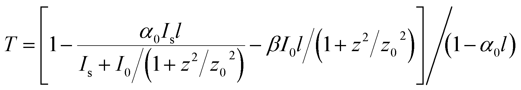
The normalized transmittance in the Z-scan measurement can be expressed by eqn (1), where α and α0 are the total and linear absorption, respectively, and l is the sample length. The same linear absorption coefficient α0 of 2.23 cm−1 was measured at both 1064 and 532 nm. The excitation intensity I(z) is determined by the peak intensity I0 at z = 0, the Rayleigh length z0 of the beam and the position z of the sample (eqn (2)). For a system in which SA and 2PA co-exist,17,26 the total absorption α(I) can be described by eqn (3), where β is the 2PA coefficient and Is is the saturable intensity, defined as the optical intensity when the optical absorbance is reduced to one half of its unbleached value. The first and the second terms on the right side of eqn (3) represent the SA and the 2PA, respectively. Combining eqn (1)–(3), the normalized transmittance can be expressed as eqn (4), which is used to fit the Z-scan experimental data.| | |
T = (1 − αl)/(1 − α0l)
| (1) |
| | |
I(z) = I0/(1 + z2/z02)
| (2) |
| |
 | (3) |
| |
 | (4) |
The theoretical fitting curves are plotted in Fig. 5 along with the experimental points. It can be seen that they present perfect agreements. For 1064 nm excitation, the saturable intensity Is and the 2PA coefficient β are fitted to be 0.35 GW cm−2 and 0.76 cm GW−1, respectively. For 532 nm excitation, Is and β are fitted to be 0.87 GW cm−2 and 0.46 cm GW−1, respectively. The lower Is at 1064 nm excitation indicates that a long wavelength laser (such as infrared light) can easily realize the SA in N-Gns, which can be used in passively mode-locked lasers. This property is promising for changing the current research situation of solid-state lasers, i.e. with the infrared laser (particularly the far infrared laser), it is difficult to reach high energy output.27,28 At the same time, the 2PA coefficient β of N-Gns significantly increases as the wavelength increases, which implies excellent sensitivity and good OL effect for an infrared laser. In many previous studies on two-dimensional materials, the β at 1064 nm is often smaller than that at 532 nm. There are also some contrary examples which are consistent with the present result, such as functionalized multilayer graphene (fG),29 graphene nanoribbons (GNRs) and graphene oxide nanoribbons (GONRs).12 We speculate that the relative magnitude of β at different wavelengths will be related to the content of N. As introduced at the beginning of the “Characterization” part, we only have one type of N-Gns sample at hand. Maybe in the future more abundant results about β at different wavelengths could be obtained, when more samples with different N contents are available.
For 1064 and 532 nm excitations, the absorption cross-section σ(σ = ħωβ/N0, where ħω is the excitation photon energy and N0 ≈ 5 × 1016 cm−3 is the density of the N-Gns sample in ultrapure water) is calculated to be 2.8 × 10−45 and 3.4 × 10−45 cm4 s per photon, respectively. These values are comparable to the value of double-decker Pr[Pc(OC8H17)8]2 rare earth complex.30 In addition, we measured the nonlinear transmission of pure graphene under the same experimental conditions. For 1064 and 532 nm excitations, the N-Gns exhibited stronger NLO effects, as shown in Fig. 7. Under the present experimental conditions, we did not observe an obvious SA phenomenon from pure graphene. Although it has been a well-known property of graphene, some previous open Z-scan experiments of graphene have not observed SA phenomenon, either.12,31–33 The reason might come from the experimental condition, sample concentration, and the quality of graphene. The fitted 2PA coefficient of pure graphene is 0.59 and 0.40 cm GW−1 at 1064 and 532 nm, which are smaller than the values of N-Gns (0.76 and 0.46 cm GW−1). As demonstrated in the inset of Fig. 7, the doping of N atoms in graphene opens the zero band gap and decreases the energy band volume,21 correspondingly the threshold of nonlinear absorption is reduced. The experiment proves the superiority of N-Gns for NLO applications.
 |
| | Fig. 7 Nonlinear transmissions of pure graphene and N-Gns under the same energy excitations of 6 μJ at 1064 nm (left) and 12 μJ at 532 nm (right) (the points are the experimental data and the solid lines are the fitted curves). Insets: schematic diagram for the energy level transitions of pure graphene and N-Gns. | |
The imaginary part of the third-order NLO susceptibility, Imχ(3), is directly related to the 2PA coefficient β. Their relationship can be expressed as
| |
 | (5) |
where
c is the light speed in vacuum,
n0 is the linear refractive index and
ω is the angular frequency of the excitation light. The figure of merit (FOM) for the third-order optical nonlinearity is defined as FOM = |Im
χ(3)/
α0|. Referencing the above mentioned results, Im
χ(3) and FOM of N-Gns are calculated to be 1.30 × 10
16 m
3 (sW)
−1 and 5.8 × 10
13 m
4 (sW)
−1 for 1064 excitation and 1.57 × 10
16 m
3 (sW)
−1 and 7.0 × 10
13 m
4 (sW)
−1 for 532 nm excitation, respectively.
Conclusion
For N-Gns that consist of 1–5 atomic layers, the XPS measurement confirms the existence of N atoms, which exhibits three different bond structures. An open-aperture Z-scanner is adapted to detect the NLO properties, including SA and OL effects at different excitation wavelengths and energies. In comparison, the NLO characteristic of N-Gns is proved to be superior to that of pure graphene. This indicates that the N-Gns will be a good substitute for pure graphene in the optoelectronic field, especially for NLO applications.
Acknowledgements
This study was supported by the National Natural Science Foundation of China (Grant No. 61178060) and Natural Science Foundation for Distinguished Young Scholar of Shandong Province (2012JQ18).
Notes and references
- R. R. Nair, P. Blake, A. N. Grigorenko, K. S. Novoselov, T. J. Booth, T. Stauber, N. M. R. Peres and A. K. Geim, Science, 2008, 320, 1308 CrossRef CAS PubMed.
- Z. H. Ni, H. M. Wang, J. Kasim, H. M. Fan, T. Yu, Y. H. Wu, Y. P. Feng and Z. X. Shen, Nano Lett., 2007, 7(9), 2758–2763 CrossRef CAS PubMed.
- X. Du, I. Skachko, A. Barker and E. Y. Andrei, Nat. Nanotechnol., 2008, 3, 491 CrossRef CAS PubMed.
- K. S. Kim, Y. Zhao, H. Jang, S. Y. Lee, J. M. Kim, K. S. Kim, J. H. Ahn, P. Kim, J. Y. Choi and B. H. Hong, Nature, 2009, 457, 706 CrossRef CAS PubMed.
- A. A. Balandin, S. Ghosh, W. Z. Bao, I. Calizo, D. Teweldebrhan, F. Miao and C. N. Lau, Nano Lett., 2008, 8, 902 CrossRef CAS PubMed.
- K. S. Novoselov, A. K. Geim, S. V. Morozov, D. Jiang, Y. Zhang, S. V. Dubonos, I. V. Grigorieva and A. A. Firsov, Science, 2004, 306, 666 CrossRef CAS PubMed.
- J. M. B. Lopes dos Santos, N. M. R. Peres and A. H. Castro Neto, Phys. Rev. Lett., 2007, 99, 256802 CrossRef CAS PubMed.
- A. B. Kuzmenko, E. van Heumen, F. Carbone and D. van der Marel, Phys. Rev. Lett., 2008, 100, 117401 CrossRef CAS PubMed.
- F. Bonaccorso, Z. Sun, T. Hasan and A. C. Ferrari, Nat. Photonics, 2010, 4, 611 CrossRef CAS.
- A. R. Wright, X. G. Xu, J. C. Cao and C. Zhang, Appl. Phys. Lett., 2009, 95, 072101 CrossRef.
- J. Wang, Y. Hernandez, M. Lotya, J. N. Coleman and W. J. Blau, Adv. Mater., 2009, 21, 2430 CrossRef CAS.
- M. Feng, H. B. Zhan and Y. Chen, Appl. Phys. Lett., 2010, 96, 033107 CrossRef.
- Z. W. Zheng, C. J. Zhao, S. B. Lu, Y. Chen, Y. Li, H. Zhang and S. C. Wen, Opt. Express, 2012, 20, 23201 CrossRef CAS PubMed.
- F. Zhang, S. Han, Y. Liu, Z. P. Wang and X. G. Xu, Appl. Phys. Lett., 2015, 106, 091102 CrossRef.
- Q. L. Bao, H. Zhang, Y. Wang, Z. H. Ni, Y. L. Yan, Z. X. Shen, K. P. Loh and D. Y. Tang, Adv. Funct. Mater., 2009, 19, 3077 CrossRef CAS.
- J. Ma, G. Q. Xie, P. Lv, W. Gao, P. Yuan, L. Qian, U. Griebner, V. Petrov, H. Yu, H. Zhang and J. Wang, Sci. Rep., 2014, 4, 1 Search PubMed.
- S. Husaini, J. E. Slagle, J. M. Murray, S. Guha, L. P. Gonzalez and R. G. Bedford, Appl. Phys. Lett., 2013, 102, 191112 CrossRef.
- Q. Y. Ouyang, Z. Xu, Z. Y. Lei, H. W. Dong, H. L. Yu, L. H. Qi, C. Y. Li and Y. J. Chen, Carbon, 2014, 67, 214 CrossRef CAS.
- G. S. Kumar, R. Roy, D. Sen, U. K. Ghorai, R. Thapa, N. Mazumder, S. Sahab and K. K. Chattopadhyay, Nanoscale, 2014, 6, 3384 RSC.
- M. B. Krishna, V. P. Kumar, N. Venkatramaiah, R. Venkatesan and D. N. Rao, Appl. Phys. Lett., 2011, 98, 081106 CrossRef.
- D. C. Wei, Y. Q. Liu, Y. Wang, H. L. Zhang, L. P. Huang and G. Yu, Nano Lett., 2009, 9, 1752 CrossRef CAS PubMed.
- K. S. Kim, Y. Zhao, H. Jang, S. Y. Lee, J. M. Kim, K. S. Kim, J. Ahn, P. Kim, J. Choi and B. H. Hong, Nature, 2009, 457, 706 CrossRef CAS PubMed.
- A. Reina, X. T. Jia, J. Ho, D. Nezich, H. Son, V. Bulovic, M. S. Dresselhaus and J. Kong, Large Area, Nano Lett., 2009, 9, 30 CrossRef CAS PubMed.
- F. Han, S. M. Yang, W. X. Jing, Z. D. Jiang, H. Liu and L. Li, Appl. Surf. Sci., 2015, 345, 18 CrossRef CAS.
- B. Anand, R. Podila, A. M. Rao, R. I. Philip and S. Sai, AIP Conf. Proc., 2013, 1536, 735 CrossRef CAS.
- N. K. M. Naga Srinivas, S. Venugopal Rao and D. Narayana Rao, J. Opt. Soc. Am. B, 2003, 20, 2470 CrossRef.
- H. Zhan, Z. G. Zhou, J. L. He and A. X. Lin, Opt. Lett., 2012, 37, 3408 CrossRef CAS PubMed.
- L. Wang, H. T. Huang, D. Y. Shen, J. Zhang, H. Chen, Y. Wang, X. Liu and D. Y. Tang, Opt. Express, 2014, 22, 19495 CrossRef PubMed.
- B. S. Kalanoor, P. B. Bisht, S. A. Ali, T. T. Baby and S. Ramaprabhu, J. Opt. Soc. Am. B, 2012, 29, 669 CrossRef CAS.
- J. L. Wu, B. Gu, N. Sheng, D. H. Liu and Y. P. Cui, Appl. Phys. Lett., 2014, 105, 171113 CrossRef.
- J. Wang, Y. Hernandez, M. Lotya, J. N. Coleman and W. J. Blau, Adv. Mater., 2009, 21, 2430 CrossRef CAS.
- L. Yan, Y. Xiong, J. Si, X. Sun, W. Yi and X. Hou, Opt. Express, 2014, 22, 31836 CrossRef CAS PubMed.
- B. Anand, A. Kaniyoor, S. S. Sai, R. Philipc and S. Ramaprabhu, J. Mater. Chem. C, 2013, 1, 2773 RSC.
|
| This journal is © The Royal Society of Chemistry 2016 |
Click here to see how this site uses Cookies. View our privacy policy here.