A direct synthesis of Si-nanowires on 3D porous graphene as a high performance anode material for Li-ion batteries
Fethullah Güneş
Department of Materials Science and Engineering, Faculty of Engineering and Architecture, Izmir Katip Celebi University, Cigli-Izmir, 35620 Turkey. E-mail: fethullah.gunes@ikc.edu.tr
First published on 21st December 2015
Abstract
Silicon nanowires (SiNWs) have been successfully synthesized on a three-dimensional porous graphene foam (GF) via chemical vapor deposition (CVD). The unique porous nanoarchitecture of the three-dimensional graphene network enhances the electrical conductivity and provides improved Si-mass loadings. The obtained GF/SiNWs composite, with Si mass loadings of >0.3 mg cm−2 shows high gravimetric and areal capacities, as well as comparable cycle life as an anode material in Li-ion battery. An alumina coating (ALD) of SiNWs also improved the cycle life and rate capability. This facile direct synthesis method of a 3D porous architecture of the GF/SiNWs composite demonstrates a new approach to improve the electrochemical performances of Si-based anode materials for Li-ion batteries.
Introduction
The rapid development of modern society requires energy storage devices with a high energy/power density, long cyclic life and also miniaturization. Rechargeable Li-ion batteries (LIBs) have drawn great attention due to their potential applications in plug-in hybrid electric vehicles, portable electronics as well as integrated microsystems.1–8 Among all the kinds of different anode materials, silicon (Si) has become one of the most promising candidates owing to its high lithium storage capacity of 3572 mA h g−1 at room temperature.9 Yet, dramatic volume change during lithiation/delithiation processes causes electrical disconnection from current collectors and hence capacity fading, which is making this material impractical.10,11 Recently, tremendous efforts have been made to overcome this issue through: (i) preparation of nanoscale Si structure, such as zero dimensional solid/hollow nanoparticles12 and one dimensional nanowires/nanotubes (NWs/NTs),13,14 (ii) fabrication of Si-containing composite materials.15–20 Although a significant progress was achieved with nanoscale Si structure, the use of additional binder and conductive additives usually increases the dead mass and thus reduce the capacity of the electrode.21–23 In the case of Si-containing composite anode, carbon with a reasonable Li-insertion capacity (372 mA h g−1)23 has been widely used as an active matrix not only because of their good conductivity but also for their high elasticity which can be used as a stress buffering material for Si. For instance, carbon nanotube networks which can spare the use of binder were utilized as matrix materials showing improved capacity retentions compared to bare Si electrode.24,25 Porous carbon can hold Si particles in its 3D conducting matrix, and also provides space for expanded Si particles (after intercalation) by accommodating them within its porous framework. In both cases the matrix holds onto the Si-particles and hence preserves the electrical continuity within all Si particles. However, composite fabrication process can rather be complicated because of unrefined production methods, purifications, stable dispersion and further post-treatment processes.26–28 Graphene, a two-dimensional material along with good conductivity was also widely used as a matrix for Si-containing composite anode.29–33 Compared to chemically derived graphene whose conductivity is rather low due to the existence of surface functional groups and high contact resistances between discontinued graphene flakes, graphene obtained by chemical vapour deposition (CVD) shows the highest conductivity, together with good electron mobility and high thermal conductivity.34 Most noteworthy, graphene foam (GF) obtained by template-assisted CVD delivered a high electrical conductivity of 10 S cm−1 (ref. 35) and exhibited a unique three-dimensional (3D) interconnected porous structure. This special structure provides not only larger surface area for better access of electrolyte, but also faster electron transport and shorter ion diffusion length with respect to 2D graphene networks.36–38In this report, Si nanowires (SiNWs) were directly grown on Ni-foam template-assisted grown 3D porous graphene network. A high Si loading mass was achieved without using any binders or additives. This composite was tested as an anode material in LIB. Unique structure of this 3D composite provides an excellent access of electrolyte to SiNWs and compensate Si low conductivity with graphene's superior conductivity while accommodating large surface area for acceptable Si mass loading along with GF's strain relaxing elasticity resulting in high areal and gravimetric capacities and a reasonable cycle life.
Results and discussion
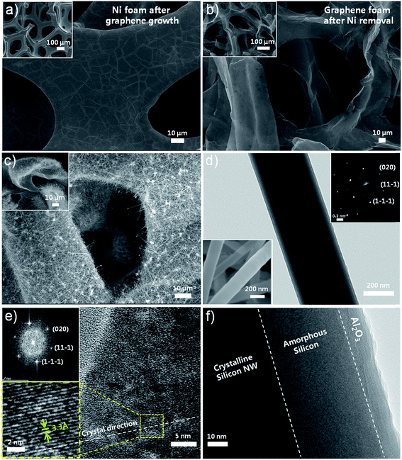
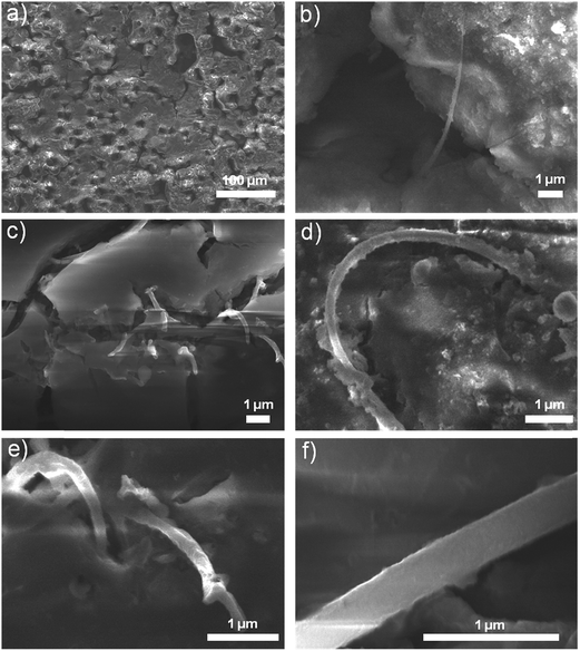
Fig. 2 shows scanning electron microscopy (SEM) and transmission electron microscopy (TEM) images of graphene layers on Ni-foam (Fig. 2a), GF after Ni removal (Fig. 2b), after SiNWs synthesis on GF (Fig. 2c), and individual SiNWs (Fig. 2d–f). Graphene layers synthesized on Ni-foam with different number of layers are continuous all over the foam (Fig. 2a), enabling us to obtain interconnected 3D-GF with a little shrinkage after the removal of supporting Ni-foam (Fig. 2b). After the SiNWs synthesis, GF is still intact, keeping the 3D foam structure, SiNWs are grown on outer surface of graphene layers and at even deep parts, thanks to large pores enabling precursors to reach in lower portions of the GF on SS during PE-CVD synthesis (Fig. 2c). Fig. 2d and f show an individual SiNW grown on GF with crystalline-Si (c-Si) core, amorphous-Si (a-Si) and 10 nm ALD coating shells. The upper inset of Fig. 2d shows selected area electron diffraction (SAED) pattern of a SiNW which is consistent with the calculated-FFT pattern in the upper inset of Fig. 2e. High resolution TEM image of an individual SiNW's crystal core is shown in Fig. 2e, representing a single-crystal structure with 3.3 Å of lattice spacing.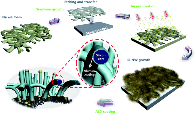 | ||
| Fig. 1 Schematic illustration of graphene foam synthesis, transfer, e-beam evaporation of Au catalyst, Si nanowire (SiNWs) growth and atomic layer deposition of alumina (ALD). | ||
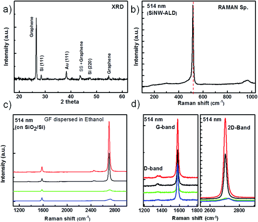
For structural analyses of GF/SiNWs composite, X-ray diffraction spectroscopy (XRD) and Raman spectroscopy were performed as shown in Fig. 3. The XRD spectrum (Fig. 3a) of GF/SiNWs composite contains 6 perfectly distinguishable peaks associated with graphene at 26.6°, 43.5° and 54.7°; with Si at 28.5° and 47.3°; and with Au (deposited as SiNW catalyst) at 38.2°, which are consistent with the literature.39,40 The graphene peak at 43.5° may also be correlated to stainless steel (SS) substrate as indicated in the Fig. 3a. Raman spectroscopy of GF/SiNWs composite (Fig. 3b) shows a clear peak at ∼517 cm−1. In the case of c-Si, first order transverse-optical (TO) phonon mode will display a sharp peak at 520 cm−1 which usually becomes broaden and is downshifted when the long-range order in Si is lost.41 In our case, a red shift of 3 cm−1 and a small broaden band at around 490 cm−1 are caused by the co-existence of c-Si and a-Si which is in good agreement of Fig. 2. Fig. 3c shows Raman spectroscopy results from graphene foam as synthesized and sonicated in ethanol solution then as coated on Si/SiO2 substrate. In some position on graphene flakes coated on Si/SiO2 substrate obtained from graphene foam shows monolayer with very high intensity ratios of 2D/G bands as well as few layers in other positions with no observable D-peaks showing the high crystallinity of graphene foams with different number of graphitic layers.
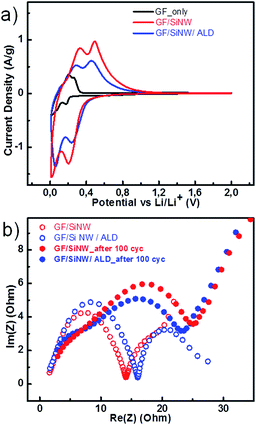
Fig. 4a shows the 2nd-cycle cyclic voltammograms (CV) of GF and GF/SiNWs composites with/without ALD coating. In the case of GF (black), charge peaks at 0.01 and 0.17 V (vs. Li/Li+) and discharge peaks at 0.2 and 0.27 V (vs. Li/Li+). The charge current associated with Li–Si alloying reaction in GF/SiNWs composite was observed at 0.01 and 0.2 V (vs. Li/Li+) in the case of as prepared samples (red). Similarly in the case of ALD coated composite (blue), lithiation peaks were observed at 0.05 and 0.24 V (vs. Li/Li+) with a slight peak-shift which might be correlated to sluggish Li–Si reaction after ALD coating. In discharge state, for the GF/SiNWs composites, two peaks around 0.3 V and 0.5 V were observed as delithiation of Li–Si alloys and correlated to the discharge plateau at 0.4 V in the voltage profile curves (Fig. 4a). These obtained results are in agreement with those for Si anodes11 and for Si/graphene composites.18,42 In the following cycles the magnitude of all current peaks were increased with cycling. Although CV profiles of ALD coated GF/SiNWs composite and uncoated one exhibit similar characteristics, the amplitude of ALD-coated sample is slightly smaller, indicating that insulating nature of alumina may affect the reaction of Si with lithium ions, decreasing overall capacity slightly, at initial cycles.
Nyquist plots GF/SiNWs composites in Fig. 4b, compares the as-prepared and ALD coated composites. Semicircle and the linear portions of the plots are indicating the electrode reactions controlled by charge transfer at high frequencies and by diffusion at low frequencies. However, in the case of ALD-coated composite (before cycling), the second semicircle indicates that ALD-coating may slow down the diffusion at low frequencies initially, while showing a better diffusion for the later cycles with alumina's well known Li-permeable structure.43 After 100 cycles of lithiation/delithiation, the charge resistance of both samples were increased, however, this increment was much smaller in the case of ALD-coated composites compared to that of as-prepared composites. This behavior can be attributed to that composite with ALD coating has better cycling stability, although they have slower charge transfer at the beginning, having a larger diameter of semi-circle before cycling. This results are in agreement with the results obtained by Wu Q. H., et al.8 and Ren J. G., et al.44 confirming the positive effect of ALD coating resulting in a stable battery performance and good electrochemical impedance characteristics.8,44
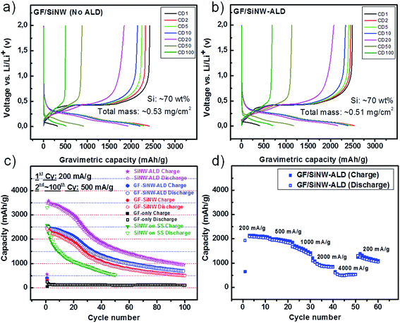
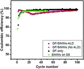
In Fig. 5a and b, the voltage profiles of GF/SiNWs composites as prepared and with ALD-coating were shown, respectively. For the first cycles at a current density of 200 mA g−1, both samples show similar gravimetric discharge capacities of 2423 and 2494 mA h g−1. However, in following cycles at current density of 500 mA g−1, as-prepared composites showed faster decay in discharge capacity compared to that of ALD coated composite. For instance at 20th cycle, ALD coated sample showed 83% capacity retention (2074 mA h g−1) while, as prepared sample retained only 76% of the first cycle. At 50th cycles, discharge capacities were decreased to 1125 mA h g−1 and 875 mA h g−1 for ALD coated and as-prepared samples, respectively. A flat plateau around 0.4 V (Li/Li+) was diminished at subsequent cycles as reported for the amorphization of Si to react with Li.11 However, by ALD-coating this delayed reduction resulted in a comparably better cycling stability. Capacity-cycling profiles of the same samples in Fig. 5a and b was also shown in Fig. 5c. For comparison, the calculated specific capacity of SiNWs from the same composite of GF/SiNW-ALD and pure SiNWs grown on SS substrate was added in Fig. 5c. This SiNWs-only capacity from the composite with ALD-coating was calculated from the following equation:45
| QSi = mGF/mSi{Qcomposite(1 + mSi/mGF) − QGF} |
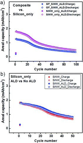
For investigating the rate capability of ALD-coated GF/SiNWs composites, different current densities of 200 mA g−1, 500 mA g−1, 1000 mA g−1, 2000 mA g−1 and 4000 mA g−1 were applied (Fig. 5d). GF/SiNWs composites with ALD-coating showed stable and reversible capacities at high rates, such as ∼850 mA h g−1 and ∼550 mA h g−1 with current densities of 2000 and 4000 mA g−1, respectively, which are comparable to report for Si/carbon material composites.46 In Fig. 7a, the areal capacities of GF/SiNWs composite and calculated capacities for only SiNWs were compared. Well-known large surface areas up to 850 m2 g−1 of GFs accommodate high mass loading of SiNWs over 0.3 mg cm−2. This unique high density Si mass loading improved the areal discharge capacities up to 1.8 mA h cm−2 for SiNWs-only and 1.3 mA h cm−2 for GF/SiNWs composite. Even after 100 cycles, discharge capacities of 0.5 mA h cm−2 for SiNWs-only and 0.35 mA h cm−2 for GF/SiNWs composite were achieved. The effect of ALD coating of alumina (ALD) for SiNWs-only can be seen in Fig. 7b. Although, at initial cycles both ALD-coated and as-prepared samples show similar values, after 50 cycles, ALD-coated sample retained 45% of its original areal discharge capacity, while as-prepared sample retained only 36% of its original areal discharge capacity. High and low magnification SEM images taken after 100 cycles of ALD-coated GF/SiNWs composite confirmed that, although SEI-layer covered all over the surface, SiNWs in the composite were still observable (Fig. 8).
Experimental
Preparation steps of GF/SiNWs composite were depicted in Fig. 1 GFs were synthesized on nickel foams (Alantum Advanced Technology Materials, China) with 420 g m−2 in areal density and 1.6 mm in thickness by atmospheric pressure CVD. Nickel foams were placed in the center of a quartz tube of atmospheric pressure CVD chamber and samples were kept under Ar (500 sccm) and H2 (200 sccm) at 1000 °C for reduction of surface oxide on Ni foams. CH4 (3 sccm) was then flowed for 5 min with same amount of Ar and H2. Following the synthesis, CH4 was turned off and the chamber was cooled down to room temperature under the same Ar and H2 ambient at a cooling rate of ≈100 °C min−1. Graphene coated Ni foams were then coated with poly(methyl methacrylate) (PMMA) solution and baked at 180 °C for 30 min followed by etching in Ni etchant (Transene Inc, TFB) at 90 °C for 5 h. After complete removal of Ni, GFs coated with PMMA were immersed into hot acetone for 30 min and transferred onto stainless steel (SS) substrates. For further details see ref. 35 and 47. For the complete removal of PMMA, samples then annealed at 600 °C in ultrahigh vacuum chamber for 2 h. For the SiNWs growth on GF, samples were then deposited ∼25 nm Au by e-beam evaporator, and placed into a plasma enhanced CVD (PECVD) chamber (A-Tech, South Korea). Samples in the chamber were heated up to 420 °C in H2 (120 sccm) ambient followed by SiH4 (30 sccm) introduction with plasma (RF power: 20 W) under pressure of 600 mTorr for 2 h. After the synthesis of SiNWs, samples were cooled down to room temperature under vacuum (10−6 Torr). Before and after GF transfer, after Si deposition, each sample was carefully weighed, using an A&D microbalance BM-22 (A&D Company Limited, Japan) with a sensitivity and precision of 1 μg. Alumina (Al2O3) coating of SiNWs on GF was performed by an ALD system (Lucida D100, NCD Technology, Korea) at 200 °C using trimethyl aluminum (TMA) and H2O as precursors. ALD film thickness was controlled by precursor pulse cycles where each cycle was fixed to 1 Å per cycle. For all samples with ALD, 100 cycles were used to obtain 10 nm of ALD coating.Scanning electron microscopy (JEOL, FESEM JSM-7600F) and high-resolution transmission electron microscopy (HR-TEM) (JEOL, JEM 2100F) were used to investigate the surface morphology and electron diffraction patterns of SiNWs. Raman spectroscopy (Renishaw, RM-1000 Invia) with excitation energy of 2.41 eV (514 nm, Ar+ ion laser) was used to characterize the optical properties of the GF and SiNWs. X-ray diffraction (XRD) ((Bruker D2 Phaser) with CuKα radiation) patterns were used to analyze the crystal structure of GF/SiNWs composite.
Electrochemical properties were evaluated by galvanostatic cycling of coin cells (CR 2032) with GF/SiNWs composite on SS substrate as the working electrode and lithium foil (99.9% purity, 0.38 mm thickness, Sigma Aldrich) as the counter/reference electrode. The mass loading was 0.5–0.55 mg cm−2 of composite with ∼70 wt% mass loadings of SiNWs. The electrolyte for all tests was 1 M LiPF6 in ethylene carbonate/diethyl carbonate (1![[thin space (1/6-em)]](https://www.rsc.org/images/entities/char_2009.gif) :
:![[thin space (1/6-em)]](https://www.rsc.org/images/entities/char_2009.gif) 1 v/v, Puriel, Techno semichem Co. Ltd, Korea) and separators from (Celgard 2500) were used. After the assembly of coin cells in dry room, all cells were kept for 24 h as wetting time of samples in electrolyte. For all measurements the total mass of GF/SiNWs composite were used. Si-only specific capacities were calculated from capacities GF-only and GF/SiNWs composite specific capacities as explained in ref. 45.
1 v/v, Puriel, Techno semichem Co. Ltd, Korea) and separators from (Celgard 2500) were used. After the assembly of coin cells in dry room, all cells were kept for 24 h as wetting time of samples in electrolyte. For all measurements the total mass of GF/SiNWs composite were used. Si-only specific capacities were calculated from capacities GF-only and GF/SiNWs composite specific capacities as explained in ref. 45.
Conclusions
A facile direct fabrication route to the synthesis of SiNWs on a highly conductive porous 3D graphene network of GFs, with improved Si-mass loadings have been demonstrated. GF underneath the SiNWs utilized as a conductive and a flexible support to enhance the gravimetric and areal capacities at reasonable current densities. Furthermore, GF's excellent elastic property improved the stress induced pulverization of SiNWs, resulting in a better cycling performance of GF/SiNWs composite, though cycling performance still need to be improved. ALD coating of composite further comparably improved the cycle life. We believe this direct Si and 3D-graphene hybrid fabrication method can open up new possibilities for more advanced anode materials in Li-ion batteries.Acknowledgements
Special thanks to Prof. Young Hee Lee of Center for Integrated Nanostructure Physics IBS, Sungkyunkwan University for his valuable discussions and supports.References
- L. Hu, H. Wu, Y. Gao, A. Cao, H. Li, J. McDough, X. Xie, M. Zhou and Y. Cui, Adv. Energy Mater., 2011, 1, 523–527 CrossRef CAS.
- S. W. Lee, B. M. Gallant, H. R. Byon, P. T. Hammond and Y. Shao-Horn, Energy Environ. Sci., 2011, 4, 1972–1985 CAS.
- N. Du, H. Zhang, J. Yu, P. Wu, C. Zhai, Y. Xu, J. Wang and D. Yang, Chem. Mater., 2009, 21, 5264–5271 CrossRef CAS.
- Y. Qi, N. Du, H. Zhang, X. Fan, Y. Yang and D. Yang, Nanoscale, 2012, 4, 991–996 RSC.
- J. Chmiola, C. Largeot, P.-L. Taberna, P. Simon and Y. Gogotsi, Science, 2010, 328, 480–483 CrossRef CAS PubMed.
- Z. Guo, X. Dong, D. Zhou, Y. Du, Y. Wang and Y. Xia, RSC Adv., 2013, 3, 3352–3358 RSC.
- L. Qiu, Z. Shao, W. Wang, F. Wang, D. Wang, Z. Zhou, P. Xiang and C. Xu, RSC Adv., 2014, 4, 24859–24862 RSC.
- Q.-H. Wu, B. Qu, J. Tang, C. Wang, D. Wang, Y. Li and J.-G. Ren, Electrochim. Acta, 2015, 156, 147–153 CrossRef CAS.
- A. M. Chockla, J. T. Harris, V. A. Akhavan, T. D. Bogart, V. C. Holmberg, C. Steinhagen, C. B. Mullins, K. J. Stevenson and B. A. Korgel, J. Am. Chem. Soc., 2011, 133, 20914–20921 CrossRef CAS PubMed.
- S. Jeong, J.-P. Lee, M. Ko, G. Kim, S. Park and J. Cho, Nano Lett., 2013, 13, 3403–3407 CrossRef CAS PubMed.
- C. K. Chan, H. Peng, G. Liu, K. McIlwrath, X. F. Zhang, R. A. Huggins and Y. Cui, Nat. Nanotechnol., 2008, 3, 31–35 CrossRef CAS PubMed.
- T. Hatchard and J. Dahn, J. Electrochem. Soc., 2004, 151, A838–A842 CrossRef CAS.
- X. Wang, Z. Li, J. Shi and Y. Yu, Chem. Rev., 2014, 114, 9346–9384 CrossRef CAS PubMed.
- S. Jing, H. Jiang, Y. Hu and C. Li, Nanoscale, 2014, 6, 14441–14445 RSC.
- W. Xu and J. C. Flake, J. Electrochem. Soc., 2010, 157, A41–A45 CrossRef CAS.
- W. Wang, M. K. Datta and P. N. Kumta, J. Mater. Chem., 2007, 17, 3229–3237 RSC.
- Z. Wen, J. Yang, B. Wang, K. Wang and Y. Liu, Electrochem. Commun., 2003, 5, 165–168 CrossRef CAS.
- X. Xin, X. Zhou, F. Wang, X. Yao, X. Xu, Y. Zhu and Z. Liu, J. Mater. Chem., 2012, 22, 7724–7730 RSC.
- J. K. Lee, K. B. Smith, C. M. Hayner and H. H. Kung, Chem. Commun., 2010, 46, 2025–2027 RSC.
- X. Gao, J. Li, Y. Xie, D. Guan and C. Yuan, ACS Appl. Mater. Interfaces, 2015, 7, 7855–7862 CAS.
- Y. Yang, G. Yu, J. J. Cha, H. Wu, M. Vosgueritchian, Y. Yao, Z. Bao and Y. Cui, ACS Nano, 2011, 5, 9187–9193 CrossRef CAS PubMed.
- B. Wang, X. Li, T. Qiu, B. Luo, J. Ning, J. Li, X. Zhang, M. Liang and L. Zhi, Nano Lett., 2013, 13, 5578–5584 CrossRef CAS PubMed.
- M. Winter, J. O. Besenhard, M. E. Spahr and P. Novak, Adv. Mater., 1998, 10, 725–763 CrossRef CAS.
- I. Lahiri, S.-W. Oh, J. Y. Hwang, S. Cho, Y.-K. Sun, R. Banerjee and W. Choi, ACS Nano, 2010, 4, 3440–3446 CrossRef CAS PubMed.
- X.-M. Liu, Z. Dong Huang, S. Woon Oh, B. Zhang, P.-C. Ma, M. M. Yuen and J.-K. Kim, Compos. Sci. Technol., 2012, 72, 121–144 CrossRef CAS.
- D. Chattopadhyay, I. Galeska and F. Papadimitrakopoulos, J. Am. Chem. Soc., 2003, 125, 3370–3375 CrossRef CAS PubMed.
- B. J. Landi, H. J. Ruf, C. M. Evans, C. D. Cress and R. P. Raffaelle, J. Phys. Chem. B, 2005, 109, 9952–9965 CrossRef CAS PubMed.
- H. Liu, K. Cao, X. Xu, L. Jiao, Y. Wang and H. Yuan, ACS Appl. Mater. Interfaces, 2015, 7, 11239–11245 CAS.
- H. Xiang, K. Zhang, G. Ji, J. Y. Lee, C. Zou, X. Chen and J. Wu, Carbon, 2011, 49, 1787–1796 CrossRef CAS.
- J. Luo, X. Zhao, J. Wu, H. D. Jang, H. H. Kung and J. Huang, J. Phys. Chem. Lett., 2012, 3, 1824–1829 CrossRef CAS PubMed.
- X. Zhou, A.-M. Cao, L.-J. Wan and Y.-G. Guo, Nano Res., 2012, 5, 845–853 CrossRef CAS.
- C. Wang, Y.-S. Chui, R. Ma, T. Wong, J.-G. Ren, Q.-H. Wu, X. Chen and W. Zhang, J. Mater. Chem. A, 2013, 1, 10092–10098 CAS.
- J.-G. Ren, C. Wang, Q.-H. Wu, X. Liu, Y. Yang, L. He and W. Zhang, Nanoscale, 2014, 6, 3353–3360 RSC.
- F. Yao, F. Güneş, H. Q. Ta, S. M. Lee, S. J. Chae, K. Y. Sheem, C. S. Cojocaru, S. S. Xie and Y. H. Lee, J. Am. Chem. Soc., 2012, 134, 8646–8654 CrossRef CAS PubMed.
- Z. Chen, W. Ren, L. Gao, B. Liu, S. Pei and H.-M. Cheng, Nat. Mater., 2011, 10, 424–428 CrossRef CAS PubMed.
- H. Sahin, O. Leenaerts, S. Singh and F. Peeters, arXiv preprint arXiv:1502.05804, 2015.
- M. N. Nair, Functionalization of epitaxial graphene by metal intercalation and molecules, Université de Haute Alsace-Mulhouse, 2013 Search PubMed.
- C. Wang, Y. Li, Y.-S. Chui, Q.-H. Wu, X. Chen and W. Zhang, Nanoscale, 2013, 5, 10599–10604 RSC.
- C. Peng, H. Chen, Q. Li, W. Cai, Q. Yao, Q. Wu, J. Yang and Y. Yang, J. Mater. Chem. A, 2014, 2, 13859–13867 CAS.
- T. Mondal, A. K. Bhowmick and R. Krishnamoorti, J. Mater. Chem., 2012, 22, 22481–22487 RSC.
- M. Holzapfel, H. Buqa, L. J. Hardwick, M. Hahn, A. Würsig, W. Scheifele, P. Novák, R. Kötz, C. Veit and F.-M. Petrat, Electrochim. Acta, 2006, 52, 973–978 CrossRef CAS.
- X. Zhou, Y.-X. Yin, L.-J. Wan and Y.-G. Guo, Chem. Commun., 2012, 48, 2198–2200 RSC.
- B. Li, F. Yao, J. J. Bae, J. Chang, M. R. Zamfir, D. T. Le, D. T. Pham, H. Yue and Y. H. Lee, Sci. Rep., 2015, 5, 7659 CrossRef CAS PubMed.
- J. G. Ren, Q. H. Wu, G. Hong, W. J. Zhang, H. Wu, K. Amine, J. Yang and S. T. Lee, Energy Technol., 2013, 1, 77–84 CrossRef CAS.
- A. Ghosh and Y. H. Lee, ChemSusChem, 2012, 5, 480–499 CrossRef CAS PubMed.
- X. Li, J. H. Cho, N. Li, Y. Zhang, D. Williams, S. A. Dayeh and S. Picraux, Adv. Energy Mater., 2012, 2, 87–93 CrossRef CAS.
- H. Y. Yue, S. Huang, J. Chang, C. Heo, F. Yao, S. Adhikari, F. Gunes, L. C. Liu, T. H. Lee and E. S. Oh, ACS Nano, 2014, 8, 1639–1646 CrossRef CAS PubMed.
| This journal is © The Royal Society of Chemistry 2016 |

