
Two-dimensional layered nanomaterials for gas-sensing applications
Wei
Yang
,
Lin
Gan
*,
Huiqiao
Li
and
Tianyou
Zhai
*
State Key Laboratory of Material Processing and Die & Mould Technology, School of Materials Science and Engineering, Huazhong University of Science and Technology (HUST), Wuhan 430074, P. R. China. E-mail: zhaity@hust.edu.cn; ganlinust@hust.edu.cn
First published on 13th January 2016
Abstract
Owing to the unique thickness dependent physical and chemical properties, two-dimensional (2D) layered nanomaterials have received tremendous attention and shown great potential in the fabrication of high-performance electronic/optoelectronic devices. Notably, the implication of 2D nanomaterials in the gas-sensing field has also drawn considerable attention but few related review studies have been reported. This critical review mainly focuses on the current progress of 2D layered nanomaterials in gas-sensing applications. Firstly, we describe the basic attributes of 2D layered nanostructures and discuss the fundamentals of their gas-sensing applications. Secondly, we have numerated recent gas-sensing studies on typical 2D layered nanomaterials, including graphene, MoS2, MoSe2, WS2, SnS2, black phosphorus, and others. Particularly, the optimized strategies for improving their gas-sensing performances are also discussed here. Finally, we conclude this review with some perspectives and the outlook on future advances in this field.
 Tianyou Zhai | Tianyou Zhai received his B.S. degree in chemistry from Zhengzhou University in 2003, and then received his Ph.D. degree in physical chemistry from the Institute of Chemistry, Chinese Academy of Sciences (ICCAS) under the supervision of Prof. Jiannian Yao in 2008. Afterwards he joined the National Institute for Materials Science (NIMS) as a JSPS postdoctoral fellow of Prof. Yoshio Bando's group and then as an ICYS-MANA researcher within NIMS. Currently, he is a Chief Professor of the School of Materials Science and Engineering, Huazhong University of Science and Technology (HUST). His research interests include the controlled synthesis and exploration of fundamental physical properties of inorganic functional nanomaterials, as well as their promising applications in energy science, electronics and optoelectronics. He has authored and co-authored above 100 peer-reviewed journal articles, 5 book chapters, co-edited 1 book on nanotechnology, and held 7 patents. His publications have been cited more than 5100 times (H-index is 41). |
1. Introduction
Gas sensors that identify the presence and/or concentration of a specific gas in ambient atmosphere have attracted enormous attention and have found applications in many fields, such as environmental monitoring, process control, security, medical diagnostics, etc.1,2 Among various types of gas sensors, metal oxide-based gas sensors have been extensively investigated in the past few decades due to their relatively low cost and high sensitivities.3–5 However, to obtain a high response to targeted gases, a relatively high operating temperature would generally be adopted, which not only increases the power consumption but also causes thermal safety problems, thus hindering their practical applications. Therefore, novel sensors which can work effectively at low temperature, especially at room temperature, are highly desired. Several strategies, such as exploiting novel gas-sensing materials, optimizing device geometry, and adopting suitable fabrication techniques, have been developed to address this issue. Notably, all these methods are strongly dependent on the characteristics of the gas-sensing materials. Thus, developing novel gas-sensing materials with ultrahigh surface-to-volume ratios and strong surface activities is a strikingly primary and reliable approach for fabricating gas sensors operated at a low or room temperature. Since these samples possess an ultra-large specific surface area and high surface activities, the interaction of gas molecules with the surfaces is very strong which ultimately improves the sensitivity and kinetics of sensing.Two-dimensional (2D) layered nanomaterials have aroused huge interest due to their excellent semiconducting performances and unique thickness dependent physical and chemical properties, including ultra-large surface-to-volume ratios, high surface activities, etc.6–10 Furthermore, 2D layered nanomaterials can be easily fabricated as chemiresistive field effect transistors (FETs) that have low power consumption and good safety. Such advantages of 2D layered nanomaterials distinguish them from conventional metal oxides, and render them a promising future in the development of ultrahigh sensitive and low-power-consumption sensor platforms. Up to now, some intrinsic 2D nanomaterials with layered characteristics, such as graphene,11–13 metal dichalcogenides (e.g. MoS2,14–20 MoSe2,21 WS2,22–24 SnS2,25,26 and VS2![[thin space (1/6-em)]](https://www.rsc.org/images/entities/char_2009.gif) 27), black phosphorus (BP),28–31 hexagonal boron nitride (h-BN)32 and graphitic carbon nitride (g-C3N4),33 have been developed as gas-sensing materials and opened up new avenues for fabricating low or room temperature gas sensors. In addition, there are many studies on the preparation of hybrid 2D functional materials in which many materials are incorporated into the 2D system for gas-sensing applications, such as layer-by-layer assembly34–36 and the Langmuir–Blodgett (LB) method.37–39 These strategies have been elaborated in other studies,40,41 thus herein we focus mainly on these inherent 2D layered nanomaterials for gas-sensing applications. Recent reviews have described the synthesis, properties, and potential applications of intrinsic 2D nanomaterials in various aspects, including electronic devices, optoelectronic devices, energy storage devices, as well as sensing platforms.42–47 However, there are few review studies systematically focused on their gas-sensing applications until now, thus it is necessary to make a full summary on such a topic.
27), black phosphorus (BP),28–31 hexagonal boron nitride (h-BN)32 and graphitic carbon nitride (g-C3N4),33 have been developed as gas-sensing materials and opened up new avenues for fabricating low or room temperature gas sensors. In addition, there are many studies on the preparation of hybrid 2D functional materials in which many materials are incorporated into the 2D system for gas-sensing applications, such as layer-by-layer assembly34–36 and the Langmuir–Blodgett (LB) method.37–39 These strategies have been elaborated in other studies,40,41 thus herein we focus mainly on these inherent 2D layered nanomaterials for gas-sensing applications. Recent reviews have described the synthesis, properties, and potential applications of intrinsic 2D nanomaterials in various aspects, including electronic devices, optoelectronic devices, energy storage devices, as well as sensing platforms.42–47 However, there are few review studies systematically focused on their gas-sensing applications until now, thus it is necessary to make a full summary on such a topic.
In this critical review, we mainly focus on the current developments of gas sensors based on some kinds of typical 2D layered nanomaterials, including graphene, MoS2, MoSe2, WS2, SnS2, VS2, BP, BN, and C3N4. Moreover, the optimized approaches for enhancing their gas-sensing behaviours are also discussed here. Finally, we conclude this article with some perspectives and outlooks on this new trend in the gas sensing field.
2. Fundamentals of gas-sensing on 2D layered nanomaterials
2.1 Gas-sensing mechanism for 2D layered nanomaterials
Development of gas sensors based on intrinsic 2D layered nanomaterials is strictly dependent on their sensing mechanism. Unlike typical metal oxides (e.g., SnO2, ZnO, In2O3), the sensing mechanism of typical 2D layered nanomaterials (especially graphene, MoS2, and WS2) is based on a charge transfer process.18,19,48 When the sensors are exposed to reactive gas, the gas species are adsorbed on the surfaces of sensing channels, leading to the variation of sensor resistance. Upon exposure to air or an inert environment, in contrast, the gas molecules are desorbed from the sensing materials, and the sensor resistances go back to their original state. In detail, taking CVD-grown monolayer MoS2 (n-type semiconductor) as a typical example, the charge transfer processes between gaseous species (e.g., NO2, NH3) and sensing devices can serve as a rational sensing mechanism discussed in the following.19 When NO2 molecules are adsorbed onto MoS2 surfaces, an unpaired electron from the nitrogen atom in NO2 usually acts as a strong oxidizer (electron acceptor), and tends to withdraw electrons from the MoS2 surface (Fig. 1a). As a result, a decreased electron concentration in the conduction band of the MoS2 occurs. Such a charge transfer induces a decreased carrier concentration and thus degraded electrical conductivity. In contrast, NH3 having a lone electron pair always serves as an electron donor, and transfers its electrons to the conduction band of MoS2, thus this will lead to an increased electron concentration and electrical conductivity in MoS2 (Fig. 1b). The charge transfer processes between the adsorbed gaseous species and MoS2 are verified by an in situ photoluminescence (PL) study. When the sensor was exposed to oxidative NO2, the intensity of the quasi-particle (A+) peak in the PL spectrum increased, whereas the neutral exciton (A0) peak decreased (Fig. 1c). This is attributed to the extraction of electrons from the MoS2 by NO2 and the generation of the corresponding holes in MoS2. In contrast, an opposite trend was observed for NH3 gas because of dissociation of the positive trions from the neutral excitons, leading to a suppressed intensity of the A+ peak and increased A0 (Fig. 1d).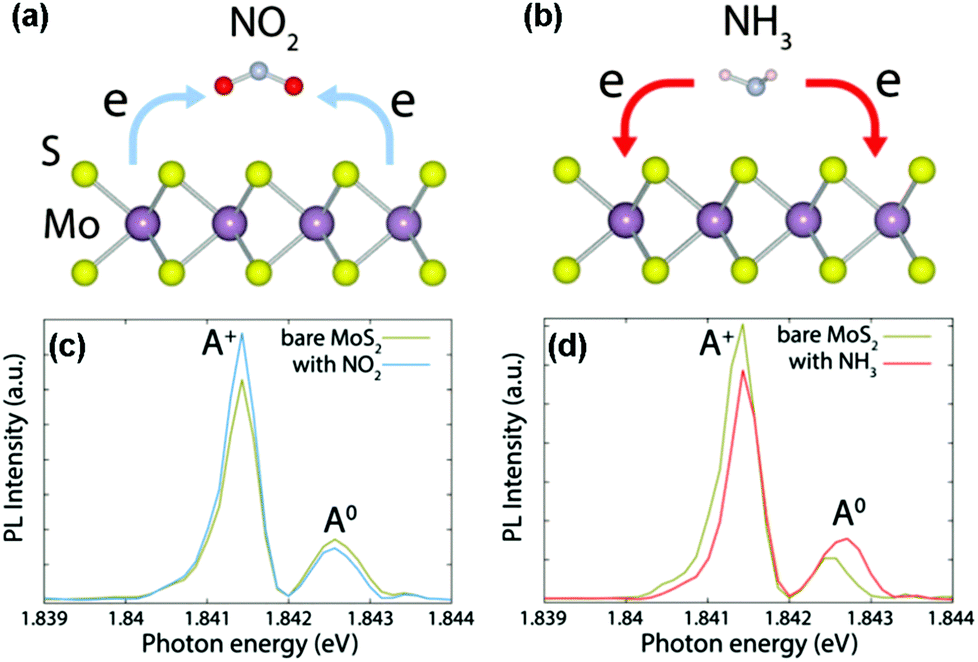 | ||
| Fig. 1 Schematics of the charge transfer processes for MoS2 in the presence of NO2 (a) and NH3 (b) molecules. In situ PL spectra recorded from MoS2 with NO2 (c) and NH3 (d) molecules (reproduced from ref. 19). | ||
2.2 Configurations of gas-sensing devices
The chemiresistor-type gas-sensing device is widely applied in which the resistance of the sensing material changes under exposure to the targeted gas. This type of sensing device has several advantages, such as a simple fabrication process, direct measurement and easy operation.49–51Fig. 2a exhibits a typical structure of a chemiresistive gas sensor. The dispersed solution containing sensing materials was dropped onto a ceramic plate which was previously coated with a pair of gold electrodes deposited by the screen printing technique. A RuO2 heater was mounted on the reverse sides of the ceramic plate to control the sensing temperature. This type of sensing device has been applied to various kinds of gas species, including NO2, NH3, H2S, H2, ethanol and formaldehyde.52–54 | ||
| Fig. 2 Two typical configurations of gas-sensing devices: (a) chemiresistor (reproduced from ref. 52); (b) field effect transistor (FET) (reproduced from ref. 18). | ||
The field effect transistor (FET) is another important type of electronic gas sensor and has been demonstrated to be a competitive configuration for 2D layered nanomaterial-based sensors.55 In this case, the drain current (Ids) of a FET-based sensor depends on the gate bias (Vg), and it can be effectively tuned upon the exposure of gas species. The sensing performance of FET-based devices is mainly evaluated by the on/off current ratios. A high sensitivity usually accompanies a high on/off current ratio.56 Up to now, there are many functional nanostructures, especially 2D layered nanomaterials, suitable as channel materials for FET type gas sensors due to their excellent semiconducting properties and large lateral size.18,57,58Fig. 2b presents the structure of a MoS2-based FET sensor and it has been applied for the detection of NO2 and NH3.18 When the sensor was exposed to reactive molecules (NO2, NH3), these molecules were adsorbed onto the surfaces of the sensing materials, leading to a change of the local charge carrier concentration, and this signal could be monitored sensitively as current altering.
The surface acoustic wave (SAW) technique has also been developed for the detection of a variety of gas species, such as CO, H2, methanol, chloroform.59,60 This type of sensor is based on the frequency changes caused by the conductance or mass change of their sensing layers by exposure to gas molecules. As a typical example, Kaner et al.59 reported a SAW graphene sensor for the detection of H2 and CO. The sensor responses were approximately 5.8 kHz to 1% H2 and 8.5 kHz to 1000 ppm CO at room temperature, respectively. Notably, the molecular weight of CO is 14 times heavier than that of H2. Thus, the dominant factor for CO sensing was the mass change, while the H2 sensing was mainly attributed to the conductance change of graphene nanosheets. In another example, Balandin et al.60 demonstrated a SAW sensor for distinguishing various chemical vapours. The characteristic frequency (fc) of the Lorentzian noise bulges in the sensor is distinct for different vapors with variations from fc = 10–20 Hz to fc = 1300–1600 Hz for tetrahydrofuran and chloroform vapours, respectively.
3. Gas sensors based on 2D layered nanomaterials
3.1 Graphene-based gas sensors
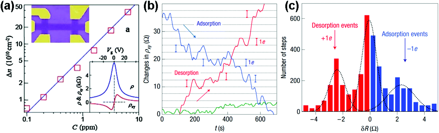 | ||
| Fig. 3 (a) Concentration variation (Δn) of charge carriers in single-layer graphene exposed to different NO2 concentrations (C). Upper inset: scanning electron micrograph of this device. Lower inset: characterization of the graphene device by using the electric-field effect. (b) The changes of Hall resistivity (ρxy) observed near the neutrality point during adsorption (blue curve) and desorption (red curve) of strongly diluted NO2. The green curve presents a reference exposed to pure He. (c) For analysis, all changes in ρxy were recorded larger than 0.5 Ω and quicker than 10 s as individual steps (reproduced from ref. 64). | ||
Inspired by the work described above, many efforts have been made to exploit the gas-sensing performances of pristine graphene prepared by the mechanically exfoliated method. For instance, Balandin et al.60 demonstrated a exfoliated graphene based transistor that can selectively detect different organic vapours. Fig. 4a exhibited the SEM image of the back-gated graphene transistor using the electron beam lithography (EBL) technique. The noise frequency characteristics induced by different chemical vapours are also shown in Fig. 4b. The characteristic frequencies of these bulges are clearly variable for different gas chemicals. Moreover, the noise frequency range and the relative resistance changes can serve as distinctive signals for specific gases, rendering the graphene device with a highly selective gas-sensing attribute.
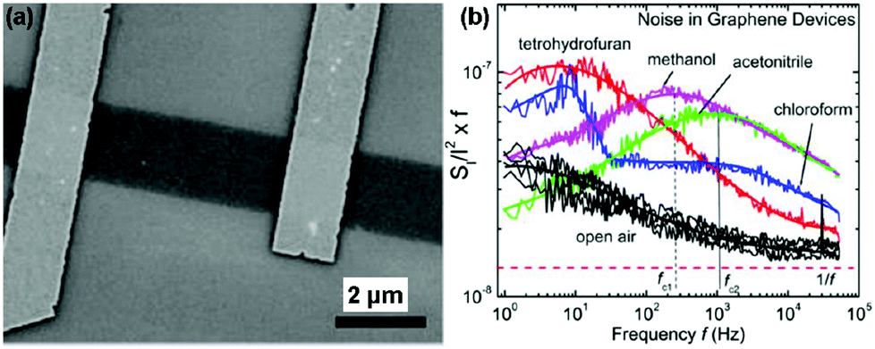 | ||
| Fig. 4 (a) SEM images of back-gated graphene devices. (b) Noise spectral density (SI/I2) multiplied by frequency (f) versus f for the device in the presence of open air and different vapours (reproduced from ref. 60). | ||
Although high-quality graphene can be prepared by the mechanical exfoliation method, the size of most graphene films is usually limited below 1000 μm2, which is not considered as a scalable technique.67 Large-area synthesis of high-quality pristine graphene sheets can be achieved by the chemical vapour deposition (CVD) method. In the CVD synthesis, metal substrates such as copper, nickel and cobalt, were applied to catalytically decompose the hydrocarbons at moderate temperatures (<1000 °C).68–73 The deposited graphene sheets could be transferred to arbitrary substrates (rigid or flexible) for the fabrication of gas sensing devices.74–76 As a typical example, very recently, Jang et al.68 presented a self-activated transparent gas sensor based on CVD-grown graphene with endurance to humidity and mechanical bending. Fig. 5a showed the fabrication procedure of a graphene sensor. Firstly, the graphene layer was grown and directly patterned on a Cu foil. Subsequently, poly(methyl methacrylate) (PMMA) was coated on top of the patterned graphene to transfer the sample to a target substrate. Finally, the Cu foil was etched by using FeCl3 solution, and the patterned graphene with PMMA was transferred onto a polyimide (PI) substrate. The PMMA can be removed by acetone and heat treatment. When exposed to three consecutive pulses of 5 ppm NO2, the as-fabricated devices exhibited improved response and recovery with increasing bias voltage (Fig. 5b). Moreover, the dynamic sensing transients of the patterned graphene sensor to 5 ppm of NO2 in dry (0% RH) and humid (50% RH) atmospheres were also presented in Fig. 5c, indicating the negligible influence of humidity on this self-activated sensor. In addition, the sensor displayed a reliable operation under mechanical bending due to the excellent flexibility of graphene (Fig. 5d). These remarkable sensor performances significantly extended the potential applications of the all-graphene sensors in the internet of things and wearable electronics. Recently, Kumar et al.76 demonstrated for the first time a simple, low-cost chemical sensing platform based on graphene-paper (G-paper) prepared by direct transfer of CVD-grown graphene onto paper without any intermediate layers. These sensors achieved a remarkable limit of detection (LOD) of 300 ppt for NO2, which is better than those from other paper-based sensors. Moreover, G-paper sensors were also found to be robust against minor strain, which was expected to enable a flexible and portable gas-sensing platform.
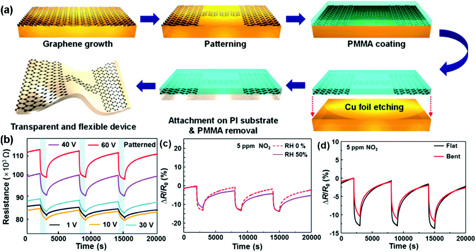 | ||
| Fig. 5 (a) Fabrication procedure of an all-graphene sensor. Response curves of the patterned graphene sensors to three pulses of 5 ppm NO2 (b) under the increased bias voltage; (c) under 0% and 50% relative humidity conditions at 60 V; (d) without and with the bending strain (reproduced from ref. 68). | ||
Large-area uniform pristine graphene films can also be achieved by the epitaxial growth method. The SiC substrate was usually applied to produce graphene layers by heating under ultrahigh vacuum, and the graphene layer thickness can be adjusted by controlling the annealing temperature and duration.77 The grown graphene layers on the SiC substrate can be directly fabricated into the sensing device without a transfer process.78 Moreover, the sensing performances of graphene-based devices were strongly influenced by the chosen substrate.79–82 For example, Nomani et al.81 reported that epitaxial-grown graphene layers on the Si- and C-faces of the semiconducting 6H-SiC displayed opposite conductance variations when exposed to NO2 molecules. The graphene layer grown on Si- and C-faces exhibited 10% decrease and 4.5% increase in conductance toward 18 ppm of NO2, respectively. The phenomenon was attributed to the different doped states of both graphene materials. In this case, the graphene films grown on the Si-face were p-type, whereas those grown on the C-face were n-type. Interestingly, an opposite direction of signal change was also observed for the epitaxially grown graphene-based sensor to various concentrations of NO2, demonstrated by Pearce et al.82 The single layer graphene on the SiC substrate exhibited n-type behaviour upon exposure to low NO2 concentration, whereas a p-type response toward high NO2 concentrations. Such results demonstrated that the single layer graphene device underwent an n–p transition when exposed to increased NO2 concentration, resulting from the tuned electronic properties of graphene induced by the SiC substrate which can act as the electron donor.
 | ||
| Fig. 6 (a) Optical image of the GO film device. (b) Plot of the normalized conductance response to 5 s pulses of acetone for GO devices reduced with hydrazine for 3, 6, 18, and 24 h. (c) Noise density spectra for SWNT and rGO devices (reproduced from ref. 97). (d) Inkjet-printed graphene oxide film lifts off the PET surface. Inset: digital image of an inkjet-printed RGO/PET four-probe sensor. Plot for resistance versus time when the film was exposed to NO2 (e) and Cl2 (f) (reproduced from ref. 100). | ||
In addition, during the chemical reduction of GO, many foreign groups or atoms are introduced to intrinsically change the surface properties of rGO, leading to the enhanced sensing performances.48,103,104 In a typical example, Shi et al.48 used chemiresistor-type NO2 sensors based on sulfonated rGO (S-G). The thickness of the S-G sheets was measured to be 0.9 to 1.1 nm by atomic force microscopy (AFM) in Fig. 7a, indicating a monolayer for the S-G. Moreover, the as-fabricated S-G sensor displayed a reversible response and recovery characteristic upon exposure to various concentrations of NO2 without the assistance of UV/IR light illumination or thermal treatment (Fig. 7b). In addition, the sensor response was about 16.4 times that of the rGO counterpart toward 50 ppm NO2. These results indicated that the chemical modification of sulfonic acid greatly improved the performance of rGO in the NO2-sensing application. Furthermore, the sensitivity of the S-G sensor was also strongly influenced by the thickness of the sensing layer. Fig. 7c showed the responses of the S-G sensors with various thicknesses of sensing layers exposed to 50 ppm NO2. The response of sensor 3 with sensing layer thickness (T) around 1–6 nm is 4.8 and 2.3 times those of sensor 1 (T = 50 nm) and sensor 2 (T = 10 nm), respectively. This is because the thinner S-G layer possessed a larger surface-to-volume ratio which is favourable for the surface adsorption of NO2. To further improve the response-recovery characteristic of the S-G device for NO2 sensing at room temperature, Huang et al.103 demonstrated a flexible chemiresistor-type sensor based on Ag nanoparticles decorated S-RGO (Ag-S-RGO), which was printed onto a polyimide (PI) substrate using a gravure printing technique. The FESEM image in Fig. 7d showed that large amounts of Ag NPs are uniformly assembled on the S-RGO surfaces and the Ag-S-RGO sheets have a few wrinkles. Moreover, the printed Ag-S-RGO sensor exhibited a fast response-recovery rate toward NO2 with a concentration range of 0.5 to 50 ppm at room temperature (Fig. 7e). When exposed to 50 ppm NO2 at room temperature, the response and recovery time of the sensor was only 12 s and 20 s, respectively. Furthermore, the Ag-S-G sensor showed almost constant resistance after 1000 bending cycles (Fig. 7f), indicating potential application in a flexible sensing device.
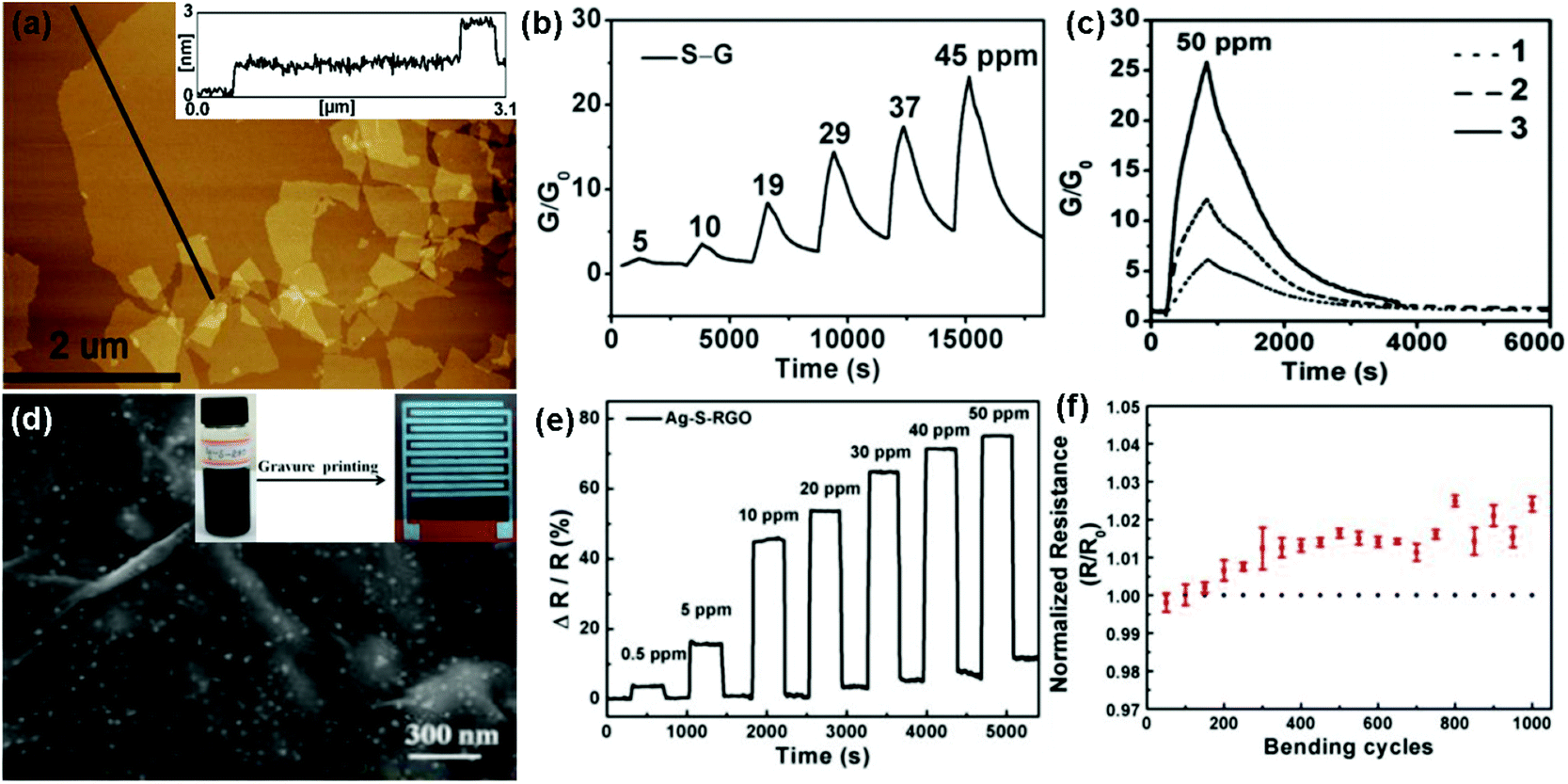 | ||
| Fig. 7 (a) AFM images of S–G sheets deposited on the mica surface. (b) Response variation of the S–G-based sensor as a function of NO2 concentrations ranging from 5 to 45 ppm. (c) Responses of the S–G-based sensors with different thicknesses of sensing layers after exposure to 50 ppm NO2: 50 nm (1), 10 nm (2), and a few layers (1–6 nm) (3) (reproduced from ref. 48). (d) FESEM image of Ag-S-RGO. Inset: photographs of Ag-S-RGO ink and Ag-S-RGO sensing layer printed onto the PI substrate with Ag interdigitated electrodes, respectively. (e) Response of the Ag-S-RGO sensor upon exposure to various NO2 concentrations. (f) Changes of the normalized resistance during the bend test for the Ag-S-RGO sensor (reproduced from ref. 103). | ||
Metals, especially noble metals (e.g., Au, Pt, Pd, and Ag) decorated graphene hybrid composites are considered as a new type of sensing material with high sensitivity and selectivity beyond conventional graphene-based materials due to their specific catalysis effect for gas-sensing. For example, Ramaprabhu et al.105 fabricated a hydrogen sensor based on Pt nanoparticle (Pt NP) decorated graphene nanosheets by a simple drop casting technique. The sensor based on the Pt NP/graphene composite exhibited a higher response (Rg/Ra − 1 = 16%) to 4 vol% H2 than that of the Pt NP decorated multi-walled carbon nanotubes (Rg/Ra − 1 = 8%) at room temperature. In another case, Liu et al.106 developed a highly sensitive NO sensing device. The device comprised sensing channels with palladium-decorated reduced graphene oxide (Pd-RGO) and the electrodes covered with chemical vapour deposition (CVD)-grown graphene were fabricated by the alternating current dielectrophoresis technique, and the detailed fabrication process is shown in Fig. 8a. The SEM image of the device (device A, graphene-Pd-RGO) is also shown in Fig. 8b. After a moderate current annealing, the novel device displayed a recoverable response upon exposure to NO ranging from 2 to 420 ppb at room temperature (Fig. 8c). To totally investigate the effects of Pd decoration of RGO, electrodes covered with CVD-grown graphene, and current annealing on sensing properties, the typical comparison results of devices A, B, C, and D upon exposure to continuously increasing NO gas concentrations (2, 24, 156, and 420 ppb) are depicted in Fig. 8d. This result demonstrated that the improved NO response of the graphene-Pd-RGO sensor can be attributed to the Pd decoration and CVD-grown graphene contacts of RGO. Functional Ag nanostructures were also employed to enhance the sensing properties of the rGO materials. Cuong et al.109 reported NH3 sensors based on Ag nanomaterial (Ag nanoparticles, Ag nanowires) coated rGO nanosheets fabricated with solution processes. When exposed to 100 ppm NH3 at room temperature, the rGO/AgNW sensor exhibited a higher sensitivity, and an excellent response and recovery characteristic compared with rGO/AgNPs, and rGO sensors. Furthermore, the effect of AgNW spray volume on the rGO/AgNW device response indicated that an excess amount of AgNWs was unfavourable for enhancing the sensing performance due to the agglomeration of the AgNWs.
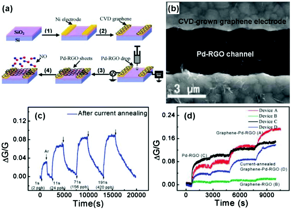 | ||
| Fig. 8 (a) Schematics of the fabrication process for the graphene-Pd-RGO device. (b) SEM image of Pd-RGO nanosheets trapped between two graphene-covered electrodes. (c) Device response exposed to 2, 24, 156, and 420 ppb NO after current annealing. (d) Responses of the various devices versus time, and the step-shaped response corresponding to 1, 10, 60, and 120 s pulses of NO: 2, 22, 132, and 264 ppb, respectively (reproduced from ref. 106). | ||
Semiconducting metal oxides, including SnO2, ZnO, In2O3, TiO2, WO3, Fe2O3, CuO and Cu2O, have been developed for fabrication of gas-sensing devices in many reports.123–126 However, the low conductivity at room temperature and high operating temperature limited their potential applications in room-temperature sensing devices. Blending metal oxides with graphene sheets to form hybrid architectures can maintain improved sensing behaviour compared with individual metal oxides and graphene.112,114,127,128 As a typical example, Chen et al.112 developed a novel and selective gas-sensing platform using SnO2 nanocrystal (SnO2 NC) decorated rGO (SnO2-rGO), as schematically depicted in Fig. 9a. The hybrid nanostructures consisting of rGO nanosheets and SnO2 NCs worked as the sensing channel in the sensor (Fig. 9b). When the sensing device was exposed to the targeted gases (e.g., NO2, NH3), the electron transfer between gas molecules and rGO occurred, thereby varying the device conductivity. Moreover, this SnO2-rGO device showed improved NO2 sensing, whereas it showed weakened NH3 sensing compared with the bare rGO (Fig. 9c and d). The reported findings implied a promising direction for tuning the sensitivity and selectivity of the rGO-based sensor. Similarly, Sow et al.114 prepared the octahedral Cu2O nanowire mesocrystal coupled rGO composite (Cu2O/rGO) under hydrothermal conditions and developed their applications in the detection of NO2. When exposed to NO2 with a concentration range of 0.4–2 ppm at room temperature, the sensor based on the Cu2O/rGO hybrid composite exhibited a higher response than that of rGO and Cu2O alone. The theoretically calculated LODs for the composite-, rGO- and Cu2O-based sensors were 64 ppb, 81 ppb and 82 ppb, respectively. The enhanced gas-sensing performance of the Cu2O/rGO composite can be mainly attributed to its high specific surface area and improved conductivity, induced by the highly oriented and porous interpenetrating structured Cu2O nanowire mesocrystals coupled on the rGO nanosheets. In addition, metal oxide quantum dot (QD) decorated rGO hybrid composites have been reported for the fabrication of gas sensors, exhibiting enhanced performance.129,130 As a typical example, Zeng et al.129 fabricated novel ZnO QD decorated graphene nanocomposites by a facile solution-processed method. ZnO QDs with a size about 5 nm are nucleated and anchored onto the graphene, and their distribution density can be easily controlled by precursor concentration and reaction time. Moreover, ZnO QD/graphene nanocomposites presented enhanced formaldehyde sensing by 4 times compared to the bare graphene at room temperature. Furthermore, the sensor based on the nanocomposites possessed fast response (30 s) and recovery (40 s) behavior, excellent selectivity and stability. In another example, Mishra et al.130 demonstrated a superior sensitive, selective and reproducible performance for a H2 and LPG sensor based on SnO2 QDs decorated on rGO synthesized by a surfactant assisted hydrothermal method. The sensor showed a high response of 89.3% and 92.4% to 500 ppm H2 at 200 °C and 500 ppm LPG at 250 °C, respectively. Furthermore, the sensor also exhibited excellent selectivity for H2 and LPG in the presence of other interfering gases, such as ammonia, acetone, chloroform, toluene, benzene, n-butylacetate, acetic acid and formic acid.
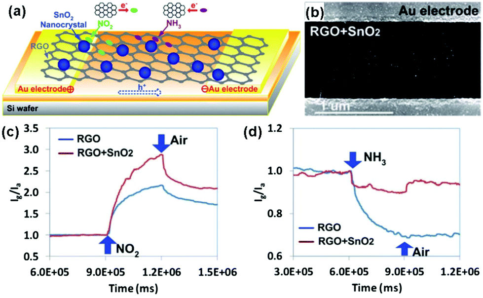 | ||
| Fig. 9 (a) Schematic of the novel gas-sensing platform using RGO nanosheets decorated with SnO2 NCs. (b) SEM image of the SnO2 NC decorated RGO bridging a pair of Au electrode fingers. Sensor responses of RGO sensors with and without SnO2 NCs toward 100 ppm NO2 (c) and 1% NH3 (d) (reproduced from ref. 112). | ||
Carbon nanotubes (CNTs), as one-dimensional structure carbon-based materials, have been reported for the detection of various gas species, including NO2, NH3, H2, organic vapor.131–135 However, the imperfect contact of CNTs with metal electrodes limited their potential application in flexible devices. Incorporating CNTs into graphene to form a hybrid composite, not only extended the application of CNTs in flexible devices, but also improved the sensing properties of graphene. For instance, Choi et al.116 developed a flexible device using CNTs/rGO hybrid films for detection of NO2 gas at room temperature. To obtain excellent contact with metal electrodes, vertically aligned CNT arrays were directly grown on rGO films by the CVD method. Significantly, the as-fabricated sensor exhibited a remarkably enhanced response compared with their counterparts based on bare graphene.
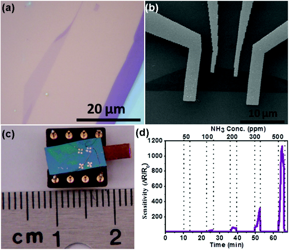
Besides, some functional polymers, including polyaniline (PANI),117–119 poly(3,4-ethylenedioxythiophene) (PEDOT),120 electrospun polymer (e.g. PVA: poly(vinyl alcohol), PEI: poly(ether imide), and PPr: polypyrene),121,122 polypyrrole (PPy),136 have been extensively studied for the chemical modification of pure graphene materials to improve their sensing performances. As a typical example, Zhang et al.118 developed a useful ammonia (NH3) gas sensor based on PANI–rGO hybrids. PANI nanoparticles were successfully anchored onto the rGO sheets by using rGO/MnO2 hybrids as both the templates and subsequent oxidants for the aniline monomer simultaneously during the process of polymerization. Fig. 10a displays an enlarged SEM image of the PANI–rGO hybrids bridging the electrode gap, and the PANI nanoparticles were distributed uniformly on the surface of rGO. Moreover, the sensor based on the PANI–rGO hybrid exhibited a much higher response toward 50 ppm NH3 than those of the pristine graphene and individual PANI nanofiber (Fig. 10b). It was revealed that the combination of rGO and PANI nanoparticles facilitated the enhancement of the sensing properties due to the synergetic behavior of the functionalities of rGO and PANI in the hybrid composites. In another example, Shi et al.122 described an ultrasensitive and selective NO2 sensor based on self-assembled graphene/electrospun polymer nanofiber (rGO/P NF) composites. These rGO/P NFs bridged the gaps of the gold digits to form conductive channels, as shown in Fig. 10c. Furthermore, this sensor exhibited high sensitivity and remarkable reversibility to NO2 gas at a concentration ranging from 150 ppb to 5 ppm at room temperature (Fig. 10d). Moreover, the LOD was experimentally measured to be as low as 150 ppb, and this value was much lower than the threshold exposure limit proposed by the American Conference of Governmental Industrial Hygienists (200 ppb).
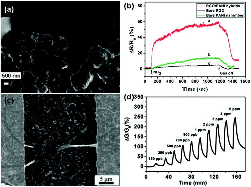 | ||
| Fig. 10 (a) An enlarged SEM image of PANI-rGO hybrid bridging electrodes. (b) The response curves of PANI-rGO hybrids, bare PANI nanofibers and bare rGO to 50 ppm NH3 at room temperature (reproduced from ref. 118). (c) SEM image of the surface of an rGO/P NF bridged interdigital electrodes. (d) Plot of response versus time for an rGO/P NF-based sensor upon exposure to NO2 with concentrations ranging from 150 ppb to 5 ppm (reproduced from ref. 122). | ||
In addition, combining ionic liquids with graphene layers is also an attractive strategy to form a highly selective gas-sensing platform. In a typical example, Ariga et al.137 prepared graphene/ionic liquid (G-IL) films by the reduction of graphene oxides in the presence of ionic liquids and subsequent layer-by-layer (LbL) assembly. The layered graphene/ionic liquid composites on quartz crystal microbalances (QCM) further demonstrated an ideal molecular discrimination for toxic aromatic hydrocarbons. This result implied the great potential of the G-IL films for practical applications in gas-sensing.
 | ||
| Fig. 11 (a) Schematic structure of both 2D and 3D devices (left), and cross-section of 3D device (right). (b) FESEM images of SU-8 pillar arrays with different heights of 40 (left) and 70 μm (right). Sensing response of rGO sensors towards (c) 5 ppm NO2 (exposure time is 15 min) and (d) 40 ppm NH3 (exposure time is 30 min) (reproduced from ref. 138). | ||
3.2 Transition metal dichalcogenide (TMD)-based gas sensors
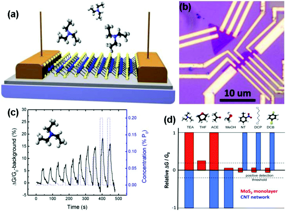 | ||
| Fig. 12 (a) MoS2 monolayer is supported on the SiO2/Si substrate and contacted with Au contact pads. Transient physisorption of molecules induces temporary conductivity changes of the sensing channel. (b) Optical image of the devices, showing the monolayer MoS2 flakes electrically contacted by multiple Au leads. (c) Device responses under a series of exposure pulses of TEA concentration increases from 0.002 to 0.2 (%P0). Inset: a model of TEA molecule. (d) Histogram of MoS2 and CNT-network sensor responses to various gases (reproduced from ref. 16). | ||
Vapour phase synthesis was considered as a promising choice to obtain high quality and large scale MoS2 films.15,18–20 As a typical example, Duesberg et al.15 developed a high-performance sensor based on MoS2 thin films prepared by sulfurization of sputtered Mo thin-films. The MoS2 thin-film sensor showed a fast response toward NH3 with experimental LOD down to 300 ppb. However, they don't immediately recover at room temperature. In another example, Zhou et al.18 performed Schottky-contacted chemical sensing using CVD-grown monolayer MoS2 synthesized with MoO3 and sulfur as starting materials. Observed from the optical microscopy (OM) image in Fig. 13a, the as-grown monolayer MoS2 on SiO2/Si substrates was a triangle-shaped material, with lateral dimensions of 5–30 μm. The MoS2 devices are also exhibited in the OM image of Fig. 13b. Furthermore, the sensing performance of the as-fabricated MoS2 FETs also demonstrated the ultrasensitive detection of NO2 down to a few ppb level and NH3 down to 1 ppm (Fig. 13c and d).
 | ||
| Fig. 13 Optical microscopy image of (a) the as-grown MoS2 monolayers on SiO2/Si substrates and (b) the MoS2 device. Real-time conductance change of MoS2 device after exposure to NO2 (c) and NH3 (d) with various concentrations. Inset in (d) is a zoom-in plot of the sensor response to low NH3 concentrations of 1, 5, and 10 ppm (reproduced from ref. 18). | ||
To achieve the highly selective and ultra-sensitive detection of volatile organic compounds (VOCs) in the lung cancer diagnosis of breath analysis, Jung et al.141 developed a tunable chemiresistor sensor by using MoS2 films and thiolated ligand (mercaptoundecanoic acid (MUA)) conjugated MoS2 films. Both films displayed high selectivity and sensitivity (down to 1 ppm) toward the representative VOC groups (ethanol, acetone, propanal, toluene, and hexane). In particular, the primitive and MUA-conjugated MoS2 sensing channels exhibited a distinctly opposite direction of sensor response toward VOCs. Therefore, it will be a promising approach to construct a versatile sensor array for application in lung cancer diagnosis, by conjugating a wide variety of thiolated ligands on the MoS2 surface. In addition, metallic nanoparticles were utilized for modifying MoS2 to improve their selectivity and sensitivity behaviors.142,143 As a typical example, Jin et al.142 described a highly sensitive H2 sensor based on the MoS2-Pd composite by a facile solvent exfoliation and drop casting method. A schematic illustration of the MoS2-Pd composite and the optical image of the sensor device are exhibited in Fig. 14a and b, respectively. In particular, upon exposure to 500–50000 ppm H2, the sensor showed a fast response and recovery time of 40 and 83 s, respectively (Fig. 14c). Furthermore, the favorable selectivity of the sensor is also demonstrated in Fig. 14d.
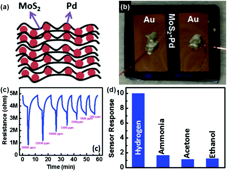 | ||
| Fig. 14 (a) Schematic illustration of the MoS2–Pd composite. (b) MoS2–Pd composite sensor device. (c) Electrical response of the MoS2–Pd composite exposed to different concentrations of H2 (500–50000 ppm) by 40 s pulses. (d) Cross-sensitivity of the MoS2–Pd composite to 50000 ppm hydrogen, 50 ppm ammonia, 50000 ppm acetone and ethanol (reproduced from ref. 142). | ||
Moreover, to avoid the unstable response of pristine MoS2 nanosheets in an air environment, Chen et al.144 developed a novel nanohybrid of the SnO2 nanocrystal-decorated crumpled MoS2 nanosheet (MoS2/SnO2). Fig. 15a illustrated schematically the preparation process of the MoS2/SnO2 nanohybrids. Furthermore, the MoS2/SnO2 sensor exhibited a reversible, reliable response and recovery characteristic toward various NO2 concentrations ranging from 0.5 ppm to 10 ppm (Fig. 15b), unlike other graphene- or carbon nanotube-based NO2 sensors that require annealing treatment, or UV illumination to facilitate recovery. The sensing response of the MoS2/SnO2 nanohybrid to various gases at a concentration of 10 ppm was also exhibited in Fig. 15c, indicating an excellent selectivity to NO2 at room temperature.
 | ||
| Fig. 15 (a) Schematic illustration of the preparation process for MoS2/SnO2 nanohybrids. Inset: photographs of the MoS2 suspension in water before and after adding SnCl4 solution. (b) Dynamic sensing response of the MoS2/SnO2 nanohybrids toward different NO2 concentrations. Inset: the enlarged sensing response curve for 0.5 ppm NO2. (c) Sensing response of the MoS2/SnO2 nanohybrid to various gases at a concentration of 10 ppm (reproduced from ref. 144). | ||
 | ||
| Fig. 16 (a) Optical image of the single-layer MoSe2. (b) SEM image of the single-layer MoSe2 sensor device supported on the SiO2/Si substrate. (c) Optical image of the as-fabricated gas sensor. (d) Sensor responses as a function of NH3 concentration (reproduced from ref. 21). | ||
For example, Li et al.22 developed a transistor based on multilayer WS2 nanoflakes using a conventional mechanical exfoliation technique. The thickness of WS2 nanoflakes is 42 nm, and the width (W) and length (L) of the sensing channel in the device is 15 μm and 20 μm, respectively (Fig. 17a and b). The charge transfer processes between adsorbed gas molecules (O2, ethanol, and NH3) and the multilayer WS2 device are schematically illustrated in Fig. 17c. When exposed to various gas atmospheres (NH3, ethanol, air, and O2), the WS2 device exhibited obviously distinct electrical and photosensitive responses (Fig. 17d). Furthermore, the gas sensitivities of the device under different conditions were also investigated in Fig. 17e. The gas sensitivity was defined as the following: S = (Igas − Ivacuum)/Ivacuum × 100%, where Igas is the current of the device in the targeted gas, and Ivacuum is the current under vacuum, VDS was fixed at 1 V. In this case, ethanol and NH3 molecules acted as electron donors to increase the electron concentration in WS2, thus leading to positive response. In particular, the device exhibited a higher sensitivity toward NH3 than that of the other gases, meaning the WS2 flakes were more sensitive to NH3 molecules. In contrast, O2 was the electron acceptor and can extract electrons from the WS2 flakes, displaying a negative response. In addition, the device exhibited higher sensitivity in O2 than that in air, due to the higher concentration of O2 acting as an electron acceptor to deplete electrons.
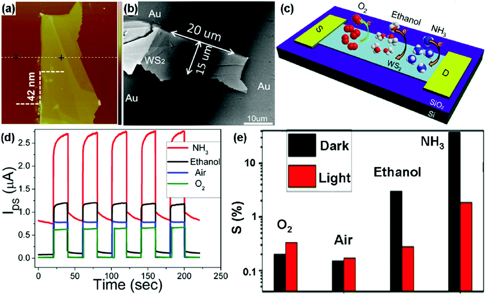 | ||
| Fig. 17 AFM (a) and SEM image (b) of the actual transistor based on multilayer WS2 nanoflakes. (c) Schematic diagram of the charge transfer process between adsorbed gas molecules and the multilayer WS2 nanoflakes transistor. (d) Time-dependent photocurrent response under various gas atmospheres. (e) The gas sensitivities (A) and current changes (B) under different conditions (reproduced from ref. 22). | ||
Very recently, Pumera et al.23 presented an impedance phase spectrum of the interdigitated gold electrode modified with chemically exfoliated 1T-WS2 for selective vapour sensing (Fig. 18a). The 1T-WS2 impedimetric device demonstrated distinct resonant frequencies with a maximum around 1 Hz in the presence of methanol vapour and around 1 kHz in the presence of water vapour (Fig. 18b). Such a well-distinguished signal allowed their selective detection even though they are present in a mixture. Moreover, the impedance device displayed highly selective detection of methanol and water vapour in the presence of excess concentrations of interference species (Fig. 18c). This selective impedimetric vapour sensing based on 1T-WS2 opens a new avenue for spectra applications in gas-sensing.
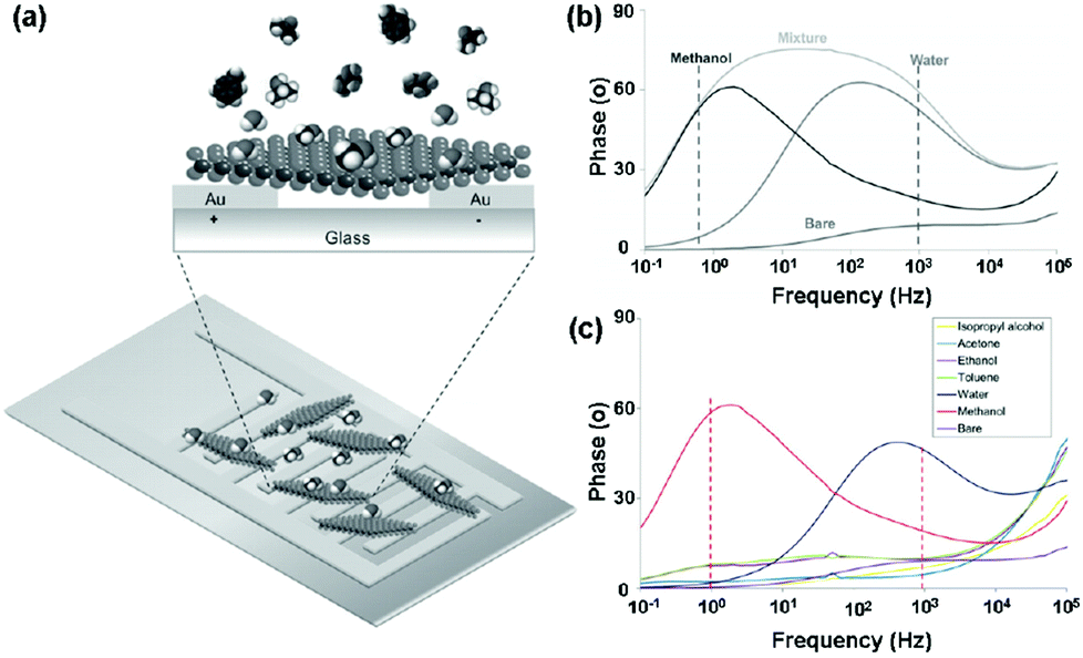 | ||
| Fig. 18 (a) Schematic representation of an interdigitated gold electrode modified with 1T-WS2 nanosheets. (b) Impedance phase spectra of 1T-WS2 device bare and toward 506 ppm methanol vapour, 26.6 g kg−1 water vapour, and in the mixture of both vapours. (c) Selectivity studies of the 1T-WS2 platform toward toluene (1394 ppm), acetone (1268 ppm), ethanol (1264 ppm), isopropyl alcohol (1259 ppm), methanol (380 ppm), and water vapour (27 g kg−1) (reproduced from ref. 23). | ||
3.3 SnS2-based gas sensors
Similar to the aspect of transition metal dichalcogenides (TMDs), tin disulfide (SnS2) exists in a layered crystal phase, which is composed of tin atoms sandwiched between two layers of hexagonally close-packed sulfur atoms.156 Compared to 2D layered MoS2, SnS2 possessed a larger electronegativity, potentially enhancing gas adsorption sites, which is demonstrated for the gas-sensing application.25,26,157 For instance, Zhang et al.25 developed a room-temperature NH3 sensor based on flower-shaped SnS2 consisting of interconnected nanosheets with thicknesses of about 40 nm prepared by a mild hydrothermal method. Fig. 19a shows a schematic diagram of a typical gas sensor. The SnS2 exhibited densely packed layers of well-edged hexagonal nanosheets with an average size of 1 μm (Fig. 19b). Upon exposure to the NH3 concentrations in the range 5 to 150 ppm, the SnS2 sensor presents a rapid response and recovery rate at room temperature (Fig. 19c), suggesting the promise of applying flower-shaped SnS2 nanostructures in the detection of NH3 molecules at room temperature. Very recently, Ou et al.26 presented a high sensitivity, excellent selective and reversible NO2 sensor based on two-dimensional (2D) SnS2 flakes at low operating temperatures. The as-obtained hexagonal 2D SnS2 flakes were prepared by a solution-based method and their lateral dimensions mainly ranged from 80 to 200 nm according to transmission electron microscopy (TEM) in Fig. 19d. Upon exposure to NO2 with concentrations ranging from 0.6 to 10 ppm, the sensor based on 2D SnS2 flakes displayed a quick response and recovery kinetics at an operating temperature of 120 °C (Fig. 19e). An excellent reversibility of the sensor is demonstrated, which has rarely been observed in other 2D material counterparts. Moreover, the 2D SnS2 flake-based sensor exhibited very strong selectivity to NO2 among other industrially meaningful concentrations of gases, including H2 (1%), CH4 (10%), CO2 (10%), and H2S (56 ppm) (Fig. 19f). The 2D SnS2-based sensor provided a feasible approach to achieve high-performance NO2 sensing for a wide range of applications in environmental monitoring, industry, and healthcare. | ||
| Fig. 19 (a) Schematic diagram of a typical gas sensor. (b) SEM image of the as-synthesized SnS2 nanoflowers. (c) Response curve on cycling between increasing concentration of NH3 gas (5–150 ppm) (reproduced from ref. 25). (d) TEM image of 2D SnS2 flakes. (e) Dynamic sensing performance of the sensor based on 2D SnS2 flakes to NO2 at concentrations ranging from 0.6 to 10 ppm under the operation temperature of 120 °C. (f) Sensor responses of 2D SnS2 flakes toward H2 (1%), CH4 (10%), CO2 (10%), H2S (56 ppm), and NO2 (10 ppm) (reproduced from ref. 26). | ||
3.4 Black phosphorus (BP)-based gas sensors
Recently, the rediscovery of black phosphorus (BP) as a new single-element 2D layered material has sparked a great deal of interest in the gas-sensing field.28–31 As a typical example, Zhou et al.29 described NO2 sensing using field-effect transistors based on multilayer BP. Fig. 20a revealed an optical image showing the multilayer BP FET used for NO2 gas detection. When exposed to NO2 gas, this BP sensor exhibited increased conductivity and excellent sensitivity for the detection of NO2 down to 5 ppb (Fig. 20b). Moreover, when this BP field-effect transistor was exposed to NO2 concentrations of 5, 10, 20, and 40 ppb, its relative conductivity change obeyed the Langmuir isotherm for molecules adsorbed on a surface (Fig. 20c). Very recently, Pumera et al.30 demonstrated a highly selective methanol sensor based on layered black phosphorus (BP) using the electrochemical impedance spectroscopy transduction method. Fig. 20d presents the device based on an interdigitated gold electrode modified with layered BP. A strong signal of the impedance phase spectra was clearly observed in the presence of methanol vapour at a resonance frequency of approximately 1 kHz. In addition, this peak enhanced with the increasing concentration of methanol vapour (Fig. 20e). The excellent selectivity of the BP sensor toward methanol was also demonstrated by recording the impedance phase at a frequency of 1 kHz after successive additions of toluene (2790 ppm), acetone (2535 ppm), chloroform (4775 ppm), dichloromethane (4262 ppm), ethanol (2519 ppm), isopropanol (2519 ppm), and water (1602 ppm) (Fig. 20f). These results implied that BP was a promising candidate for gas-sensing application. Besides, Salehi-Khojin et al.31 demonstrated an ultrasensitive and selective humidity sensor based on stacked BP flakes. The drain current of the FET-based BP sensor ranked the highest ever reported values for humidity detection with about 4 orders of magnitude as the relative humidity (RH) varied from 10% to 85%. Moreover, the BP sensor remained nearly unchanged in response after prolonged exposure (up to 3 months) to ambient conditions. | ||
| Fig. 20 (a) Optical image of the multilayer BP flake between two Ti/Au electrodes. (b) Relative conductance change (ΔG/G0) of the BP sensor toward NO2 with concentration ranging from 5 to 40 ppb. Inset: a zoomed image of exposure response to 5 ppb NO2. (c) ΔG/G0 plotted vs. NO2 concentration applied to the BP FET showing an agreement between the measured values (red squares) and the fitted Langmuir isotherm (reproduced from ref. 29). (d) Vapour sensor based on BP. (e) Impedance phase spectra of the BP device exposed to different concentrations of methanol vapour. (f) Impedance phase at 1 kHz in the presence of either methanol (1140 ppm), toluene (2790 ppm), acetone (2535 ppm), chloroform (4775 ppm), dichloromethane (4262 ppm), ethanol (2519 ppm), isopropanol (2519 ppm), or water (1602 ppm) (reproduced from ref. 30). | ||
3.5 The others
Some other layered 2D materials, such as VS2, BN, and C3N4, have been developed for gas-sensing application. Xie et al.27 presented a highly responsive humidity sensor using liquid-exfoliated VS2 nanosheets fabricated on a flexible PET substrate. Feng et al.32 reported a gas sensor based on atomic-layered BN nanosheets synthesized using the CO2-PLD technique. The as-fabricated sensor displayed a high sensitivity toward methane due to the possible reaction of CH4 molecules with B and N atoms in honeycomb-like BN nanosheets. In another example, Chen et al.33 performed a novel C-rich C3N4 for the detection of NO2 gas. The C3N4 was synthesized by a two-step thermal treatment of glucose and urea. Moreover, the C3N4 sensor possessed good sensitivity and excellent selectivity toward NO2 at room temperature, and LOD was low to 140 ppb.4. Conclusion and outlook
In this critical review, we have summarized the recent developments in the reported typical 2D layered nanomaterials for gas-sensing applications. The results demonstrate that 2D layered nanomaterials are competitive candidates for fabrication of high-performance gas sensors operated at low or room temperature due to their particular characteristics. In contrast, among these 2D layered nanomaterials, graphene has a zero band gap, and its semiconductivity fails to be modulated upon exposure to gas molecules. However, semiconductivity is an important property for a gas-sensing material, which mainly decides the potential of materials in gas sensing applications. Thus, pristine graphene materials may not be ideal for fabricating sensing devices. Fortunately, doped or modified graphene with foreign atoms and groups and functional micro/nanomaterials have been proved to be beneficial for enhancement of gas-sensing performance. Unlike graphene, metal dichalcogenides (MoS2, MoSe2, WS2, SnS2 and VS2) possess tunable band gaps dependent on their layer thickness, and their excellent semiconductivities make them attractive candidates for fabrication of gas sensors. However, up to now, there has been no reliable strategy to obtain scalable and controlled synthesis of certain layers, which hampers the development of integrated sensor research. Tables 1 and 2 summarize the important studies on gas sensors based on some typical 2D layered nanomaterials. Certainly, it is not possible for us to cover all progress in this review and there are definitely many interesting and exciting research topics waiting exploration. Some of the remaining challenges are listed as the following:(1) Improvement of response and recovery characteristics: 2D layered nanomaterial based gas sensors always exhibit extremely sluggish response and incomplete recovery to the initial state during operation at room temperature. This phenomenon is attributed to their charge transfer sensing mechanism. To improve these issues, the following strategies are worthy of attention: developing novel gas-sensing nanomaterials, surface functionalization and doping, accurate fabrication techniques, unique measurement techniques, and optimizing device geometry.
(2) Fabrication of gas sensors: most of the gas sensors are fabricated by a drop casting or microfabrication process. However, these processes not only are complicated and time-consuming, but also fail to display the intrinsic properties of the channel materials. Thus, it still remains a huge challenge to develop a facile, effective and reliable strategy to fabricate gas sensors.
(3) Practical application of gas sensors: after development for several decades, sensitivity, has shown great improvement, and is no longer the main concern of a gas sensor, while the selectivity and stability are still great challenges in practical applications. For gas sensors based on 2D layered nanomaterials, they always exhibit a cross-response to several kinds of reactive gases, leading to poor selectivity. Furthermore, most of them possess unstable response signals while being operated at low or room temperature. To address these issues, several strategies may be adopted, including surface modification, functional doping, and optimizing test conditions.
| No. | Graphene materials | Sensor type | Detected gas | Sensitivity | LOD | Ref. |
|---|---|---|---|---|---|---|
| 1 | Mechanically exfoliated G | Hall geometry | NO2 | ΔR = 2.5 Ω (1 electron) | 1 molecule | 64 |
| 2 | CVD-grown G | FET | NO2 | ΔR/R = 12.49% (5 ppm) | 6.87 ppb | 68 |
| 3 | CVD-grown G | FET | NO2 | ΔI/I0 = 1.67 ppm−1 | 300 ppt | 76 |
| 4 | Epitaxially grown G | Chemiresistor | NO2 | ΔG/G = −9% (18 ppm, Si-face) | 81 | |
| ΔG/G = 4% (18 ppm, C-face) | ||||||
| 5 | Hydrazine-reduced GO | Chemiresistor | DNT | ΔR/R = −0.028% (52 ppb) | 98 | |
| 6 | Vc-reduced GO | Chemiresistor | NO2 | ΔR/R = 6% (10 ppm) | 400 ppt | 100 |
| 7 | PPD-reduced GO | Chemiresistor | DMMP | ΔR/R = 8% (20 ppm) | 101 | |
| 8 | NaBH4-reduced GO | Chemiresistor | NH3 | ΔR/R = 5.5% (200 ppm) | 102 | |
| 9 | Sulfonated rGO | Chemiresistor | NO2 | ΔG/G = 0.443 ppm−1 | 3.6 ppm | 48 |
| 10 | Ag-S-RGO | Chemiresistor | NO2 | ΔR/R = −45% (50 ppm) | 103 | |
| 11 | Pt–G | Chemiresistor | H2 | ΔR/R = 16% (4%) | 105 | |
| 12 | Pd-RGO | Chemiresistor | NO | ΔG/G = 4% (2 ppb) | 106 | |
| 13 | AgNW coated rGO | Chemiresistor | NH3 | ΔR/R = 3% (15 ppm) | 107 | |
| 14 | SnO2-RGO | FET | NO2 | I g/Ia = 1.11 (1 ppm) | 112 | |
| 15 | Cu2O-rGO | Chemiresistor | NO2 | ΔI/I0 = 67.8% (2 ppm) | 64 ppb | 114 |
| 16 | CuO–ZnO/G | Chemiresistor | Acetone | R a/Rg = 9.4 (10 ppm) | 115 | |
| 17 | ZnO QDs/G | Chemiresistor | Formaldehyde | ΔG/G = 1.1 (100 ppm) | 129 | |
| 18 | Pt–SnO2/G | Chemiresistor | H2 | ΔR/R = 2 (1%) | 43 | |
| 19 | CNT/rGO | FET | NO2 | ΔR/R = 20% (20 ppm) | 116 | |
| 20 | PANI/G | Chemiresistor | NH3 | ΔR/R = 32.5% (10 ppm) | 118 | |
| 21 | PSS-PANI/G | Chemiresistor | H2S | ΔR/R = 60% (20 ppm) | 1 ppm | 119 |
| 22 | PEDOT/G | FET | NO2 | ΔR/R = 20% (2 ppm) | 500 ppb | 120 |
| 23 | P NFs/G | Chemiresistor | NO2 | ΔR/R = 1.03 ppm−1 | 150 ppb | 122 |
| No. | Materials | Sensor type | Detected gas | LOD | Ref. |
|---|---|---|---|---|---|
| 1 | 2 layer MoS2 | FET | NO | 0.3 ppm | 14 |
| 2 | MoS2 thin film | FET | NH3 | 300 ppb | 15 |
| 3 | MoS2 monolayer | Chemiresistor | Triethylamine | 10 ppb | 16 |
| 4 | 2, 5 layered MoS2 | FET | NH3, NO2 | 17 | |
| 5 | MoS2 monolayer | FET | NH3, NO2 | 1 ppm, 10 ppb | 18 |
| 6 | Thiolated ligand MoS2 | Chemiresistor | VOCs | <1 ppm | 141 |
| 7 | Pd–MoS2 | Chemiresistor | H2 | 500 ppm | 142 |
| 8 | Pt–MoS2 | FET | NO2 | 0.5 ppm | 143 |
| 9 | SnO2–MoS2 | FET | NO2 | 0.5 ppm | 144 |
| 10 | Atomic layered MoS2 | FET | NH3, NO2 | 1 ppm, 1 ppm | 20 |
| 11 | Monolayer MoSe2 | FET | NH3 | 50 ppm | 21 |
| 12 | Multilayer WS2 | FET | NH3, ethanol | 22 | |
| 13 | Metallic 1T-WS2 | Impedance | Methanol | 5.6 ppm | 23 |
| 14 | Flower-shaped SnS2 | Chemiresistor | NH3 | 5 ppm | 25 |
| 15 | 2D SnS2 flakes | Chemiresistor | NO2 | 20–30 ppb | 26 |
| 16 | SnS2–SnO2 nanohybrids | Chemiresistor | NH3 | 10 ppm | 157 |
| 17 | Black phosphorus | FET | NO2 | 5 ppb | 29 |
| 18 | Black phosphorus | Impedance | Methanol | 28 ppm | 30 |
| 19 | BN nanosheets | Chemiresistor | CH4 | 32 | |
| 20 | C-rich C3N4 | Chemiresistor | NO2 | 140 ppb | 33 |
Acknowledgements
This work was supported by the National Nature Science Foundation of China (21322106, 21501060 and 51472097), the National Basic Research Program of China (973 program, 2015CB932600), the Program for New Century Excellent Talents in University (NCET-13-0227), the Program for HUST Interdisciplinary Innovation Team and the Fundamental Research Funds for the Central University. The authors are indebted for the kind permission from the corresponding publishers/authors to reproduce their materials, especially figures, used in this article.References
- X. Zhou, S. Lee, Z. C. Xu and J. Yoon, Chem. Rev., 2015, 115, 7944–8000 CrossRef CAS PubMed.
- A. Tricoli, M. Righettoni and A. Teleki, Angew. Chem., Int. Ed., 2010, 49, 7632–7659 CrossRef CAS PubMed.
- S. Su, W. H. Wu, J. M. Gao, J. X. Lu and C. H. Fan, J. Mater. Chem., 2012, 22, 18101–18110 RSC.
- Y. F. Sun, S. B. Liu, F. L. Meng, J. Y. Liu, Z. Jin, L. T. Kong and J. H. Liu, Sensors, 2012, 12, 2610–2631 CrossRef CAS PubMed.
- G. F. Fine, L. M. Cavanagh, A. Afonja and R. Binions, Sensors, 2010, 10, 5469–5502 CrossRef CAS PubMed.
- H. Wang, K. Kalantar-Zadeh, A. Kis, J. N. Coleman and M. S. Strano, Nat. Nanotechnol., 2012, 7, 699–712 CrossRef PubMed.
- G. Fiori, F. Bonaccorso, G. Iannaccone, T. Palacios, D. Neumaier, A. Seabaugh, S. K. Banerjee and L. Colombo, Nat. Nanotechnol., 2014, 9, 768–779 CrossRef CAS PubMed.
- C. N. R. Rao, H. S. S. Ramakrishna Matte and U. Maitra, Angew. Chem., Int. Ed., 2013, 52, 13162–13185 CrossRef CAS PubMed.
- X. Zhou, L. Gan, W. M. Tian, Q. Zhang, S. Y. Jin, H. Q. Li, Y. Bando, D. Golberg and T. Y. Zhai, Adv. Mater., 2015, 27, 8035–8041 CrossRef CAS PubMed.
- F. Schwierz, J. Pezoldt and R. Granzner, Nanoscale, 2015, 7, 8261–8283 RSC.
- Y. X. Liu, X. C. Dong and P. Chen, Chem. Soc. Rev., 2012, 41, 2283–2307 RSC.
- Q. Y. He, S. X. Wu, Z. Y. Yin and H. Zhang, Chem. Sci., 2012, 3, 1764–1772 RSC.
- W. J. Yuan and G. Q. Shi, J. Mater. Chem. A, 2013, 1, 10078–10091 CAS.
- H. Li, Z. Y. Yin, Q. Y. He, X. Huang, G. Lu, D. W. H. Fam, A. I. Y. Tok, Q. Zhang and H. Zhang, Small, 2012, 8, 63–67 CrossRef CAS PubMed.
- K. Lee, R. Gatensby, N. McEvoy, T. Hallam and G. S. Duesberg, Adv. Mater., 2013, 25, 6699–6702 CrossRef CAS PubMed.
- F. K. Perkins, A. L. Friedman, E. Cobas, P. M. Campbell, G. G. Jernigan and B. T. Jonker, Nano Lett., 2013, 13, 668–673 CrossRef CAS PubMed.
- D. J. Late, Y. K. Huang, B. Liu, J. Acharya, S. N. Shirodkar, J. J. Luo, A. M. Yan, D. Charles, U. V. Waghmare, V. P. Dravid and C. N. R. Rao, ACS Nano, 2013, 7, 4879–4891 CrossRef CAS PubMed.
- B. L. Liu, L. Chen, G. Liu, A. N. Abbas, M. Fathi and C. W. Zhou, ACS Nano, 2014, 8, 5304–5314 CrossRef CAS PubMed.
- B. Cho, M. G. Hahm, M. Choi, J. Yoon, A. R. Kim, Y. J. Lee, S. G. Park, J. D. Kwon, C. S. Kim, M. Song, Y. Jeong, K. S. Nam, S. Lee, T. J. Yoo, C. G. Kang, B. H. Lee, H. C. Ko, P. M. Ajayan and D. H. Kim, Sci. Rep., 2015, 5, 8052 CrossRef CAS PubMed.
- B. Cho, A. R. Kim, Y. Park, J. Yoon, Y. J. Lee, S. Lee, T. J. Yoo, C. G. Kang, B. H. Lee, H. C. Ko, D. H. Kim and M. G. Hahm, ACS Appl. Mater. Interfaces, 2015, 7, 2952–2959 CAS.
- D. J. Late, T. Doneux and M. Bougouma, Appl. Phys. Lett., 2014, 105, 233103 CrossRef.
- N. J. Huo, S. X. Yang, Z. M. Wei, S. S. Li, J. B. Xia and J. B. Li, Sci. Rep., 2014, 4, 5209 CAS.
- C. C. Mayorga-Martinez, A. Ambrosi, A. Y. S. Eng, Z. Sofer and M. Pumera, Adv. Funct. Mater., 2015, 25, 5611–5616 CrossRef CAS.
- M. O'Brien, K. Lee, R. Morrish, N. C. Berner, N. McEvoy, C. A. Wolden and G. S. Duesberg, Chem. Phys. Lett., 2014, 615, 6–10 CrossRef.
- W. D. Shi, L. H. Huo, H. S. Wang, H. J. Zhang, J. H. Yang and P. H. Wei, Nanotechnology, 2006, 17, 2918–2924 CrossRef CAS.
- J. Z. Ou, W. Y. Ge, B. Carey, T. Daeneke, A. Rotbart, W. Shan, Y. C. Wang, Z. Q. Fu, A. F. Chrimes, W. Wlodarski, S. P. Russo, Y. X. Li and K. Kalantar-zadeh, ACS Nano, 2015, 9, 10313–10323 CrossRef CAS PubMed.
- J. Feng, L. L. Peng, C. Z. Wu, X. Sun, S. L. Hu, C. W. Lin, J. Dai, J. L. Yang and Y. Xie, Adv. Mater., 2012, 24, 1969–1974 CrossRef CAS PubMed.
- L. Z. Kou, T. Frauenheim and C. F. Chen, J. Phys. Chem. Lett., 2014, 5, 2675–2681 CrossRef CAS PubMed.
- A. N. Abbas, B. L. Liu, L. Chen, Y. Q. Ma, S. Cong, N. Aroonyadet, M. Kopf, T. Nilges and C. W. Zhou, ACS Nano, 2015, 9, 5618–5624 CrossRef CAS PubMed.
- C. C. Mayorga-Martinez, Z. Sofer and M. Pumera, Angew. Chem., Int. Ed., 2015, 54, 14317–14320 CrossRef CAS.
- P. Yasaei, A. Behranginia, T. Foroozan, M. Asadi, K. Kim, F. Khalili-Araghi and A. Salehi-Khojin, ACS Nano, 2015, 9, 9898–9905 CrossRef CAS PubMed.
- M. Sajjad and P. Feng, Mater. Res. Bull., 2014, 49, 35–38 CrossRef CAS.
- D. H. Wang, W. Gu, Y. W. Zhang, Y. Hu, T. Zhang, X. M. Tao and W. Chen, RSC Adv., 2014, 4, 18003–18006 RSC.
- Q. M. Ji, S. B. Yoon, J. P. Hill, A. Vinu, J. S. Yu and K. Ariga, J. Am. Chem. Soc., 2009, 131, 4220–4221 CrossRef CAS PubMed.
- K. Ariga, A. Vinu, Q. M. Ji, O. Ohmori, J. P. Hill, S. Acharya, J. Koike and S. Shiratori, Angew. Chem., Int. Ed., 2008, 47, 7254–7257 CrossRef CAS PubMed.
- Z. Li, J. Lu, S. D. Li, S. H. Qin and Y. M. Qin, Adv. Mater., 2012, 24, 6053–6057 CrossRef CAS PubMed.
- B. R. Takulapalli, G. M. Laws, P. A. Liddell, J. Andreasson, Z. Erno, D. Gust and T. J. Thornton, J. Am. Chem. Soc., 2008, 130, 2226–2233 CrossRef CAS PubMed.
- F. Naso, F. Babudri, D. Colangiuli, G. M. Farinola, F. Quaranta, R. Rella, R. Tafuro and L. Valli, J. Am. Chem. Soc., 2003, 125, 9055–9061 CrossRef CAS PubMed.
- M. C. Tanese, G. M. Farinola, B. Pignataro, L. Valli, L. Giotta, S. Conoci, P. Lang, D. Colangiuli, F. Babudri, F. Naso, L. Sabbatini, P. G. Zambonin and L. Torsi, Chem. Mater., 2006, 18, 778–784 CrossRef CAS.
- K. Ariga, Y. Yamauchi, G. Rydzek, Q. M. Ji, Y. Yonamine, K. C. W. Wu and J. P. Hill, Chem. Lett., 2014, 43, 36–68 CrossRef CAS.
- K. Ariga, Y. Yamauchi, T. Mori and J. P. Hill, Adv. Mater., 2013, 25, 6477–6512 CrossRef CAS PubMed.
- X. Huang, X. Y. Qi, F. Boey and H. Zhang, Chem. Soc. Rev., 2012, 41, 666–686 RSC.
- Y. W. Zhu, S. Murali, W. W. Cai, X. S. Li, J. W. Suk, J. R. Potts and R. S. Ruoff, Adv. Mater., 2010, 22, 3906–3924 CrossRef CAS.
- X. Huang, Z. Y. Zeng and H. Zhang, Chem. Soc. Rev., 2013, 42, 1934–1946 RSC.
- Y. F. Sun, S. Gao, F. C. Lei and Y. Xie, Chem. Soc. Rev., 2015, 44, 623–636 RSC.
- P. K. Kannan, D. J. Late, H. Morgan and C. S. Rout, Nanoscale, 2015, 7, 13293–13312 RSC.
- G. H. Yang, C. Z. Zhu, D. Du, J. J. Zhu and Y. H. Lin, Nanoscale, 2015, 7, 14217–14231 RSC.
- W. J. Yuan, A. R. Liu, L. Huang, C. Li and G. Q. Shi, Adv. Mater., 2013, 25, 766–771 CrossRef CAS PubMed.
- P. A. Russo, N. Donato, S. G. Leonardi, S. Baek, D. E. Conte, G. Neri and N. Pinna, Angew. Chem., Int. Ed., 2012, 51, 11053–11057 CrossRef CAS PubMed.
- W. Yang, P. Wan, X. D. Zhou, J. M. Hu, Y. F. Guan and L. Feng, ACS Appl. Mater. Interfaces, 2014, 6, 21093–23100 CAS.
- L. Li, S. J. He, M. M. Liu, C. M. Zhang and W. Chen, Anal. Chem., 2015, 87, 1638–1645 CrossRef CAS PubMed.
- H. Zhang, J. C. Feng, T. Fei, S. Liu and T. Zhang, Sens. Actuators, B, 2014, 190, 472–478 CrossRef CAS.
- H. Meng, W. Yang, K. Ding, L. Feng and Y. F. Guan, J. Mater. Chem. A, 2015, 3, 1174–1181 CAS.
- K. Anand, O. Singh, M. P. Singh, J. Kaur and R. C. Singh, Sens. Actuators, B, 2014, 195, 409–415 CrossRef CAS.
- D. Jariwala, V. K. Sangwan, L. J. Lauhon, T. J. Marks and M. C. Hersam, ACS Nano, 2014, 8, 1102–1120 CrossRef CAS PubMed.
- Z. Y. Zhang, X. M. Zou, L. Xu, L. Liao, W. Liu, J. Ho, X. H. Xiao, C. Z. Jiang and J. C. Li, Nanoscale, 2015, 7, 10078–10084 RSC.
- Y. P. Dan, Y. Lu, N. J. Kybert, Z. T. Luo and A. T. Johnson, Nano Lett., 2009, 9, 1472–1475 CrossRef CAS PubMed.
- B. Kumar, K. Min, M. Bashirzadeh, A. B. Farimani, M. H. Bae, D. Estrada, Y. D. Kim, P. Yasaei, Y. D. Park, E. Pop, N. R. Aluru and A. Salehi-Khojin, Nano Lett., 2013, 13, 1962–1968 CrossRef CAS PubMed.
- R. Arsat, M. Breedon, M. Shafiei, P. G. Spizziri, S. Gilje, R. B. Kaner, K. Kalantar-zadeh and W. Wlodarski, Chem. Phys. Lett., 2009, 467, 344–347 CrossRef CAS.
- S. Rumyantsev, G. X. Liu, M. S. Shur, R. A. Potyrailo and A. A. Balandin, Nano Lett., 2012, 12, 2294–2298 CrossRef CAS PubMed.
- X. Huang, Z. Y. Yin, S. X. Wu, X. Y. Qi, Q. Y. He, Q. C. Zhang, Q. Y. Yan, F. Boey and H. Zhang, Small, 2011, 7, 1876–1902 CrossRef CAS PubMed.
- Y. M. Lin and P. Avouris, Nano Lett., 2008, 8, 2119–2125 CrossRef CAS PubMed.
- Z. G. Cheng, Q. Li, Z. J. Li, Q. Y. Zhou and Y. Fang, Nano Lett., 2010, 10, 1864–1868 CrossRef CAS PubMed.
- F. Schedin, A. K. Geim, S. V. Morozov, E. W. Hill, P. Blake, M. I. Katsnelson and K. S. Novoselov, Nat. Mater., 2007, 6, 652–655 CrossRef CAS PubMed.
- K. S. Novoselov, A. K. Geim, S. V. Morozov, D. Jiang, M. I. Katsnelson, I. V. Grigorieva, S. V. Dubonos and A. A. Firsov, Nature, 2005, 438, 197–200 CrossRef CAS PubMed.
- Y. B. Zhang, Y. W. Tan, H. L. Stormer and P. Kim, Nature, 2005, 438, 201–204 CrossRef CAS PubMed.
- X. S. Li, W. W. Cai, J. An, S. Kim, J. Nah, D. X. Yang, R. Piner, A. Velamakanni, I. Jung, E. Tutuc, S. K. Banerjee, L. Colombo and R. S. Ruoff, Science, 2009, 324, 1312–1314 CrossRef CAS PubMed.
- Y. H. Kim, S. J. Kim, Y. J. Kim, Y. S. Shim, S. Y. Kim, B. H. Hong and H. W. Jang, ACS Nano, 2015, 9, 10453–10460 CrossRef CAS PubMed.
- Y. J. Ren, C. F. Zhu, W. W. Cai, H. F. Li, H. X. Ji, I. Kholmanov, Y. P. Wu, R. D. Piner and R. S. Ruoff, Appl. Phys. Lett., 2012, 100, 163114 CrossRef.
- F. Yavari, E. Castillo, H. Gullapalli, P. M. Ajayan and N. Koratkar, Appl. Phys. Lett., 2012, 100, 203120 CrossRef.
- R. K. Paul, S. Badhulika, N. M. Saucedo and A. Mulchandani, Anal. Chem., 2012, 84, 8171–8178 CrossRef CAS PubMed.
- Y. W. Yu, L. Gan, X. F. Wan and T. Y. Zhai, RSC Adv., 2015, 5, 56293–56298 RSC.
- F. Yavari, Z. Chen, A. V. Thomas, W. Ren, H. M. Cheng and N. Koratkar, Sci. Rep., 2011, 1, 166 CrossRef PubMed.
- J. W. Suk, A. Kitt, C. W. Magnuson, Y. F. Hao, S. Ahmed, J. An, A. K. Swan, B. B. Goldberg and R. S. Ruoff, ACS Nano, 2011, 5, 6916–6924 CrossRef CAS PubMed.
- L. G. P. Martins, Y. Song, T. Y. Zeng, M. S. Dresselhaus, J. Kong and P. T. Araujo, Proc. Natl. Acad. Sci. U. S. A., 2013, 110, 17762–17767 CrossRef CAS PubMed.
- S. Kumar, S. Kaushik, R. Pratap and S. Raghavan, ACS Appl. Mater. Interfaces, 2015, 7, 2189–2194 CAS.
- C. Berger, Z. M. Song, X. B. Li, X. S. Wu, N. Brown, C. Naud, D. Mayou, T. B. Li, J. Hass, A. N. Marchenkov, E. H. Conrad, P. N. First and W. A. d. Heer, Science, 2006, 312, 1191–1196 CrossRef CAS PubMed.
- M. Qazi, M. W. K. Nomani, M. V. S. Chandrashekhar, V. B. Shields, M. G. Spencer and G. Koley, Appl. Phys. Express, 2010, 3, 075101–075103 CrossRef.
- S. Y. Zhou, G.-H. Gweon, A. V. Fedorov, P. N. First, W. A. d. Heer, D.-H. Lee, F. Guinea, A. H. C. Neto and A. Lanzara, Nat. Mater., 2007, 6, 770–775 CrossRef CAS PubMed.
- J. Y. Dai and J. M. Yuan, Chem. Phys., 2012, 405, 161–166 CrossRef CAS.
- M. W. K. Nomani, R. Shishir, M. Qazi, D. Diwan, V. B. Shields, M. G. Spencer, G. S. Tompa, N. M. Sbrockey and G. Koley, Sens. Actuators, B, 2010, 150, 301–307 CrossRef CAS.
- R. Pearce, T. Iakimov, M. Andersson, L. Hultman, A. L. Spetz and R. Yakimova, Sens. Actuators, B, 2011, 155, 451–455 CrossRef CAS.
- S. Park and R. S. Ruoff, Nat. Nanotechnol., 2009, 4, 217–224 CrossRef CAS PubMed.
- D. R. Dreyer, S. Park, C. W. Bielawski and R. S. Ruoff, Chem. Soc. Rev., 2010, 39, 228–240 RSC.
- C. K. Chua and M. Pumera, Chem. Soc. Rev., 2014, 43, 291–312 RSC.
- D. A. Dikin, S. Stankovich, E. J. Zimney, R. D. Piner, G. H. B. Dommett, G. Evmenenko, S. T. Nguyen and R. S. Ruoff, Nature, 2007, 448, 457–460 CrossRef CAS PubMed.
- D. C. Marcano, D. V. Kosynkin, J. M. Berlin, A. Sinitskii, Z. Z. Sun, A. Slesarev, L. B. Alemany, W. Lu and J. M. Tour, ACS Nano, 2010, 4, 4806–4814 CrossRef CAS PubMed.
- J. Kim, L. J. Cote and J. X. Huang, Acc. Chem. Res., 2012, 45, 1356–1364 CrossRef CAS.
- J. Kim, L. J. Cote, F. Kim, W. Yuan, K. R. Shull and J. X. Huang, J. Am. Chem. Soc., 2010, 132, 8180–8186 CrossRef CAS PubMed.
- Q. Xu, H. Xu, J. R. Chen, Y. Z. Lv, C. B. Dong and T. S. Sreeprasad, Inorg. Chem. Front., 2015, 2, 417–424 RSC.
- A. Bagri, C. Mattevi, M. Acik, Y. J. Chabal, M. Chhowalla and V. B. Shenoy, Nat. Chem., 2010, 2, 581–587 CrossRef CAS PubMed.
- L. Liao, H. L. Peng and Z. F. Liu, J. Am. Chem. Soc., 2014, 136, 12194–12200 CrossRef CAS PubMed.
- Y. R. Choi, Y.-G. Yoon, K. S. Choi, J. H. Kang, Y.-S. Shim, Y. H. Kim, H. J. Chang, J.-H. Lee, C. R. Park, S. Y. Kim and H. W. Jang, Carbon, 2015, 91, 178–187 CrossRef CAS.
- S. F. Pei and H. M. Cheng, Carbon, 2012, 50, 3210–3228 CrossRef CAS.
- R. L. D. Whitby, ACS Nano, 2014, 8, 9733–9754 CrossRef CAS PubMed.
- T. Kuila, A. K. Mishra, P. Khanra, N. H. Kim and J. H. Lee, Nanoscale, 2013, 5, 52–71 RSC.
- J. T. Robinson, F. K. Perkins, E. S. Snow, Z. Q. Wei and P. E. Sheehan, Nano Lett., 2008, 8, 3137–3140 CrossRef CAS PubMed.
- J. D. Fowler, M. J. Allen, V. C. Tung, Y. Yang, R. B. Kaner and B. H. Weiller, ACS Nano, 2009, 3, 301–306 CrossRef CAS PubMed.
- G. H. Lu, S. Park, K. H. Yu, R. S. Ruoff, L. E. Ocola, D. Rosenmann and J. H. Chen, ACS Nano, 2011, 5, 1154–1164 CrossRef CAS PubMed.
- V. Dua, S. P. Surwade, S. Ammu, S. R. Agnihotra, S. Jain, K. E. Roberts, S. Park, R. S. Ruoff and S. K. Manohar, Angew. Chem., Int. Ed., 2010, 49, 2154–2157 CrossRef CAS PubMed.
- N. T. Hu, Y. Y. Wang, J. Chai, R. G. Gao, Z. Yang, E. S. Kong and Y. F. Zhang, Sens. Actuators, B, 2012, 163, 107–114 CrossRef CAS.
- R. Ghosh, A. Midya, S. Santra, S. K. Ray and P. K. Guha, ACS Appl. Mater. Interfaces, 2013, 5, 7599–7603 CAS.
- L. Huang, Z. P. Wang, J. K. Zhang, J. L. Pu, Y. J. Lin, S. H. Xu, L. Shen, Q. Chen and W. Z. Shi, ACS Appl. Mater. Interfaces, 2014, 6, 7426–7433 CAS.
- F. Niu, J. M. Liu, L. M. Tao, W. Wang and W. G. Song, J. Mater. Chem. A, 2013, 1, 6130–6133 CAS.
- A. Kaniyoor, R. I. Jafri, T. Arockiadoss and S. Ramaprabhu, Nanoscale, 2009, 1, 382–386 RSC.
- W. W. Li, X. M. Geng, Y. F. Guo, J. Z. Rong, Y. P. Gong, L. Q. Wu, X. M. Zhang, P. Li, J. B. Xu, G. S. Cheng, M. T. Sun and L. W. Liu, ACS Nano, 2011, 5, 6955–6961 CrossRef CAS PubMed.
- Y. Pak, S. M. Kim, H. Jeong, C. G. Kang, J. S. Park, H. Song, R. Lee, N. Myoung, B. H. Lee, S. Seo, J. T. Kim and G. Y. Jung, ACS Appl. Mater. Interfaces, 2014, 6, 13293–13298 CAS.
- D. H. Shin, J. S. Lee, J. Jun, J. H. An, S. G. Kim, K. H. Cho and J. Jang, Sci. Rep., 2015, 5, 12294 CrossRef PubMed.
- Q. T. Tran, H. T. M. Hoa, D.-H. Yoo, T. V. Cuong, S. H. Hur, J. S. Chung, E. J. Kim and P. A. Kohl, Sens. Actuators, B, 2014, 194, 45–50 CrossRef CAS.
- V. Tjoa, W. Jun, V. Dravid, S. Mhaisalkar and N. Mathews, J. Mater. Chem., 2011, 21, 15593–15599 RSC.
- B. Cho, J. Yoon, M. G. Hahm, D. H. Kim, A. R. Kim, Y. H. Kahng, S. W. Park, Y. J. Lee, S. G. Park, J. D. Kwon, C. S. Kim, M. Song, Y. Jeong, K. S. Nam and H. C. Ko, J. Mater. Chem. C, 2014, 2, 5280–5285 RSC.
- S. Mao, S. M. Cui, G. H. Lu, K. H. Yu, Z. H. Wen and J. H. Chen, J. Mater. Chem., 2012, 22, 11009–11013 RSC.
- X. Q. An, J. C. Yu, Y. Wang, Y. M. Hu, X. L. Yu and G. J. Zhang, J. Mater. Chem., 2012, 22, 8525–8531 RSC.
- S. Deng, V. Tjoa, H. M. Fan, H. R. Tan, D. C. Sayle, M. Olivo, S. Mhaisalkar, J. Wei and C. H. Sow, J. Am. Chem. Soc., 2012, 134, 4905–4917 CrossRef CAS PubMed.
- C. Wang, J. W. Zhu, S. M. Liang, H. P. Bi, Q. F. Han, X. H. Liu and X. Wang, J. Mater. Chem. A, 2014, 2, 18635–18643 CAS.
- H. Y. Jeong, D. S. Lee, H. K. Choi, D. H. Lee, J. E. Kim, J. Y. Lee, W. J. Lee, S. O. Kim and S. Y. Choi, Appl. Phys. Lett., 2010, 96, 213105 CrossRef.
- L. Al-Mashat, K. Shin, K. Kalantar-zadeh, J. D. Plessis, S. H. Han, R. W. Kojima, R. B. Kaner, D. Li, X. L. Gou, S. J. Ippolito and W. Wlodarski, J. Phys. Chem. C, 2010, 114, 16168–16173 CAS.
- X. L. Huang, N. T. Hu, R. G. Gao, Y. Yu, Y. Y. Wang, Z. Yang, E. Siu-Wai Kong, H. Wei and Y. F. Zhang, J. Mater. Chem., 2012, 22, 22488–22495 RSC.
- S. Cho, J. S. Lee, J. Jun, S. G. Kim and J. Jang, Nanoscale, 2014, 6, 15181–15195 RSC.
- Y. J. Yang, S. B. Li, W. Y. Yang, W. T. Yuan, J. H. Xu and Y. D. Jiang, ACS Appl. Mater. Interfaces, 2014, 6, 13807–13814 CAS.
- L. Zhang, C. Li, A. R. Liu and G. Q. Shi, J. Mater. Chem., 2012, 22, 8438–8443 RSC.
- W. J. Yuan, L. Huang, Q. H. Zhou and G. Q. Shi, ACS Appl. Mater. Interfaces, 2014, 6, 17003–17008 CAS.
- M. M. Arafat, B. Dinan, S. A. Akbar and A. S. M. A. Haseeb, Sensors, 2012, 12, 7207–7258 CrossRef CAS PubMed.
- K. J. Choi and H. W. Jang, Sensors, 2010, 10, 4083–4099 CrossRef CAS PubMed.
- E. Comini, C. Baratto, I. Concina, G. Faglia, M. Falasconi, M. Ferroni, V. Galstyan, E. Gobbi, A. Ponzoni, A. Vomiero, D. Zappa, V. Sberveglieri and G. Sberveglieri, Sens. Actuators, B, 2013, 179, 3–20 CrossRef CAS.
- Y. B. Hahn, R. Ahmad and N. Tripathy, Chem. Commun., 2012, 48, 10369–10385 RSC.
- Y. Yang, C. G. Tian, L. Sun, R. J. Lü, W. Zhou, K. Y. Shi, K. Kan, J. C. Wang and H. G. Fu, J. Mater. Chem. A, 2013, 1, 12742–12749 CAS.
- L. S. Zhou, F. P. Shen, X. K. Tian, D. H. Wang, T. Zhang and W. Chen, Nanoscale, 2013, 5, 1564–1569 RSC.
- Q. W. Huang, D. W. Zeng, H. Y. Li and C. S. Xie, Nanoscale, 2012, 4, 5651–5658 RSC.
- R. K. Mishra, S. B. Upadhyay, A. Kushwaha, T. H. Kim, G. Murali, R. Verma, M. Srivastava, J. Singh, P. P. Sahay and S. H. Lee, Nanoscale, 2015, 7, 11971–11979 RSC.
- S. Chopra, K. McGuire, N. Gothard, A. M. Rao and A. Pham, Appl. Phys. Lett., 2003, 83, 2280 CrossRef CAS.
- J. Li, Y. J. Lu, Q. Ye, M. Cinke, J. Han and M. Meyyappan, Nano Lett., 2003, 3, 929–933 CrossRef CAS.
- S. Hanna Varghese, R. Nair, B. G. Nair, T. Hanajiri, T. Maekawa, Y. Yoshida and D. Sakthi Kumar, Curr. Nanosci., 2010, 6, 331–346 CrossRef.
- Y. Battie, O. Ducloux, P. Thobois, N. Dorval, J. S. Lauret, B. Attal-Trétout and A. Loiseau, Carbon, 2011, 49, 3544–3552 CrossRef CAS.
- S. Dhall, N. Jaggi and R. Nathawat, Sens. Actuators, A, 2013, 201, 321–327 CrossRef CAS.
- H. Bai, K. X. Sheng, P. F. Zhang, C. Li and G. Q. Shi, J. Mater. Chem., 2011, 21, 18653–18658 RSC.
- Q. M. Ji, I. Honma, S. M. Paek, M. Akada, J. P. Hill, A. Vinu and K. Ariga, Angew. Chem., Int. Ed., 2010, 49, 9737–9739 CrossRef CAS PubMed.
- L. T. Duy, D. J. Kim, T. Q. Trung, V. Q. Dang, B. Y. Kim, H. K. Moon and N. E. Lee, Adv. Funct. Mater., 2015, 25, 883–890 CrossRef CAS.
- R. Ganatra and Q. Zhang, ACS Nano, 2014, 8, 4074–4099 CrossRef CAS.
- Q. Y. He, Z. Y. Zeng, Z. Y. Yin, H. Li, S. X. Wu, X. Huang and H. Zhang, Small, 2012, 8, 2994–2999 CrossRef CAS PubMed.
- J. S. Kim, H. W. Yoo, H. O. Choi and H. T. Jung, Nano Lett., 2014, 14, 5941–5947 CrossRef CAS PubMed.
- C. Kuru, C. Choi, A. Kargar, D. Choi, Y. J. Kim, C. H. Liu, S. Yavuz and S. Jin, Adv. Sci., 2015, 2, 1500004 Search PubMed.
- D. Sarkar, X. J. Xie, J. H. Kang, H. J. Zhang, W. Liu, J. Navarrete, M. Moskovits and K. Banerjee, Nano Lett., 2015, 15, 2852–2862 CrossRef CAS PubMed.
- S. M. Cui, Z. H. Wen, X. K. Huang, J. B. Chang and J. H. Chen, Small, 2015, 11, 2305–2313 CrossRef CAS PubMed.
- D. S. Kong, H. T. Wang, J. J. Cha, M. Pasta, K. J. Koski, J. Yao and Y. Cui, Nano Lett., 2013, 13, 1341–1347 CrossRef CAS PubMed.
- Y. H. Chang, W. J. Zhang, Y. H. Zhu, Y. Han, J. Pu, J. K. Chang, W. T. Hsu, J. K. Huang, C. L. Hsu, M. H. Chiu, T. Takenobu, H. N. Li, C. I. Wu, W. H. Chang, A. T. S. Wee and L. J. Li, ACS Nano, 2014, 8, 8582–8590 CrossRef CAS PubMed.
- J. C. Shaw, H. L. Zhou, Y. Chen, N. O. Weiss, Y. Liu, Y. Huang and X. F. Duan, Nano Res., 2014, 7, 1–7 CrossRef.
- Y. Yang, S. T. Wang, J. C. Zhang, H. Y. Li, Z. L. Tang and X. Wang, Inorg. Chem. Front., 2015, 2, 931–937 RSC.
- H. S. S. R. Matte, A. Gomathi, A. K. Manna, D. J. Late, R. Datta, S. K. Pati and C. N. R. Rao, Angew. Chem., Int. Ed., 2010, 122, 4153–4156 CrossRef.
- X. P. Fang, C. X. Hua, C. R. Wu, X. F. Wang, L. Y. Shen, Q. Y. Kong, J. Z. Wang, Y. S. Hu, Z. X. Wang and L. Q. Chen, Chem. – Eur. J., 2013, 19, 5694–5700 CrossRef CAS PubMed.
- D. Ovchinnikov, A. Allain, Y. S. Huang, D. Dumcenco and A. Kis, ACS Nano, 2014, 8, 8174–8181 CrossRef CAS PubMed.
- Z. Q. Xu, Y. P. Zhang, S. H. Lin, C. X. Zheng, Y. L. Zhong, X. Xia, Z. P. Li, P. J. Sophia, M. S. Fuhrer, Y. B. Cheng and Q. L. Bao, ACS Nano, 2015, 9, 6178–6187 CrossRef CAS PubMed.
- N. Perea-López, A. L. Elías, A. Berkdemir, A. Castro-Beltran, H. R. Gutiérrez, S. M. Feng, R. T. Lv, T. Hayashi, F. López-Urías, S. Ghosh, B. Muchharla, S. Talapatra, H. Terrones and M. Terrones, Adv. Funct. Mater., 2013, 23, 5511–5517 CrossRef.
- B. Mahler, V. Hoepfner, K. Liao and G. A. Ozin, J. Am. Chem. Soc., 2014, 136, 14121–14127 CrossRef CAS PubMed.
- Y. H. Sang, Z. H. Zhao, M. W. Zhao, P. Hao, Y. H. Leng and H. Liu, Adv. Mater., 2015, 27, 363–369 CrossRef CAS PubMed.
- M. Chhowalla, H. S. Shin, G. Eda, L. J. Li, K. P. Loh and H. Zhang, Nat. Chem., 2013, 5, 263–275 CrossRef PubMed.
- K. Xu, N. Li, D. W. Zeng, S. Q. Tian, S. S. Zhang, D. Hu and C. S. Xie, ACS Appl. Mater. Interfaces, 2015, 7, 11359–11368 CAS.
| This journal is © the Partner Organisations 2016 |