DOI:
10.1039/C6NR07977F
(Communication)
Nanoscale, 2016,
8, 19211-19218
Interlayer thermal conductance within a phosphorene and graphene bilayer
Received
11th October 2016
, Accepted 30th October 2016
First published on 31st October 2016
Abstract
Monolayer graphene possesses unusual thermal properties, and is often considered as a prototype system for the study of thermal physics of low-dimensional electronic/thermal materials, despite the absence of a direct bandgap. Another two-dimensional (2D) atomic layered material, phosphorene, is a natural p-type semiconductor and it has attracted growing interest in recent years. When a graphene monolayer is overlaid on phosphorene, the hybrid van der Waals (vdW) bilayer becomes a potential candidate for high-performance thermal/electronic applications, owing to the combination of the direct-bandgap properties of phosphorene with the exceptional thermal properties of graphene. In this work, the interlayer thermal conductance at the phosphorene/graphene interface is systematically investigated using classical molecular dynamics (MD) simulation. The transient pump–probe heating method is employed to compute the interfacial thermal resistance (R) of the bilayer. The predicted R value at the phosphorene/graphene interface is 8.41 × 10⁻⁸ K m2 W−1 at room temperature. Different external and internal conditions, i.e., temperature, contact pressure, vacancy defect, and chemical functionalization, can all effectively reduce R at the interface. Numerical results of R reduction as a function of temperature, interfacial coupling strength, defect ratio, or hydrogen coverage are reported with the most R reduction amounting to 56.5%, 70.4%, 34.8% and 84.5%, respectively.
1. Introduction
The miniaturization of modern electronic devices demands the urgent development of high-performance and cost-effective thermal pathways at the nanoscale. The emergence of high thermal conductivity (κ) two dimensional (2D) monolayer structures, such as graphene, phosphorene, hexagonal boron nitride and molybdenum disulfide, has attracted enormous attention in recent years. Among these 2D materials, graphene stands out by itself with novel thermal properties1–3 and superb thermal conductivities of 3000–5000 W m−1 K−1 at room temperature.4 It is considered as the most promising candidate for resolving the thermal dissipation problems in nanodevices.5 However, the absence of a direct electronic bandgap limits its applications in nanodevices such as field effect transistors (FETs).6–8 Therefore, considerable efforts have been devoted to seeking other 2D materials with desired and tunable bandgaps as well as inherently good thermal properties. The 2D transition-metal dichalcogenides (TMDCs) are a possibility to fill the role. Another good candidate is the 2D phosphorene which has been successfully peeled off from black bulk phosphorus. Phosphorene also possesses novel structural and electronic properties, e.g., layer-dependent direct bandgaps (1.51 eV to 0.59 eV with layer numbers from 1 to 5), high electron/hole mobility (up to 1000 cm2 V−1 s−1), as well as high current modulation (up to 105), which can be exploited for nanoelectronic applications.9–13 Compared to other 2D materials such as TMDCs and silicene, phosphorene has a relatively high thermal conductivity (κ) of 63.6 W m−1 K−1 and 110.7 W m−1 K−1 in armchair and zigzag directions, respectively. However, its κ value is still an order of magnitude smaller than that of suspended graphene.10
The advancement in the fabrication of 2D van der Waals (vdW) heterostructures provides a way to take advantage of the best properties of different 2D materials together. Apart from directly assembling individual monolayers, the physical epitaxy and chemical vapor deposition (CVD) can offer even faster large-area growth methods.14 Lately, it has been shown that stacking a graphene/phosphorene vdW bilayer can preserve their properties in the ultimate heterostructure.15 The relative position of phosphorene's band structure with respect to graphene's can be tuned via a vertical external electric field. Moreover, by exploring the electric field dependent band structures and optical properties of the graphene/phosphorene bilayer system, Hashmi et al.16 demonstrate that the bilayer heterostructure can be applied to a high-speed device although the optical anisotropy in the bilayer structure for in-plane electric field polarization has disappeared. Due to the presence of the lone-pair state, monolayer phosphorene can be corrugated when in contact with common metal electrodes, which may degrade its performance. Conversely, graphene has excellent structural integrity with both metal electrodes and phosphorene due to its atomically smooth surface. Thus, graphene can serve as a perfect interfacial material between the phosphorene and metal electrodes.17 To our best knowledge, the thermal conductance of graphene/phosphorene has not been investigated yet. In this work, the interfacial thermal transport at a graphene/phosphorene bilayer heterostructure is systematically investigated using classical molecular dynamics (MD) simulations. To facilitate the thermal dissipation at the out-of-plane direction, several modulators, i.e., system temperature, contact pressure, surface defect and chemical functionalization, are considered and their effects on the reduction of thermal contact resistance (R) are significant. In the following sections, the system construction and the approach for R computation are explained. Detailed phonon power spectrum analyses are conducted for in-depth discussions.
2. Simulation and numerical methods
All simulations are performed using the large-scale atomic/molecular massively parallel simulator (LAMMPS) program.18 The C–C interactions within graphene are described by the second generation of Brenner's potential, i.e., reactive empirical bond-order (REBO).19 The P–P interactions are modelled by a Stillinger–Weber (SW) potential,20 which has been previously tested in the studies of phosphorene's mechanical, thermal and optical properties.21–23 Coupling between graphene and phosphorene is described by the 12-6 Lennard-Jones potential, which can be expressed as| |  | (1) |
where σ is the atomic length parameter; ε is the energy parameter; and r is the interatomic distance. Parameter χ is used to adjust the coupling strength. The LJ parameters are taken from the universal force field (UFF),24 where εC–P = 7.771 meV, σC–P = 3.560 Å, εH–P = 5.030 meV and σH–P = 3.082 Å. To eliminate the size effects in lateral directions, periodic boundary conditions are applied to the in-plane x and y directions. Free-boundary conditions are used in the out-of-plane z direction to allow full relaxation of the heterostructure during equilibrium simulation. Lateral dimensions of the heterostructure are 11.8 × 12.2 (x × y) nm2. The atomic configuration of the system is shown in Fig. 1. The time step in the MD simulations is 0.5 fs (1 fs = 10−15 s).
 |
| | Fig. 1 Atomic configuration of the phosphorene–graphene bilayer heterostructure. An ultrafast heat impulse is introduced into the graphene monolayer for computing the interfacial thermal resistance. | |
The most popular MD method for Kapitza resistance characterization at bulk structure interfaces is the steady-state non-equilibrium molecular dynamics (NEMD). This approach has been widely used in previous numerical studies.25–27 During the NEMD heating/cooling process, thermal energies are directly imposed on the heat reservoirs, making temperature measurements inaccurate near those areas. Therefore, for bilayer structures, the NEMD method cannot be used for interfacial thermal resistance characterization. In this work, a transient heating technique, which mimics the experimental pump–probe approach,28 is applied to compute the R values between graphene/phosphorene. After the system reaches the steady state at a given temperature, an ultrafast 50 fs thermal impulse is imposed on the graphene layer. In the following thermal relaxation process, temperature evolution in both graphene and phosphorene is recorded. The total energy of the graphene system is outputted at every time step and averaged every 100 steps to suppress data noise. The thermal resistance R can be calculated by using the equation
| |  | (2) |
where
A is the interfacial area;
Tg and
Tp are the temperatures of graphene and phosphorene respectively;
Et is the energy of graphene at time
t. This approach has been successfully applied to compute the interfacial properties of various heterostructures such as graphene/silicon,
29 graphene/copper
30 and graphene/6H-SiC.
31 Compared to the traditional NEMD method which requires a relatively long computation time to let the system reach the steady-state, the transient technique can accurately predict thermal resistance over a time scale of ∼10
2 ps.
3. Results and discussion
To characterize the interfacial thermal resistance within the bilayer structure, the system is initially placed into a canonical ensemble (NVT) for 600 ps at temperature 300 K and then moved to a micro-canonical ensemble (NVE) for another 400 ps to reach thermal equilibrium. Temperature controls are applied to graphene and phosphorene monolayers separately to avoid internal temperature differences. Compared to the traditional NEMD method, this transient technique can characterize the interfacial thermal resistance in ultrathin bilayer heterostructures with less computational time. However, in order to reach stable and smooth energy and temperature evolution profiles in graphene and phosphorene, a relatively large temperature difference is required; otherwise the fitting process is subjected to temperature fluctuations and data noise. We have examined various thermal pulse intensities and found that ![[q with combining dot above]](https://www.rsc.org/images/entities/i_char_0071_0307.gif) = 8 × 10¹² W m−2 is a good fit for the thermal resistance calculations. After the system reaches the steady state, a heat flux of 8 × 10¹² W m−2 is added to the graphene monolayer for 50 fs. The temperature of graphene increases to ∼550 K after excitation, while the temperature of phosphorene remains at 300 K. The values of Et, Tg and Tp are recorded in the following 200 ps relaxation process. The energy decay data are fitted in Fig. 2(a) based on the integral form of eqn (2),
= 8 × 10¹² W m−2 is a good fit for the thermal resistance calculations. After the system reaches the steady state, a heat flux of 8 × 10¹² W m−2 is added to the graphene monolayer for 50 fs. The temperature of graphene increases to ∼550 K after excitation, while the temperature of phosphorene remains at 300 K. The values of Et, Tg and Tp are recorded in the following 200 ps relaxation process. The energy decay data are fitted in Fig. 2(a) based on the integral form of eqn (2),  , where E0 is the initial energy. The computed interfacial thermal resistance at 300 K is 8.41 × 10⁻⁸ K m2 W−1, which is in the same order of magnitude as other vdW bilayer structures.32–34 A summary of thermal resistances within common 2D material interfaces is presented in Table 1. From these data, we can conclude that R between graphene and phosphorene is higher than that between graphene and metal/polymer substrates, but is lower than graphene/silicene, graphene/h-BN and graphene/MoS2 bilayer structures. The temporal evolution of R is shown in Fig. 2(b). Since the energy decay is driven by the temperature difference ΔT = (Tg − Tp) as shown in Fig. 2(a), the phosphorene energy changes against
  are plotted. It is seen that the Et profile has a linear relationship with
  . The Et profile is divided into many segments as shown in Fig. 2(b). For each segment (t1 to t2), R can be treated as a constant, and can be determined by a linear fitting of the curve. The fitted slope equals A/R, and can be used to determine R. As presented in Fig. 2(c), the calculated instant R values vary slightly around the overall fitting results, indicating that the thermal resistance is constant during the transient process.
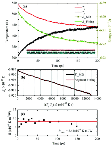 |
| | Fig. 2 (a) Temperature evolution of the individual graphene, phosphorene monolayer, and the total energy change of the graphene monolayer after introducing the thermal impulse. Atomic configuration of the heterostructure in the stable state is shown in the inset. (b) Relationship between the total energy of graphene and the temperature difference (Tg − Tp) integration with time. (c) Segment interfacial thermal resistance values obtained in (b). | |
Table 1 A summary of the interfacial thermal resistances of popular 2D material interfaces, computed from classical MD simulations
| References |
Materials |
Temperature (K) |
R (×10−8 K m2 W−1) |
| Zhang et al.29 |
Graphene/Si |
300 |
3.1–4.9 |
| Li et al.52 |
Graphene/SiC |
300 |
0.091–5.6 |
| Wang et al.53 |
Graphene/SiC |
300–600 |
∼1.03–1.75 |
| Hong et al.30 |
Graphene/copper |
300 |
2.1–3.6 |
| Chang et al.54 |
Graphene/copper/nickel |
230–430 |
∼0.2–0.83 |
| Luo et al.55 |
Graphene/polymer |
298 |
∼1.7 |
| Liu et al.32 |
Graphene/silicene |
200–700 |
∼4.2–16.8 |
| Zhang et al.34 |
Graphene/h-BN |
200–700 |
9.04–29.6 |
| Liu et al.33 |
Graphene/MoS2 |
200–500 |
∼8.3–25 |
| Park et al.56 |
Graphene/CNT |
10–600 |
∼0.018–0.045 |
| Wei et al.57 |
Graphene/graphene |
400–1200 |
∼0.021–0.025 |
| Zhang et al.58 |
Silicene/Si/SiO2 |
100–400 |
1.19–2.49 |
To have a better understanding of the interfacial thermal resistance of the heterostructure, the phonon density of states (PDOS) for both graphene and phosphorene are computed. The PDOS can be calculated by taking the Fourier transform of the velocity autocorrelation function (VACF)
| |  | (3) |
where
Z(
t) = 〈
ν(0)·
ν(t)〉/〈
ν(0)·
ν(0)〉. A higher value of PDOS means that a phonon occupies more states with frequency
ω, while zero PDOS means no phonon with frequency
ω exists in the system. The phonon-power-spectrum analysis provides a quantitative way to assess the power carried by phonons in a system. The overall PDOS of graphene and phosphorene are depicted in
Fig. 3(a). Due to the intrinsic anisotropic phonon properties of graphene, the decomposed PDOS in lateral and out-of-plane directions are calculated separately and the results are shown in
Fig. 3(b) and (c). Thermal resistance is caused by the PDOS mismatch in graphene and phosphorene. Also, unlike graphene, the PDOS of phosphorene are isotropic in all directions and only appear in low frequency regions, which is the reason why phosphorene's thermal conductivity is lower than that of graphene.
10
 |
| | Fig. 3 Phonon-power spectra of phosphorene and graphene. (a), (b), (c) denote the overall, lateral xy directions, and out-of-plane z direction PDOS, respectively. Integration area of each profile is normalized to unity for comparison. | |
3.1 Effects of temperature and contact pressure
Thermal interface materials embedded in FETs or other nano-devices are often placed under different working temperatures. The accumulation of thermal energies in these confined spaces could lead to possible structural failures. Besides, the condensed arrangement of thermal interface materials in layered structures can cause contact pressure variations and then affect the thermal transport efficiency. Thus, to effectively reduce the thermal contact resistance between graphene and phosphorene, the effects of temperature and contact pressure on R are investigated.
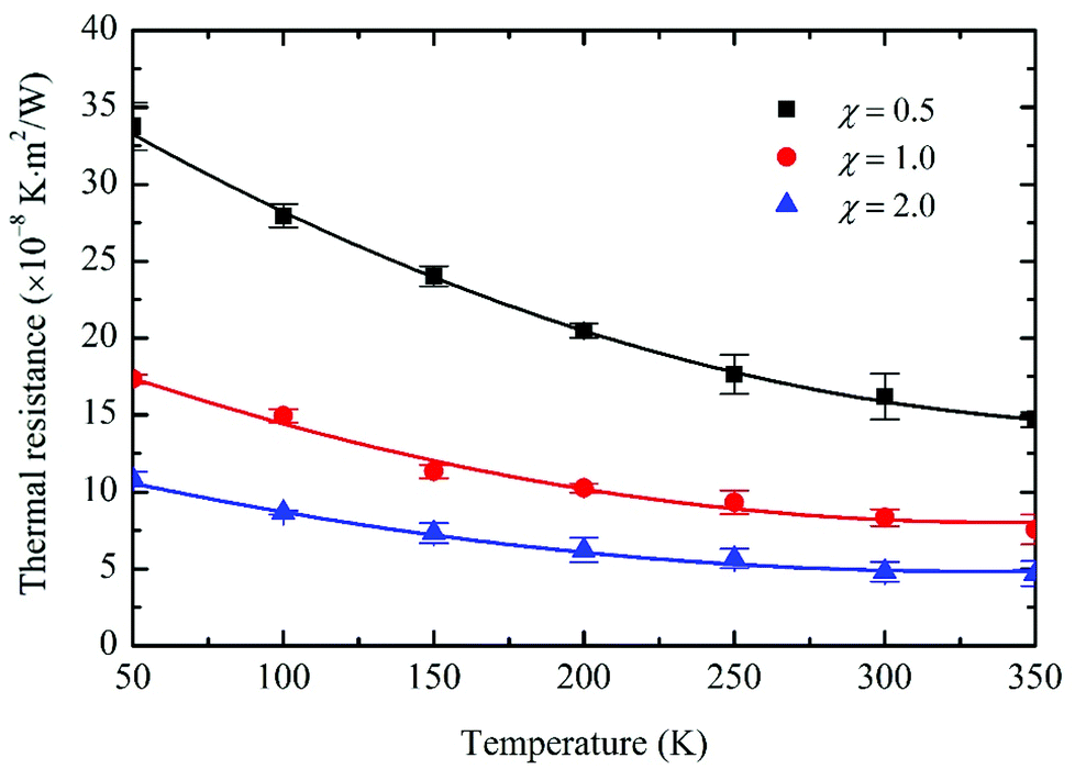
To be consistent with previous computations, the system configuration and simulation setup remain unchanged. Initial equilibrium temperatures varied from 50 K to 350 K. Coupling strength χ is set to 0.5, 1.0 and 2.0 for each temperature value. Five independent simulations are performed for each case to obtain an accurate statistical average of R, as presented in Fig. 4. It is seen that the predicted R values decrease monotonically with temperature. For the χ = 1.0 case, R is reduced by 56.5% from 17.34 × 10⁻⁸ K m2 W−1 to 7.55 × 10⁻⁸ K m2 W−1. As the temperature increases, more phonons with a higher frequency become active in both graphene and phosphorene, which results in higher phonon populations and directly facilitates the thermal transport across the vdW interface. Besides, the more intensive three-phonon scattering at higher temperatures can scatter the high frequency phonons within graphene into various low frequency branches, leading to the higher phonon transmission coefficients and enhanced phonon couplings between graphene and phosphorene. The heat capacities of phosphorene and graphene are functions of temperature and can increase with temperature since more phonon modes would be excited, and as a result, would lead to enhanced interfacial thermal conductance and reduced thermal resistance. In this work, the heat capacities are not directly involved in the thermal resistance calculations since R is determined from temperature and energy correlations. Aside from the heat capacity effects, another important factor that contributes to the reduced thermal resistance is the increased inelastic phonon scattering at the interface and at higher temperatures. The interfacial thermal resistance computed based on the conventional acoustic mismatch model and the diffuse mismatch model is independent of temperature within the classical high temperature limit. This is because the only temperature-dependent parts for both models are the distribution functions, whereas inelastic scattering is not considered at the interfaces. The transient method applied in this work accounts for both elastic and inelastic scatterings at the interface. It has been proven that at van der Waals heterojunctions, inelastic scattering provides the major contribution to the energy transport, surpassing that of the elastic scattering at high temperatures.25 The increase in the probability of inelastic scattering is due to the fact that, at high temperatures, the high frequency phonons might break down into large volumes of low frequency phonons. These low frequency phonons have a higher probability of getting transferred through an interface when compared to the high frequency phonons, leading to higher phonon transmission coefficients and a reduction in the overall interfacial thermal resistance for the system with increasing temperature.
 |
| | Fig. 4 Dependence of the interfacial thermal resistance on the temperature and coupling strength. The predicted R decreases monotonically with temperature and the contact pressure. Each data point is averaged over five independent simulation runs. | |
When the coupling strength χ increases from 0.5 to 2, the predicted thermal resistance decreases by roughly the same ratio of 70.4% at all temperature values. For example, at 300 K, R reduces from 16.2 × 10⁻⁸ K m2 W−1 to 4.8 × 10⁻⁸ K m2 W−1 when χ varies from 0.5 to 2. The R-decreasing trend coincides well with previous studies of SiO2/Si![[thin space (1/6-em)]](https://www.rsc.org/images/entities/char_2009.gif) 35 and silicene/SiO210 interfaces. The enhancement of thermal transport across the interface mainly comes from two aspects. First, the increase in χ enhances the contact pressure, which directly strengthens the graphene/phosphorene phonon coupling, and reduces the thermal resistance. Second, the P atoms in phosphorene act as scattering centers of graphene. The enhanced coupling strength at the interface makes graphene's intrinsic coupling between lateral and out-of-plane phonons stronger, which indirectly facilitates the thermal dissipation.
35 and silicene/SiO210 interfaces. The enhancement of thermal transport across the interface mainly comes from two aspects. First, the increase in χ enhances the contact pressure, which directly strengthens the graphene/phosphorene phonon coupling, and reduces the thermal resistance. Second, the P atoms in phosphorene act as scattering centers of graphene. The enhanced coupling strength at the interface makes graphene's intrinsic coupling between lateral and out-of-plane phonons stronger, which indirectly facilitates the thermal dissipation.
3.2 Effects of vacancy defects
The exceptional mechanical, electrical, and thermal properties of graphene can be attributed to its unique sp2 covalent bonds between carbon atoms.36 However, some defects are still inevitable during the fabrication of graphene sheets.37–39 The structural defects can significantly affect the chemical, electronic and magnetic properties of graphene.40–42 However, the effect of surface defects on interfacial thermal transport, especially for bilayer vdW structures, has not been reported in the literature.
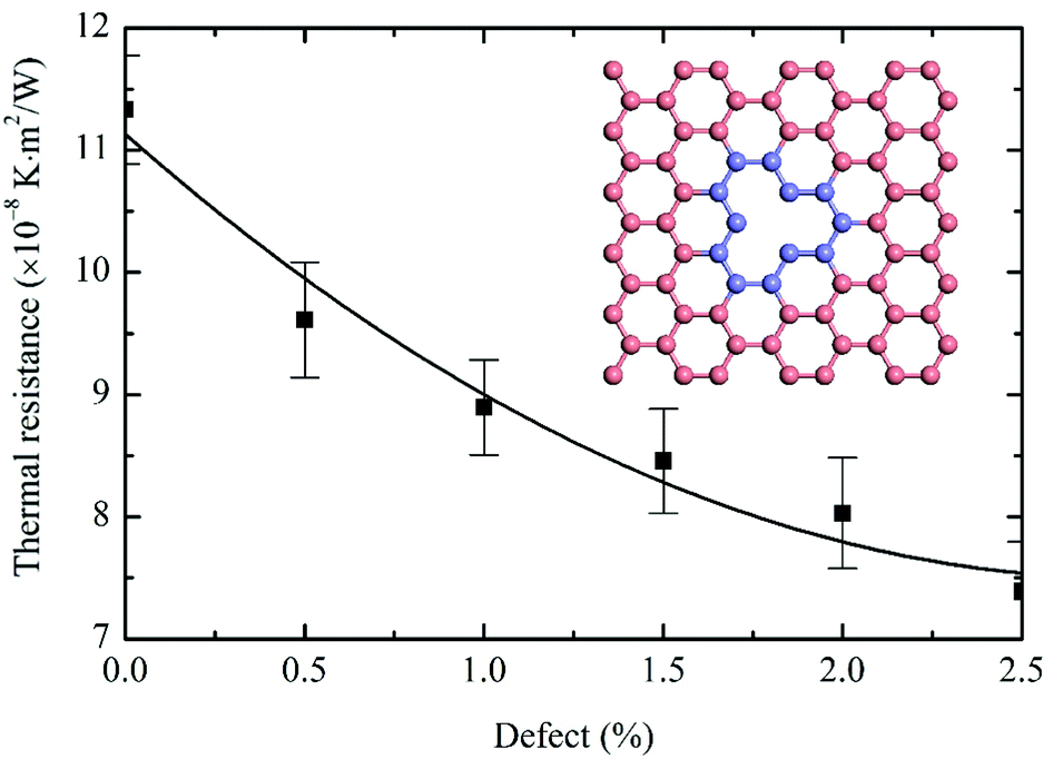
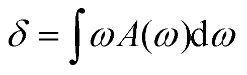
Here, randomly distributed single-vacancy defects (inset of Fig. 5) are created on the graphene monolayer with a 0.5% to 2.5% fraction of the defects. Fig. 5 shows that the predicted thermal resistance R decreases monotonically on increasing the fraction of the defects. A 34.8% R reduction is seen when the fraction of defects increases from 0 to 2.5%. The enhanced lateral and out-of-plane phonon (ZA) coupling in graphene is the major source of interfacial thermal transport. The phonon coupling between in-plane transverse (TA) and longitudinal phonons (LA) is proven to be much faster than those between TA/LA ↔ ZA phonons. Based on the dynamic excitation theory, the phonon-coupling time between TA/LA ↔ ZA is 4.7 times longer than that between TA ↔ LA.43 Since the kinetic energies are evenly distributed among all directions during the heating process, two thirds of the thermal energies are confined in the lateral directions after introducing the thermal impulse. The energy flow rates from the in-plane to out-of-plane phonons can be strengthened by introducing defects into the graphene monolayer, thereby promoting the reduction of interfacial thermal resistance between graphene and phosphorene. To quantitatively confirm this point, the phonon power spectra of pristine and 2.5% defect-containing graphene are computed, and the lateral/flexural PDOS are presented separately in Fig. 6. The overlap areas can be calculated as  , where A(ω) represents the intersection area at frequency ω. The calculated δ for pristine graphene equals 0.348, whereas δ increases to 0.390 for 2.5% defect-containing graphene. The increased overlap areas indicate better couplings between in-plane and out-of-plane phonons in defective graphene, which indirectly enhances the interfacial thermal transport.
 |
| | Fig. 5 Variations of thermal resistance with the fraction of defects in graphene. The calculated R decreases with the defect fraction due to the enhanced phonon coupling within the graphene monolayer. Each data point is averaged over five independent simulation runs. Pink spheres in the inset represent general carbon atoms; blue spheres denote carbon atoms around the single-vacancy defect. | |
 |
| | Fig. 6 Lateral and flexural phonon power spectra of graphene at (a) 0% defect and (b) 2.5% defect levels. The overlap areas become larger at a higher defect level, indicating the enhanced phonon coupling between in-plane and out-of-plane phonons in graphene. | |
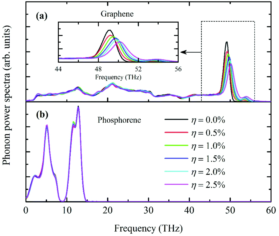
To further explain the decreasing trend of R on increasing the fraction of defects, phonon-power spectra for both graphene and phosphorene under different defect levels are calculated and presented in Fig. 7. The PDOS of phosphorene remain unchanged in all cases, indicating that the defects in graphene barely affect phosphorene. For graphene, the high-frequency G-band phonons exhibit a significant blue-shift on increasing the defect levels. The calculation results are consistent with previous studies.44–46 This frequency blue-shift is an outcome of the strong anharmonic phonon–phonon coupling in MD simulations, demonstrating that the single-vacancy defect improves the energy exchange between in-plane LA/TA phonons and out-of-plane ZA phonons.
 |
| | Fig. 7 Phonon-power spectra of (a) graphene and (b) phosphorene at different defect levels. The PDOS of phosphorene remains unchanged in all cases. The in-plane high frequency phonons in graphene are flattened and a significant blue-shift is observed. The integration area of each profile is normalized to unity for comparison. | |
Due to the isotopic phonon power spectra in phosphorene, it can be speculated that defects in phosphorene would have less effect on the predicted interfacial thermal resistance compared to graphene. Unlike graphene, the lateral and flexural phonons in phosphorene are well mixed in the crystalline structures. To validate this presumption, additional simulations are performed with a low defect ratio of 0.5% in phosphorene at temperature 150 K. The calculation result averaged over 5 independent simulations is 11.49 × 10⁻⁸ K m2 W−1, very close to the zero-defect value of 11.33 × 10⁻⁸ K m2 W−1. However, for the same defect ratio of 0.5% in graphene, the interfacial thermal resistance is reduced to 9.61 × 10⁻⁸ K m2 W−1, about 15.2% lower than the zero-defect result.
3.3 Effects of hydrogenation
Chemical functionalization is an effective approach to modify the thermal, chemical, and mechanical properties of graphene. The fracture strain, shear modulus and shear strength of graphene can be reduced as much as 50% with the hydrogen coverage at 30%.47 Other mechanical properties remain insensitive to hydrogen coverage. It has been found that both the concentration and configuration of hydrogen functional groups have significant influence on the thermal conductivity. By adjusting the coverage and distribution patterns of hydrogen adsorbates on graphene's edge or surface, significant thermal rectifications can be achieved.48–50 Due to the significant effects of hydrogenation on thermal transport, it is necessary to investigate its impact on the interfacial thermal conductance between phosphorene and graphene.
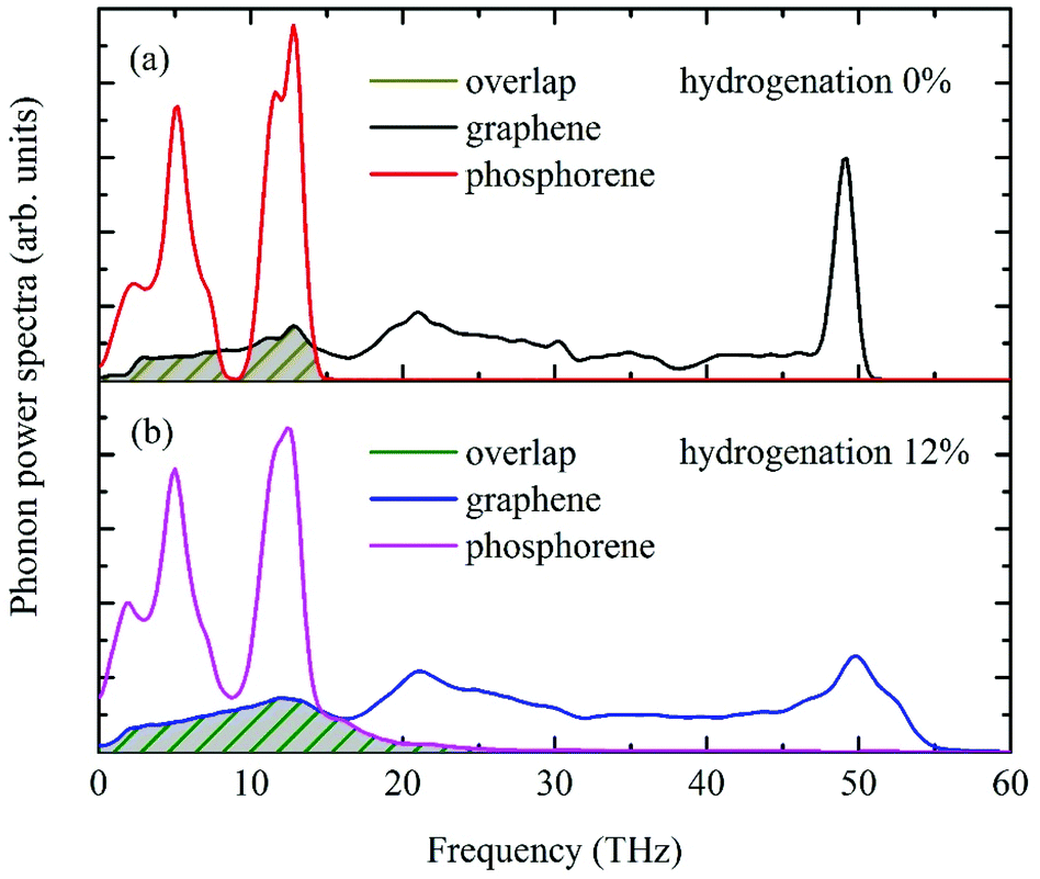
In practice, hydrogen atoms can be attached to the single or both sides of a graphene sheet. Therefore, all three cases, i.e. H-top (graphene is between H atoms and phosphorene), H-bottom (H atoms between graphene and phosphorene) and H-both (H atoms on both sides of graphene), are considered in this work with the coverage ranging from 0% to 12%, while the pattern is random. Atomic configurations of the hydrogenated graphene monolayer are depicted in Fig. 8(a)–(c). Note that for the H-both structure, the total number of hydrogen atoms from both sides equals to those of H-top/H-bottom from one side at the same coverage ratio. As shown in Fig. 8(d), the predicted interfacial thermal resistance R decreases monotonically with the hydrogen coverage. The minimum R occurs when hydrogen atoms are added to the bottom of graphene, i.e., sandwiched between graphene and phosphorene. In this case, the maximum R reduction of 84.5% is observed at 12% hydrogen coverage. When H atoms are directly in contact with P atoms in phosphorene, the phonon coupling between the two sheets is much stronger than other cases, and it offsets the enlarged distances between graphene and phosphorene. The enhanced thermal transport can be attributed to two main factors. First, the extra phonon coupling between H and P atoms directly facilitates the thermal transport at the interface. Compared to the individual graphene monolayer, an extra H–P heat dissipation channel is created in addition to that between C–P atoms. Contributions from this new heat dissipation channel can enhance the surface phonon coupling and reduce the interfacial thermal resistance. Second, the hydrogenation can be treated as surface modification to graphene, which bears similar effects as single-vacancy defect. The absorbed H atoms on graphene can also behave as scattering centers, thereby enhancing the graphene's lateral to flexural direction phonon coupling which indirectly strengthens the thermal transmission from graphene to phosphorene. The enhanced phonon couplings between graphene and phosphorene with hydrogenation can be further proven by the phonon power spectrum analyses. The H-bottom structure is selected for the PDOS computation, and the phonon power spectra of pristine graphene/phosphorene and 12% hydrogen doped graphene/phosphorene are shown in Fig. 9. It is seen that at the 12% hydrogenation level, both the PDOS of graphene and phosphorene are broadened and a larger overlap is observed, indicating the enhanced phonon interactions between graphene and phosphorene.
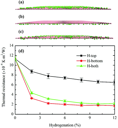 |
| | Fig. 8 Atomic configurations of (a) H-top, (b) H-bottom and (c) H-both hydrogenation types. Pink layers represent graphene; green spheres denote adsorbed hydrogen atoms. (d) Effect of hydrogenation on the interfacial thermal transport between phosphorene and graphene. The predicted R decreases monotonically with hydrogenation coverage. Each data point is averaged over five independent simulation runs. | |
 |
| | Fig. 9 Phonon power spectra of graphene and phosphorene at (a) 0% and (b) 12% hydrogenation levels. The overlap areas increase with a higher hydrogenation ratio, indicating the enhanced phonon couplings between graphene and phosphorene. | |
Although the interfacial thermal resistance between graphene and phosphorene can be reduced by hydrogen functionalization, the quantitative contributions of H and C atoms to the thermal transport are still open questions. The effects of H atoms on the enhanced thermal transport can be understood by turning off the interactions between C–P atoms or H–P atoms. Since minimum R occurs when H atoms reside in the middle of graphene and phosphorene, the H-bottom configuration is used in the following calculations. The LJ parameters εC–P and εH–P are set to zero separately; the calculated R values are summarized in Fig. 10. R reaches the lowest level when both C and H atoms are involved (εC–P ≠ 0, εH–P ≠ 0) in the thermal transport. When only H atoms are involved (εC–P = 0, εH–P ≠ 0), R increases significantly by two orders of magnitude. R values with only C atoms involved (εC–P ≠ 0, εH–P = 0) are in between the two cases. The calculation results indicate that the thermal transport is still dominated by C–P interactions even with the hydrogenation. Interfacial thermal resistance is mostly dependent on the materials’ atomic mass ratio at the interface. The predicted R value increases monotonically with the atomic mass ratio, which further explains the greater contributions from carbon atoms since the P/H mass ratio is 12 times higher than that of P/C.51
 |
| | Fig. 10 A comparison of the interfacial thermal resistance with contributions from only C atoms and H atoms. The predicted R has the lowest values when both C and H atoms are involved in the thermal transport, while it has significantly higher values when only H atoms contribute to the thermal transport. | |
4. Conclusion
Inter-plane thermal conductance at the phosphorene–graphene vdW interface is investigated using classical MD simulations. Several modulators such as system temperature, contact pressure, vacancy defect, and hydrogenation are explored, with which significant thermal resistance reductions are observed. The maximum R reduction is predicted as 84.5% when the hydrogenation is applied on the near-phosphorene-side graphene surface. Other factors such as temperature, coupling strength, and fraction of single-vacancy defects have relatively weaker influences on R, which decrease R values by 56.5%, 70.4%, and 34.8%, respectively. The PDOS mismatch in graphene and phosphorene appears to be the key factor for the thermal resistance. Note that unlike graphene, the PDOS of phosphorene are isotropic in all directions and only exist in the low-frequency region. Reductions of R at the interface can be attributed to several factors, including increased phonon population, enhanced anharmonic phonon scattering at higher temperatures, as well as strengthened coupling between lateral and out-of-plane phonons of graphene with increasing fraction of the defect or functionalization. Note also that the interfacial thermal resistance between phosphorene–graphene is less than that of other 2D bilayer heterostructures, a distinct advantage for practical applications. Our study provides new insights into thermal resistance in the phosphorene–graphene bilayer, which can be useful for the better design of heterostructures for nanoelectronic applications.
Acknowledgements
Support from the Nebraska Center for Energy Sciences Research and the Holland Computing Center at the University of Nebraska-Lincoln is greatly appreciated.
References
- J. Zhang, F. Xu, Y. Hong, Q. Xiong and J. Pan, RSC Adv., 2015, 5, 89415–89426 RSC.
- J. Zhang, X. Wang and H. Xie, Phys. Lett. A, 2013, 377, 2970–2978 CrossRef CAS.
- J. Zhang, X. Huang, Y. Yue, J. Wang and X. Wang, Phys. Rev. B: Condens. Matter, 2011, 84, 235416 CrossRef.
- S. Ghosh, I. Calizo, D. Teweldebrhan, E. P. Pokatilov, D. L. Nika, A. A. Balandin, W. Bao, F. Miao and C. N. Lau, Appl. Phys. Lett., 2008, 92, 151911 CrossRef.
- M. Y. Liao and Y. Koide, Crit. Rev. Solid State Sci., 2011, 36, 66–101 CrossRef CAS.
- T. Shimizu, J. Haruyama, D. C. Marcano, D. V. Kosinkin, J. M. Tour, K. Hirose and K. Suenaga, Nat. Nanotechnol., 2011, 6, 45–50 CrossRef CAS PubMed.
- S. J. Zhang, S. S. Lin, X. Q. Li, X. Y. Liu, H. A. Wu, W. L. Xu, P. Wang, Z. Q. Wu, H. K. Zhong and Z. J. Xu, Nanoscale, 2016, 8, 226–232 RSC.
- S. J. Han, K. A. Jenkins, A. V. Garcia, A. D. Franklin, A. A. Bol and W. Haensch, Nano Lett., 2011, 11, 3690–3693 CrossRef CAS PubMed.
- J. Qiao, X. Kong, Z.-X. Hu, F. Yang and W. Ji, Nat. Commun., 2014, 5, 4475 CAS.
-
(a) Y. Hong, J. Zhang, X. Huang and X. C. Zeng, Nanoscale, 2015, 7, 18716–18724 RSC;
(b) Y. Hong, J. Zhang and X. C. Zeng, J. Phys. Chem. C, 2016 DOI:10.1021/acs.jpcc.6b07262.
- J. Dai and X. C. Zeng, RSC Adv., 2014, 4, 48017–48021 RSC.
- H. Guo, N. Lu, J. Dai, X. Wu and X. C. Zeng, J. Phys. Chem. C, 2014, 118, 14051–14059 CAS.
- L. Li, Y. Yu, G. J. Ye, Q. Ge, X. Ou, H. Wu, D. Feng, X. H. Chen and Y. Zhang, Nat Nanotechnol., 2014, 9, 372–377 CrossRef CAS PubMed.
- K. S. Novoselov, A. Mishchenko, A. Carvalho and A. H. Castro Neto, Science, 2016, 353, aac9439 CrossRef CAS PubMed.
- J. E. Padilha, A. Fazzio and A. J. R. da Silva, Phys. Rev. Lett., 2015, 114, 066803 CrossRef CAS PubMed.
- A. Hashmi, U. Farooq and J. Hong, Curr. Appl. Phys., 2016, 16, 318–323 CrossRef.
- Y. Cai, G. Zhang and Y.-W. Zhang, winword, 2015, 119, 13929–13936 CAS.
- S. Plimpton, J. Comput. Phys., 1995, 117, 1–19 CrossRef CAS.
- W. B. Donald, A. S. Olga, A. H. Judith, J. S. Steven, N. Boris and B. S. Susan, J. Phys.: Condens. Matter, 2002, 14, 783 CrossRef.
- J. Jin-Wu, Nanotechnology, 2015, 26, 315706 CrossRef PubMed.
- M. Daniel, H. L. Caio and C. Alexander, 2D Mater., 2016, 3, 011005 CrossRef.
- C. Kun, W. Jing, W. Ning, C. Haifang and Q. Qing-Hua, Nanotechnology, 2016, 27, 235703 CrossRef PubMed.
- L. Xiangbiao, H. Feng, X. Hang and C. Xi, Nanotechnology, 2016, 27, 215701 CrossRef PubMed.
- A. K. Rappe, C. J. Casewit, K. S. Colwell, W. A. Goddard and W. M. Skiff, J. Am. Chem. Soc., 1992, 114, 10024–10035 CrossRef CAS.
- R. J. Stevens, L. V. Zhigilei and P. M. Norris, Int. J. Heat Mass Tranfer., 2007, 50, 3977–3989 CrossRef.
- S. Yu, S. Yang and M. Cho, J. Appl. Phys., 2011, 110, 124302 CrossRef.
- K. Gordiz and A. Henry, New J. Phys., 2015, 17, 103002 CrossRef.
- P. E. Hopkins and P. M. Norris, Appl. Phys. Lett., 2006, 89, 131909 CrossRef.
- J. Zhang, Y. Wang and X. Wang, Nanoscale, 2013, 5, 11598–11603 RSC.
- Y. Hong, L. Li, X. C. Zeng and J. Zhang, Nanoscale, 2015, 7, 6286–6294 RSC.
- X. Zhiping and J. B. Markus, J. Phys.: Condens. Matter, 2012, 24, 475305 CrossRef PubMed.
- B. Liu, J. A. Baimova, C. D. Reddy, A. W.-K. Law, S. V. Dmitriev, H. Wu and K. Zhou, ACS Appl. Mater. Interfaces, 2014, 6, 18180–18188 CAS.
- B. Liu, F. Meng, C. D. Reddy, J. A. Baimova, N. Srikanth, S. V. Dmitriev and K. Zhou, RSC Adv., 2015, 5, 29193–29200 RSC.
- J. Zhang, Y. Hong and Y. Yue, J. Appl. Phys., 2015, 117, 134307 CrossRef.
- J. Chen, G. Zhang and B. Li, J. Appl. Phys., 2012, 112, 064319 CrossRef.
- A. K. Geim and K. S. Novoselov, Nat. Mater., 2007, 6, 183–191 CrossRef CAS PubMed.
- A. M. Dimiev, G. Ceriotti, A. Metzger, N. D. Kim and J. M. Tour, ACS Nano, 2016, 10, 274–279 CrossRef CAS PubMed.
- J. S. Lee, S. I. Kim, J. C. Yoon and J. H. Jang, ACS Nano, 2013, 7, 6047–6055 CrossRef CAS PubMed.
- J. H. Lee, D. W. Shin, V. G. Makotchenko, A. S. Nazarov, V. E. Fedorov, Y. H. Kim, J. Y. Choi, J. M. Kim and J. B. Yoo, Adv. Mater., 2009, 21, 4383–4387 CrossRef CAS PubMed.
- D. W. Boukhvalov and M. I. Katsnelson, Nano Lett., 2008, 8, 4373–4379 CrossRef CAS PubMed.
- G. M. Rutter, J. N. Crain, N. P. Guisinger, T. Li, P. N. First and J. A. Stroscio, Science, 2007, 317, 219–222 CrossRef CAS PubMed.
- M. Sepioni, R. R. Nair, S. Rablen, J. Narayanan, F. Tuna, R. Winpenny, A. K. Geim and I. V. Grigorieva, Phys. Rev. Lett., 2010, 105, 207205 CrossRef CAS PubMed.
- J. Zhang, X. Wang and H. Xie, Phys. Lett. A, 2013, 377, 721–726 CrossRef CAS.
- D. Liu, P. Yang, X. Yuan, J. Guo and N. Liao, Phys. Lett. A, 2015, 379, 810–814 CrossRef CAS.
- Y. L. Yang and Y. Lu, Chin. Phys. B, 2014, 23, 106501 CrossRef.
- P. Anees, M. C. Valsakumar and B. K. Panigrahi, 2D Mater., 2015, 2, 035014 CrossRef.
- A. Hadizadeh Kheirkhah, E. Saeivar Iranizad, M. Raeisi and A. Rajabpour, Solid State Commun., 2014, 177, 98–102 CrossRef CAS.
- H. Fan, L. Deng, X. Yuan, J. Guo, X. Li and P. Yang, RSC Adv., 2015, 5, 38001–38005 RSC.
- Y. Tang, J. Li, X. Wu, Q. Liu, Y. Liu and P. Yang, Appl. Surf. Sci., 2016, 362, 86–92 CrossRef CAS.
- C. Melis, G. Barbarino and L. Colombo, Phys. Rev. B: Condens. Matter, 2015, 92, 245408 CrossRef.
- S. Wang and X. Liang, Int. J. Thermophys., 2010, 31, 1935–1944 CrossRef CAS.
- M. Li, J. Zhang, X. Hu and Y. Yue, Appl. Phys. A: Mater. Sci. Process., 2015, 119, 415–424 CrossRef CAS.
- H. Wang, J. Gong, Y. Pei and Z. Xu, ACS Appl. Mater. Interfaces, 2013, 5, 2599–2603 CAS.
- S.-W. Chang, A. Nair and M. Buehler, J. Phys.: Condens. Matter, 2012, 24, 245301 CrossRef PubMed.
- T. Luo and J. R. Lloyd, Adv. Funct. Mater., 2012, 22, 2495–2502 CrossRef CAS.
- J. Park and V. Prakash, J. Appl. Phys., 2014, 116, 014303 CrossRef.
- Z. Wei, Z. Ni, K. Bi, M. Chen and Y. Chen, Phys. Lett. A, 2011, 375, 1195–1199 CrossRef CAS.
- J. Zhang, Y. Hong, Z. Tong, Z. Xiao, H. Bao and Y. Yue, Phys. Chem. Chem. Phys., 2015, 17, 23704–23710 RSC.
|
| This journal is © The Royal Society of Chemistry 2016 |
Click here to see how this site uses Cookies. View our privacy policy here. 
 Open Access Article
 This Open Access Article is licensed under a Creative Commons Attribution-Non Commercial 3.0 Unported Licence
 a,
Jingchao
Zhang
*b and
Xiao Cheng
Zeng
*a
a,
Jingchao
Zhang
*b and
Xiao Cheng
Zeng
*a


 , where E0 is the initial energy. The computed interfacial thermal resistance at 300 K is 8.41 × 10⁻⁸ K m2 W−1, which is in the same order of magnitude as other vdW bilayer structures.32–34 A summary of thermal resistances within common 2D material interfaces is presented in Table 1. From these data, we can conclude that R between graphene and phosphorene is higher than that between graphene and metal/polymer substrates, but is lower than graphene/silicene, graphene/h-BN and graphene/MoS2 bilayer structures. The temporal evolution of R is shown in Fig. 2(b). Since the energy decay is driven by the temperature difference ΔT = (Tg − Tp) as shown in Fig. 2(a), the phosphorene energy changes against
  are plotted. It is seen that the Et profile has a linear relationship with
  . The Et profile is divided into many segments as shown in Fig. 2(b). For each segment (t1 to t2), R can be treated as a constant, and can be determined by a linear fitting of the curve. The fitted slope equals A/R, and can be used to determine R. As presented in Fig. 2(c), the calculated instant R values vary slightly around the overall fitting results, indicating that the thermal resistance is constant during the transient process.


 , where A(ω) represents the intersection area at frequency ω. The calculated δ for pristine graphene equals 0.348, whereas δ increases to 0.390 for 2.5% defect-containing graphene. The increased overlap areas indicate better couplings between in-plane and out-of-plane phonons in defective graphene, which indirectly enhances the interfacial thermal transport.