
 Open Access Article
 This Open Access Article is licensed under a
 Creative Commons Attribution 3.0 Unported Licence
Tunable doping of graphene by using physisorbed self-assembled networks†
Roald
Phillipson
a,
César J.
Lockhart de la Rosa
bc,
Joan
Teyssandier
a,
Peter
Walke
a,
Deepali
Waghray
a,
Yasuhiko
Fujita
a,
Jinne
Adisoejoso
a,
Kunal S.
Mali
a,
Inge
Asselberghs
c,
Cedric
Huyghebaert
c,
Hiroshi
Uji-i
ad,
Stefan
De Gendt
*ce and
Steven
De Feyter
 *a
*a
aKU Leuven-University of Leuven, Department of Chemistry, Division of Molecular Imaging and Photonics, Celestijnenlaan 200F, B-3001 Leuven, Belgium. E-mail: steven.defeyter@kuleuven.be
bKU Leuven, Department of Metallurgy and Materials Engineering, Kasteelpark Arenberg 44, B-3001 Leuven, Belgium
cimec, Kapeldreef 75, B-3001 Leuven, Belgium. E-mail: Stefan.DeGendt@imec.be
dRIES, Hokkaido University, Sapporo, 001-0020, Japan
eKU Leuven-University of Leuven, Department of Chemistry, Division of Molecular Design and Synthesis, Celestijnenlaan 200F, B-3001 Leuven, Belgium
First published on 24th November 2016
Abstract
One current key challenge in graphene research is to tune its charge carrier concentration, i.e., p- and n-type doping of graphene. An attractive approach in this respect is offered by controlled doping via well-ordered self-assembled networks physisorbed on the graphene surface. We report on tunable n-type doping of graphene using self-assembled networks of alkyl-amines that have varying chain lengths. The doping magnitude is modulated by controlling the density of the strong n-type doping amine groups on the surface. As revealed by scanning tunneling and atomic force microscopy, this density is governed by the length of the alkyl chain which acts as a spacer within the self-assembled network. The modulation of the doping magnitude depending on the chain length was demonstrated using Raman spectroscopy and electrical measurements on graphene field effect devices. This supramolecular functionalization approach offers new possibilities for controlling the properties of graphene and other two-dimensional materials at the nanoscale.
Introduction
Since its first isolation in 2004, graphene, a single atom thick layer of sp2-hybridized carbon, has attracted enormous interest from the scientific community and a myriad of applications have been envisioned.1,2 In particular its outstanding physical and electrical properties make it a relevant material for integration in electronic applications, e.g., as channels or interconnects in field-effect transistors (FETs) and as transparent electrodes in optoelectronic devices.3,4 However, one of the major issues that prevents its introduction into technological applications is that, although graphene has a high charge carrier mobility, its intrinsic conductivity is low due to the negligible charge carrier density near the Dirac point. In addition, many applications require precise engineering of the work function to lower the energy barrier at the interface with semiconducting materials.5 Both these issues can be overcome through p-type or n-type doping.6 Currently, two approaches for doping have been presented based on either substitutional or adsorbate-induced protocols. Replacing carbon atoms within the graphene lattice by nitrogen or boron, indeed causes a shift in the work function, but it also disrupts the graphene lattice in an uncontrollable manner, thereby decreasing the charge carrier mobility.7 Doping using physisorbed adsorbates through charge transfer with graphene, on the other hand, provides an elegant, non-destructive method that preserves the carrier mobility.8 Gas adsorption, alkali atoms and organic molecules have been shown to cause doping of the underlying graphene,9–13 however, the distribution of adsorbates is often inhomogeneous resulting in uncontrolled doping.One of the attractive routes towards controlled functionalization of graphene is via the use of two-dimensional (2D) supramolecular self-assembly of molecular building blocks.14–16 Although self-assembly on graphene has been intensively investigated, the focus has mainly been on fundamental aspects.17–22 Depending on the chemical nature of the building block and interplay of external parameters like solute concentration, solvent choice or temperature, precise control over the molecular organization on the surface can be achieved.23,24 Accordingly, by incorporating dopant moieties within the molecular building block, the underlying graphene can be doped in a uniform and well-controlled manner. P-type doping using self-assembled monolayers of alkylphosphonic acid derivatives and n-type doping using alkylamine derivatives have been demonstrated.25,26 However, demonstration of tunable control over the doping effect by rational design of the self-assembling species has not yet been explored.
In this contribution, we present a robust and reproducible method for tuning the level of n-type doping by controlling the density of amine groups present on the graphene surface. This method is based on the use of aliphatic amines which differ only in the length of the alkyl chain. Within the 2D self-assembled networks, the length of the alkyl chains determines the density of the amine groups at the interface by acting as a spacer, as revealed by scanning tunneling microscopy (STM) and atomic force microscopy (AFM). Tunable n-type doping via modulation of the alkyl chain length was proven using Raman spectroscopy and electrical measurements performed on field-effect transistor (FET) devices. Graphene grown by chemical vapor deposition (CVD) transferred to SiO2 was used as it is the most promising graphene type from a technological viewpoint due its quality and large scale, low cost production.
Experimental
Materials
Octadecylamine (ODA, ≥99%) and toluene (CHROMASOLV®, ≥99.8%) were purchased from Sigma-Aldrich and ethanol (Uvasol®, ≥99.9%) was purchased from Merck KGaA. All chemicals were used without further purification. Synthesis of nonacosylamine (NCA) is described in the ESI.† HOPG (grade ZYB, Advanced Ceramics Inc., Cleveland, OH) substrates were cleaved on both sides before functionalization. For AFM/Raman experiments, 1 × 1 cm2 CVD grown graphene samples on SiO2 (300 nm) were obtained from Graphenea and cleaned prior to use in toluene for 1 h at 80 °C (ESI Fig. S3†).Self-assembled film preparation
HOPG and CVD grown graphene (devices) were functionalized with ODA or NCA via dip coating or drop casting. For dip coating, the samples were immersed for 30 min in the dopant solution and subsequently withdrawn using a computer controlled sample stage which allows for precise control of the speed of withdrawal, which was set at 1 mm min−1. For functionalization with ODA via dip coating, a 10−3 M solution in ethanol was used and for NCA, a 10−4 M solution in ethanol/toluene (50/50 v/v%) was used. Functionalization with ODA and NCA via drop casting was performed using 10−4 M solutions (30 μl) in ethanol and ethanol/toluene (50/50 v/v%), respectively. All procedures were carried out under ambient conditions at room temperature.Scanning probe microscopy
STM experiments were performed using a Molecular Imaging STM (Keysight) system, operating in constant-current mode. STM tips were prepared by mechanical cutting of a Pt/Ir wire (80%/20%, diameter 0.25 mm). The bias voltage refers to the substrate. AFM measurements were performed on a PicoSPM (Keysight) machine under ambient conditions with silicon cantilevers (AC160TS or AC240TS; Olympus). Gwyddion and Scanning Probe Image Processor (SPIP) softwares (Image Metrology ApS) were used for image analysis.Raman characterization
Raman measurements were performed with an OmegaScopeTM 1000 (AIST-NT). Laser light from a He–Ne laser (632.8 nm) was reflected by using a dichroic mirror (Chroma, Z633RDC) and then focused onto the sample surface by using an objective (MITUTOYO, BD Plan Apo 100×, N.A. 0.7). The optical density at the sample surface was about 500 kW cm−2. Raman scattering was collected with the same objective and directed to a Raman spectrograph (Horiba JY, iHR-320) equipped with a cooled charge-coupled device (CCD) camera operating at −100 °C (Andor, DU920P) through the dichroic mirror, a pinhole and a long pass filter (Chroma, HQ645LP). Accumulation time for all spectra was 3 s. Measurements were carried out under ambient conditions and at room temperature.Graphene FET fabrication
For device fabrication, CVD grown graphene already transferred to Si++/SiO2 (90 nm) substrates (Graphenea) was used. After cleaning the samples in acetone and IPA, graphene was patterned using photolithography. For this purpose, first poly(methyl methacrylate) (3%) in chlorobenzene was spun at 6000 rpm as a protective layer for the graphene and then an IX845 resist was spun at 4000 rpm for 30 s and baked for 1 min at 120 °C for photolithography patterning. The samples were then developed in OPD 5262 and stripped with O2 plasma. After the patterning of graphene, the residual resist was removed by immersion in acetone at 50 °C followed by isopropyl alcohol (IPA) dip and N2 blow dry. Then the source and drain were deposited by lift-off using photolithography (IX845 resist). For the metal contact, a 70 nm Pd layer was used. After lift-off, the devices were once more cleaned with acetone, IPA dip and N2 blow dry. For the characterization of the devices a Keithley 4200 parameter analyzer was used with a Cascade probe station in a dark environment and a constant flow of 1 scfm of N2 over the sample.Results and discussion
Two alkyl amines, namely, octadecylamine (ODA) and nonacosylamine (NCA) (Scheme 1) were chosen for demonstrating tunable doping of graphene using self-assembled monolayers. Aliphatic compounds form stable self-assembled patterns with their chains orienting parallel to graphitic surfaces due to commensurability between the alkyl chains and the substrate lattice.27 By varying the length of the alkyl chain (spacer), the periodicity of the self-assembled pattern can be tuned and thereby also tuning the density of the amine groups (dopant moieties), which is inversely proportional to the alkyl chain length. Based on the lengths of the molecules under investigation, (18 carbon atoms for ODA and 29 for NCA) the amine group density on the graphene surface, and thus also the doping effect, is expected to be 1.6 times higher for ODA compared to NCA.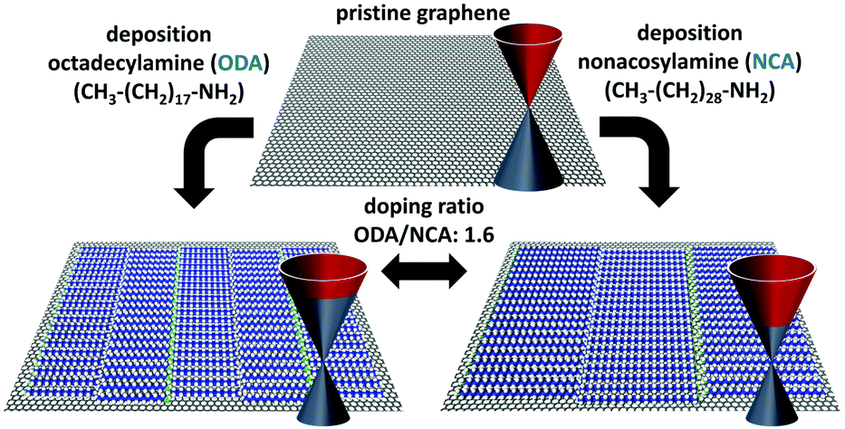 | ||
| Scheme 1 Schematic illustration of the concept of tunable doping by controlling the density of dopant moieties on the surface using self-assembled networks. | ||
Before studying the self-assembly of the two molecules on graphene, the self-assembled networks were first characterized using both STM as well as AFM on highly oriented pyrolytic graphite (HOPG) which served as a model surface. HOPG offers large, atomically flat terraces and thus is a more straightforward platform to study self-assembly. Achieving molecular resolution on CVD grown graphene transferred to SiO2 on the other hand is typically more challenging due to its appreciably higher surface roughness caused due to the underlying SiO2 substrate and also due to contamination from the transfer process.28,29 The choice of HOPG as a model surface for subsequent measurements on graphene is motivated from previous studies, which showed that in general, there is almost no difference between self-assembled structures formed on graphene and HOPG.30,31
To study how the molecules arrange on a graphitic surface, STM was carried out at the 1-phenyloctane/HOPG interface. STM is capable of imaging self-assembled networks with sub-molecular resolution and is therefore a powerful tool to study the precise arrangement of molecules on surfaces. STM measurements were performed by depositing a saturated solution of NCA or ODA in 1-phenyloctane on freshly cleaved HOPG and subsequent imaging under ambient conditions at the solution–solid interface. The high resolution STM image shown in Fig. 1a reveals that ODA is ordered in a lamellar structure characteristic of alkanes. Within the lamella, the molecules are oriented in a head-to-head configuration to facilitate hydrogen bonding between the amine groups, with the alkyl chains perpendicular to the lamella axis. NCA forms similar self-assembled networks as ODA, however, the NCA molecules are randomly orientated within the lamella (head-to-head or tail-to-head, see Fig. 1b). This difference can be explained by the stronger intermolecular and molecule–substrate interactions of the longer alkyl chain, resulting in a kinetically trapped less ordered structure. Based on the periodicity of the lamella, 4.9 ± 0.1 nm for ODA and 4.1 ± 0.1 nm for NCA, and the intermolecular distance within the lamella, 0.47 ± 0.05 nm and 0.43 ± 0.08 nm, respectively, the density of the amine groups on the surface can be estimated to be 0.89 ± 0.03 nm−2 and 0.56 ± 0.01 nm−2. Thus, based on the STM measurements, the amine group density is 1.6 ± 0.1 times higher for ODA compared to NCA, which is in agreement with the ratio of the alkyl chain lengths.
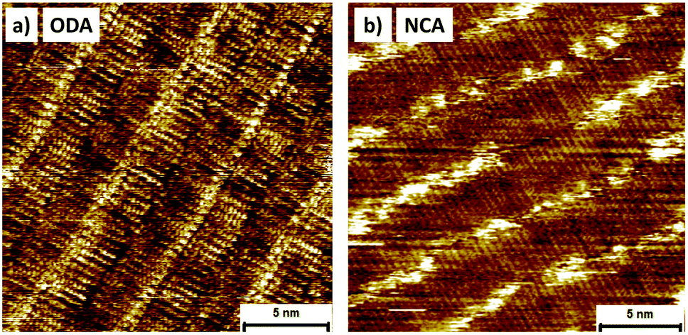 | ||
| Fig. 1 STM characterization of self-assembled networks of ODA and NCA on HOPG. (a) STM image of ODA self-assembled at the 1-phenyloctane/HOPG interface, Iset = 60 pA, Vset = −800 mV. (b) STM image of NCA self-assembled at the 1-phenyloctane/HOPG interface, Iset = 35 pA, Vset = −700 mV. | ||
For doping using self-assembled networks of ODA and NCA, dry uniform films need to be prepared on graphene. In this regard, a deposition protocol for thin, fully surface covering films was first developed on HOPG. To deposit these films, dip coating was used as it results in highly uniform films and to characterize molecular ordering, surface coverage and domain sizes, AFM was employed. Fig. 2a and b show AFM images after dip coating HOPG in ODA and NCA in ethanol and ethanol/toluene (50/50 v/v%) solutions, respectively. Different solvents were used for these compounds due to solubility limitations. In addition, the samples were annealed for 1 minute at 100 °C on a hot plate to improve the film quality and increase domain sizes (ESI Fig. S1 and S2†). The deposition protocol results in self-assembled films with full surface coverage. AFM images reveal that both molecules form lamellar structures similar to those found at the 1-phenyloctane/HOPG interface. The periodicity of the ODA lamella is 5.0 ± 0.3 nm which is in good agreement with the STM measurements on HOPG. For NCA however, the periodicity is 7.8 ± 0.2 nm which indicates that, in contrast to the previously described STM measurements, the molecules are predominately in the thermodynamically favourable head-to-head orientation. This discrepancy between the two measurements can be explained by the different conditions under which the measurements were performed: while STM was performed at the 1-phenyloctane/HOPG interface, AFM was carried out on dry films created by dip coating in toluene/ethanol solution, and followed by annealing. Nonetheless, this difference in organization of individual molecules within the lamella does not change the density of the amine groups on the graphene surface.
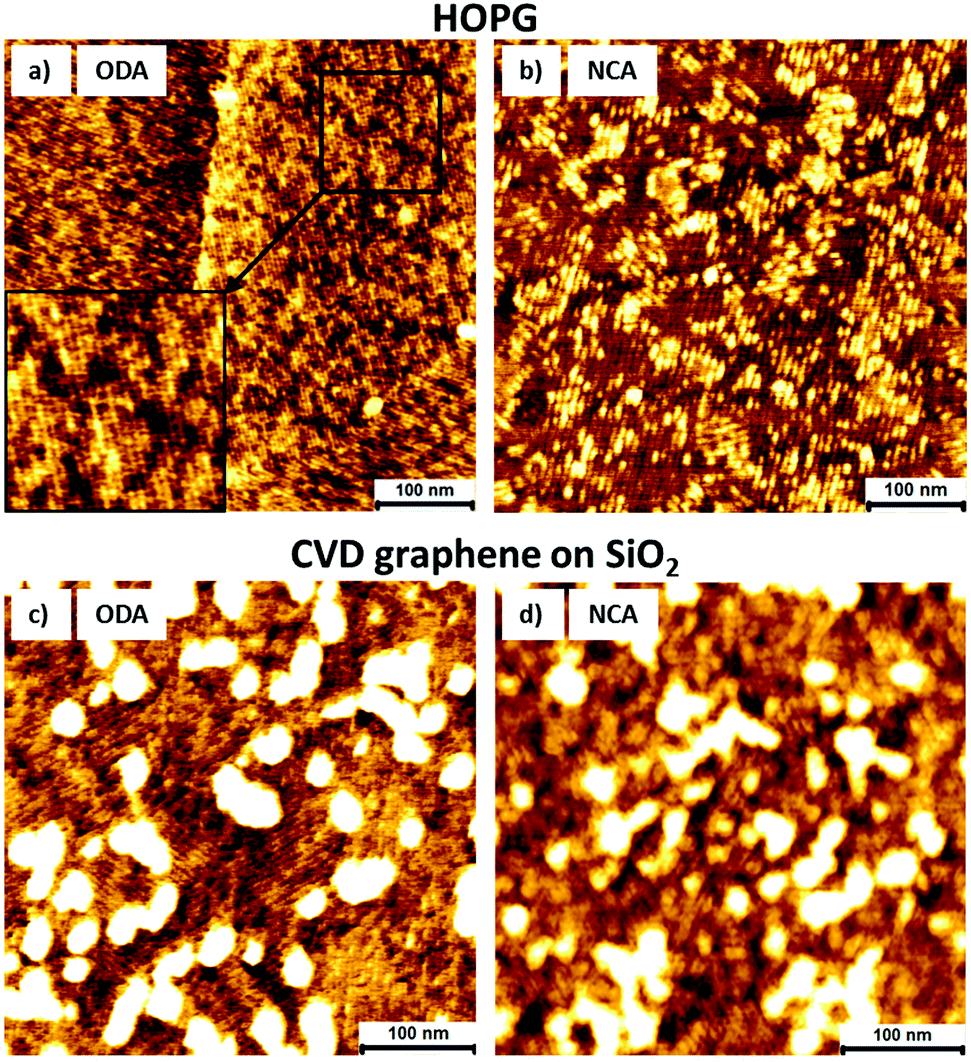 | ||
| Fig. 2 Structural characterization of self-assembled networks of ODA and NCA on HOPG and CVD graphene on SiO2 using AFM. (a) AFM topography image of HOPG functionalized with ODA. (b) AFM topography image of HOPG functionalized with NCA. (c) and (d), AFM topography images of graphene after functionalization with ODA (c) and NCA (d) via dip coating and subsequent annealing. Despite contamination (bright features), the lamellar organization of the compounds can still be visualized. | ||
To functionalize CVD grown graphene on SiO2, the same deposition conditions were used as on HOPG. Fig. 2c and d show AFM images of graphene after deposition of ODA and NCA and subsequent annealing. Despite its high surface roughness, the molecules form similar self-assembled structures on CVD graphene as on HOPG. The alkyl chains are aligned along the graphene symmetry axes and the periodicities of the lamella are 5.3 ± 0.3 nm for ODA and 8.0 ± 0.2 nm for NCA. However, the domain sizes are in general smaller than those on HOPG. These smaller domains are possibly caused by the corrugation of graphene or polymeric contamination originating from the transfer process. The bright features in the images likely correspond to this contamination as they are not present on functionalized HOPG and were present on the graphene surface prior to deposition (ESI Fig. S3†).
In order to compare the doping effect of ODA and NCA, Raman spectroscopy was performed on CVD grown graphene before and after functionalization. Raman spectroscopy is a well-known technique to study various properties of graphene, such as defect density, number of layers and also doping. Upon n- or p-type doping, the G peak position, Pos(G), shifts from its charge neutral position (1581.6 cm−1) to higher wavenumbers. In addition, both types of doping results in a decrease of the ratio of the 2D and G peak intensities, I(2D)/I(G), and the full width at half maximum of the G-peak, FWHM(G).32,33 The behavior of the 2D peak position, Pos(2D), upon doping is more complex. It increases for p-type doping while for n-type doping it first increases slightly followed by a decrease at higher doping levels.32,33Fig. 3a shows typical Raman spectra before and after deposition of ODA and NCA. Pos(G) is located at 1599 cm−1 before deposition, indicating that the graphene sample is heavily p-type doped due to the strong interaction with the SiO2 substrate and doping by oxygen and water from the ambient.34 Upon deposition of ODA or NCA using the same dip coating protocol as used for the AFM characterization described before, Pos(G) shifts to lower wavenumbers due to electron donation from the molecules to graphene, leading to a reduction in p-type doping. The n-type doping ability of amine groups can be attributed to two different mechanisms. First, it has been demonstrated using first principles calculations that orbital mixing between graphene states with molecular states of ammonia results in a small amount of charge transfer.35 However, the large doping effect found experimentally for amine groups cannot be fully attributed to this. A second mechanism that can explain this observation is that polar molecules, like water or ammonia, result in charge transfer due to the formation of a dipole layer.36,37 Based on the larger red shift of Pos(G) and a larger increase of I(2D)/I(G) after deposition of ODA compared to NCA, it is clear that the former has a higher doping effect than the latter.
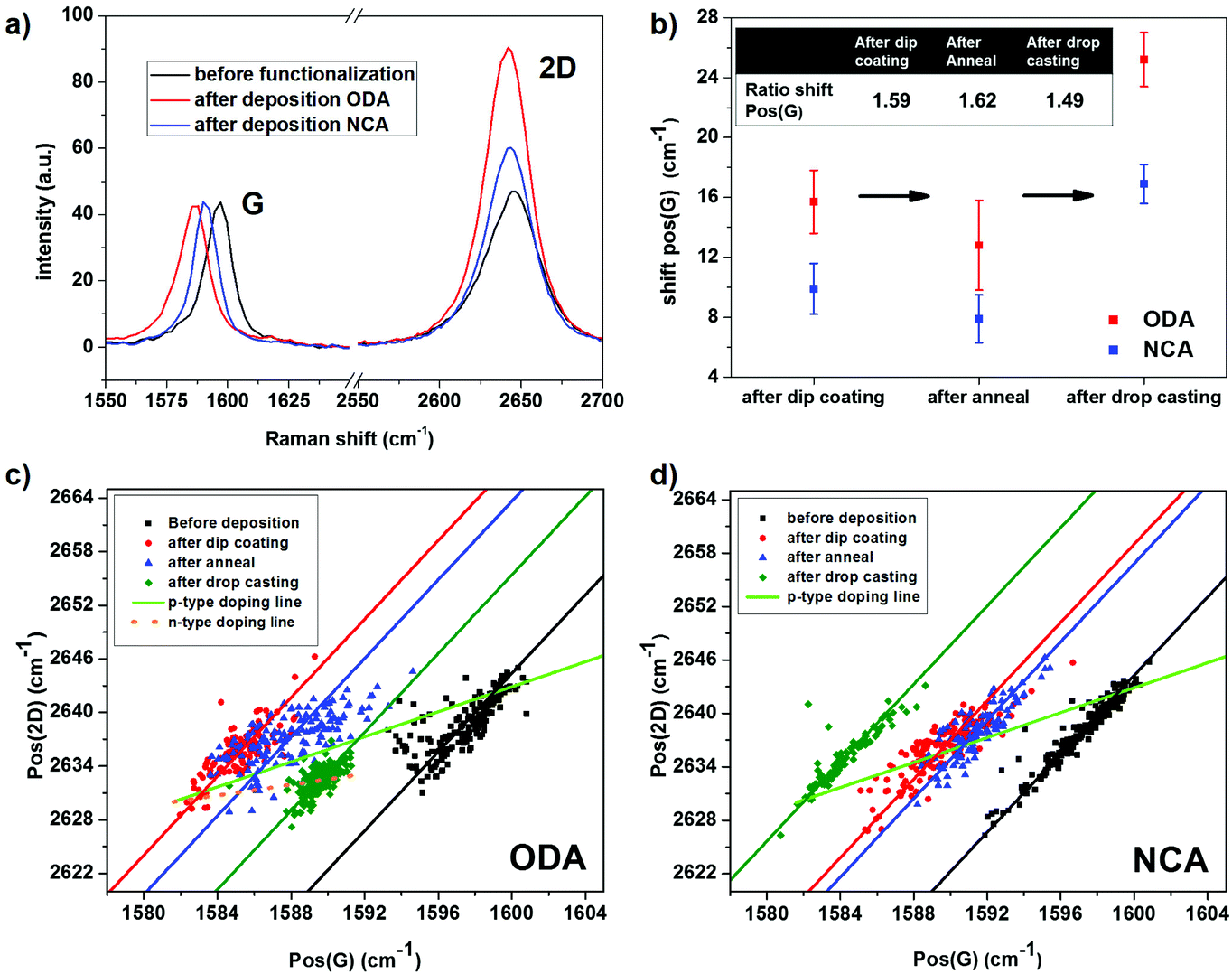 | ||
| Fig. 3 Raman characterization of doping CVD grown graphene using ODA and NCA. (a) Typical Raman spectra of CVD grown graphene before and after deposition of ODA and NCA. (b) Average total shifts of Pos(G), after deposition via dip coating, after subsequent annealing and then drop casting a thick film. Plots of Pos(2D) versus PoS(G) for ODA (c) and NCA (d) functionalized samples before and after deposition via dip coating, after subsequent annealing and after deposition of a thick film using drop casting. The lines fitted through the data points with a (ΔPos(2D)/ΔPos(G)) of 2.2 ± 0.2 correspond to the strain lines. The shift of the data points to higher wavenumbers after drop casting ODA (3c) indicates that upon further increase of doping the Fermi level crossed the Dirac point and moved into the conduction band. | ||
For a fully quantitative analysis of the doping effect however, multiple measurements at different positions on each sample need to be conducted. Therefore, a large number of Raman spectra, 3 Raman maps each containing 100 spectra, were collected on each sample before and after functionalization. The data is corrected for defect areas and bilayer spots by removing data points with a high D peak and an abnormal I(2D)/I(G) ratio (see ESI Fig. S4 and S5† for details). Moreover, the effects of strain induced by the corrugation of the SiO2 substrate must also be considered. As both Pos(G) and Pos(2D) are sensitive to strain as well as doping, variations in peak positions caused by spatial variation in strain are removed using a method based on work by Ryu et al.38 In this method, the contributions of doping and strain are separated by correlating the spatial variation in the G-peak position with that of the 2D-peak position. In a plot of Pos(2D) versus Pos(G), points with varying strain but an identical amount of doping fall on a single line with a slope (ΔPos(2D)/ΔPos(G)) of 2.2 ± 0.2, whereas upon p-type doping without any variation in strain, the points shift along a line with a ΔPos(2D)/ΔPos(G) of 0.7 ± 0.05.38,39 Based on these facts, a line can be drawn in this Pos(G)–Pos(2D) space that represents modulation in hole-doping of strain-free graphene. The point on this line corresponding to charge neutrality can be estimated by the G and 2D peak positions of suspended graphene (1581.6, 2630 cm−1), which is essentially strain-free and undoped.40 Accordingly, for every point in the Pos(G)–Pos(2D) space corresponding to a certain amount of p-type doping and strain, the peak positions that relate to the same amount of doping in the absence of strain is given by projecting this point onto the line representing p-type doping of strain-free graphene.
Fig. 3c and d map the 2D peak positions versus the G peak positions for NCA and ODA before deposition, after deposition via dip coating and after subsequent annealing. Both before and after deposition, the data points are distributed along a line with a slope of ≈2.2 (see lines fitted through data points) indicating that there is a large variation in strain across the samples. By using the aforementioned method, the average peak positions corresponding to the amount of doping without strain-effects can be estimated, with the average values detailed in Table 1. After deposition of the compounds, the mean G peak position, corrected for strain effects, red shifts 15.7 ± 2.1 cm−1 for ODA and 9.9 ± 1.7 cm−1 for NCA (Fig. 3b). Since the G-peak position is approximately linearly dependent on the charge carrier concentration in this spectral range, the ratio of the doping effect can be readily determined from the ratio of the shifts observed in the G peak positions. This ratio is 1.59 based on the observed G peak shifts, and thus is in excellent agreement with what is expected on the basis of the difference in the amine group density on the surface determined using STM. The comparative Raman analysis of ODA and NCA functionalization presented above thus clearly demonstrates that the extent of doping is controlled by the length of the alkyl spacer in the self-assembled network. Although, the functionalized graphene samples showed improvement in film quality after annealing, Raman experiments revealed a concomitant decrease in the n-type doping effect for both compounds. This reduction may be caused by a decrease in the molecular film thickness, as it has been reported that long chain alkyl amines can be vaporized at temperatures as low as 100 °C.41 The ratio between the extents of doping however remained around 1.6.
| Pos(G) (cm−1) | Pos(2D) (cm−1) | FWHM(G) (cm−1) | I(2D)/I(G) | I(D)/I(G) | ||
|---|---|---|---|---|---|---|
| ODA | Before deposition | 1599.0 ± 1.6 | 2642.1 ± 1.1 | 11.3 ± 1.6 | 0.8 ± 0.1 | 0.07 ± 0.11 |
| After dip coating | 1583.2 ± 1.4 | 2631.1 ± 1.4 | 15.4 ± 1.8 | 1.7 ± 0.2 | 0.14 ± 0.19 | |
| After anneal | 1586.1 ± 2.5 | 2633.2 ± 1.7 | 12.7 ± 2.3 | 1.3 ± 0.3 | 0.14 ± 0.19 | |
| After drop casting | 1589.5 ± 0.7 | 2632.4 ± 0.2 | 9.6 ± 1.2 | 1.1 ± 0.1 | 0.04 ± 0.07 | |
| NCA | Before deposition | 1599.0 ± 0.8 | 2642.2 ± 0.5 | 11.1 ± 1.6 | 1.0 ± 0.1 | 0.06 ± 0.05 |
| After dip coating | 1589.2 ± 1.5 | 2635.3 ± 1.1 | 11.8 ± 1.2 | 1.5 ± 0.2 | 0.05 ± 0.09 | |
| After anneal | 1591.2 ± 1.4 | 2636.8 ± 1.0 | 11.8 ± 1.3 | 1.4 ± 0.1 | 0.06 ± 0.08 | |
| After drop casting | 1582.1 ± 1.0 | 2630.3 ± 0.7 | 17.0 ± 1.6 | 2.3 ± 0.1 | 0.17 ± 0.09 | |
To exclude the possibility that the difference in doping is caused by a discrepancy in the amount of the material present on the surface, an additional experiment was performed where a large amount of the material, 3 × 10⁻⁹ mol cm−2, was drop cast after annealing. From the experimentally obtained unit cell parameters (STM), the surface density required for a full monolayer coverage of ODA can be calculated to be 1.4 × 10⁻¹⁰ mol cm−2, and therefore the amount of drop cast material should give more than 20 monolayers for both ODA and NCA, assuming that the material is homogeneously distributed on the surface. It has previously been reported that mainly the first few layers of molecular dopants significantly contribute to the charge transfer doping effect,11 and hence 20 monolayers are enough to ensure that the maximum extent of doping is achieved. Upon drop casting NCA, Pos(G) shifts to lower wavenumbers, indicating that the doping amount increased. The final peak position is very close to the position of charge neutral graphene, hence, the initial amount of p-type doping before functionalization is almost completely counterbalanced by NCA. In contrast to NCA, for ODA there is a shift to higher wavenumbers after addition of more material via drop casting. As a reduction in n-type doping is highly improbable after addition of more material, the upshift after addition of ODA stems from the fact that upon further n-type doping the Fermi level crossed the Dirac point and moved into the conduction band. This explanation is further supported by the slight decrease of Pos(2D) after drop casting ODA. The total shifts of the G-peak relative to the position before deposition are now 25.2 ± 1.8 cm−1 for ODA and 16.9 ± 1.3 cm−1 for NCA, which results in a ratio of the doping effect of 1.49. Thus, despite the large increase in doping, the ratio of the extent of charge transfer doping by the two molecules did not change significantly, which further demonstrates that the doping magnitude is controlled by the length of the alkyl chains. In addition, the further increase in doping after addition of a large amount of material suggests that a significant part of the observed doping can be attributed to an alignment of molecular dipoles, as charge transfer due to orbital mixing typically takes place between molecules directly in contact with graphene. Note that for the case where the Fermi level is in the conduction band, the assumption is made that the line corresponding to strain-free n-type doping can be approximated to be linear for small doping levels, with a ΔPos(2D)/ΔPos(G) of 0.3.38,42 Systematic control experiments revealed that neither toluene nor ethanol causes n-type doping of graphene (ESI Fig. S6†).
To confirm that deposition of the molecules does not induce defects in graphene, the intensity ratio of the D and G peaks (I(D)/I(G)) is analyzed. For defect free graphene the D peak is not present, however, it appears in the presence of crystallographic defects, like sp3-hybridized carbon, and its intensity grows with an increasing defect density. After deposition of ODA via dip coating, I(D)/I(G) increases and remains the same after subsequent annealing, see Table 1. However, drop casting additional material results in a decrease of this intensity ratio. These observations can be explained by the fact that, similar to I(2D)/I(G), I(D)/I(G) is doping dependent.32 The decrease of the intensity ratio after drop casting ODA suggests that the increase after dip coating is not the result of an increase of the defect density, but merely the result of modulation of the intensity by shifts in the Fermi level. This explanation is supported by the behavior of I(D)/I(G) after addition of NCA; there is only an increase after drop casting, where the Fermi level is close to the Dirac point. In line with the physisorbed nature of the doping method, it can be concluded that deposition of the molecules does not result in a significant increase of the defect density.
In parallel to the Raman studies, doping with the self-assembled networks was also assessed through electrical measurements of four-probe, back gated graphene field effect transistors (4P-FET). Two sets of 5 devices were fabricated using CVD grown graphene transferred to 90 nm SiO2 covered highly doped Si substrates. For the device fabrication, graphene was first patterned by photo-lithography and etched with oxygen plasma. The source, drain and voltage probe electrodes were thereafter patterned again using photo-lithography followed by metal contact deposition (Pd 50 nm) and subsequent liftoff. A sketch of the device can be seen in Fig. 4a, as well as an optical micrograph in the inset of Fig. 4b.
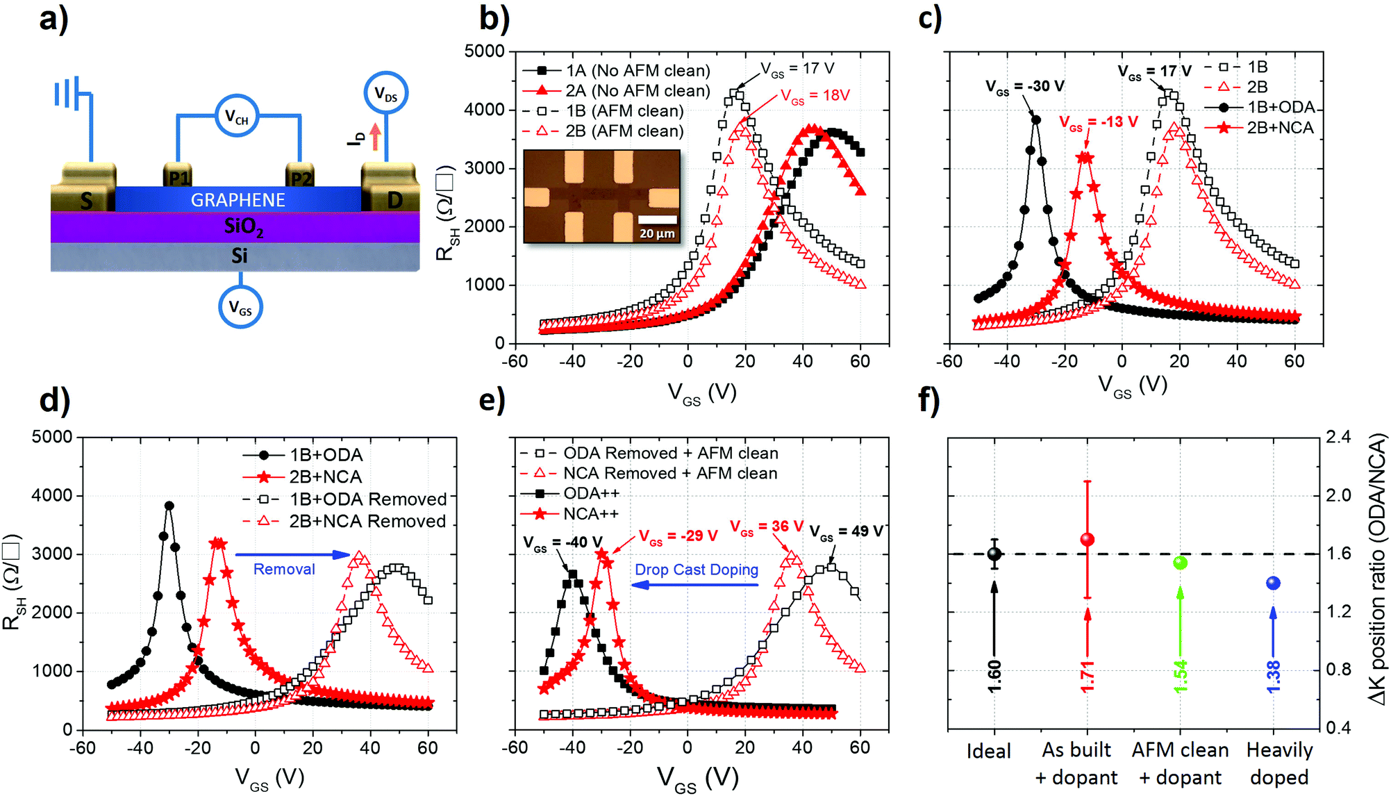 | ||
| Fig. 4 Characterization of doping of graphene using ODA and NCA via electrical characterization of FET devices (devices 1 and 2). (a) Schematic of four-probe back gated graphene FET used for electrical characterization. (b) Transfer characteristics of devices before and after mechanical cleaning using AFM. (c) Transfer characteristics of devices before and after functionalization with ODA and NCA via dip coating. (d) Transfer characteristics of devices doped and after dopant removal. (e) Transfer characteristics after doping by drop casting. (f) Ratio between the doping effect induced on the devices by ODA and NCA. | ||
After fabrication, AFM was used to assess the amount of contamination on the devices, where the root mean square (RMS) surface roughness was taken as a measure of the degree of contamination. The high surface roughness of the graphene channel after fabrication in comparison to the pristine graphene (0.82 nm versus 0.20 nm) indicates that residues were introduced during the development of the devices (ESI Fig. S7†). In order to reduce this contamination, one device of each set was cleaned by mechanical scratching using AFM. In this method, the residues are removed by sweeping them away with the AFM tip, whilst the machine is operated in contact mode.43 After mechanical cleaning, the RMS roughness was reduced to 0.19 nm, indicating that most of the contamination was removed (ESI Fig. S7†).
For electrical characterization, a fixed potential difference was applied between the source and drain electrodes (VDS), inducing a current to circulate from the source to the drain (ID). ID is then modulated by the potential applied to the highly doped Si back gate (VGS) while measuring the potential drop in the channel through the potential probes P1 and P2 (VCH). This method allows extraction of the exact potential drop in the channel without it being affected by the metal/contact interface parasitic resistance. The sheet resistance of the device is then extracted as RSH = (WCH/LCH) (VCH/ID), where WCH is the channel width (5 μm, 20 μm or 50 μm) and LCH is the distance between P1 and P2 (25 μm).
Of the two device sets, the first (1) was used to characterize doping by ODA and the second (2) to characterize doping by NCA. In Fig. 4b, RSH as a function of VGS (transfer curve) of two devices from each set is plotted, before (A) and after (B) AFM cleaning. The highest peak of RSH (K point) corresponds to the point where the Fermi level crosses from the conduction band (electron transport) to the valence band (hole transport) or vice versa. Ideally, for a neutral device with an equal amount of electrons and holes, this RSH peak occurs for VGS = 0. If the K point is shifted towards a more positive VGS in the transfer curve, graphene is p-type doped as more electrons need to be injected by the gate to reach the K point. Conversely, a shift towards a more negative VGS signifies n-type doping. From the position of the K point (VK) in the transfer curve, the ungated carrier concentration (n2D) can be estimated as n2D = (VKCOX)/qe, where COX is the oxide capacitance (3.80 × 10⁻⁸ F cm−2) and qe is the electron charge (1.60 × 10⁻¹⁹ C).1 The carrier mobility is calculated from the sheet conductance (GSH = 1/RSH) as μ4P-FET = (dGSH/dVGS)(1/COX). The extracted parameters from all the devices can be seen in the ESI (Table S1†). In Fig. 4b, a clear shift of VK from 50 V and 43 V in the as-built devices to 17 V and 18 V in the AFM cleaned devices can be seen. The high VK from the as-built devices indicates that they are heavily p-type doped after fabrication and the shift to lower values after cleaning indicates that a considerable part of this p-type doping can be attributed to residues from device processing.
After these initial measurements, the two sets were functionalized by dip coating following the same procedure as described previously. The RSH plotted versus VGS for the cleaned devices before and after functionalization can be seen in Fig. 4c. In device 1B (AFM cleaned) a clear shift can be seen from 17 V to −30 V after functionalization with ODA and from 18 V to −13 V in device 2B (also AFM cleaned) after functionalization with NCA. This shift corresponds to an injection of 11.2 × 1012 cm−2 electrons in device 1B from the ODA self-assembled networks and of 7.4 × 1012 cm−2 for device 2B from NCA. As expected, the amount of electrons injected in the device functionalized with NCA is smaller than that for the ODA device. Interestingly, the ratio of the ODA injected electrons to that of the NCA injected is 1.52, which is in good agreement with the density ratio of amine groups observed previously with STM (1.6 ± 0.1) and with the ratio obtained from the Raman analysis (1.59). This agreement between different types of experiments supports the hypothesis that the doping magnitude is controlled by the length of alkylamine molecules and thus in turn by the density of dopant functional groups in contact with the graphene surface.
For device 1 and 2 the electron (hole) mobility after cleaning with the AFM was 333 (1325) and 496 (1525) cm2 V−1 s−1, respectively. After doping via dip coating the electron (hole) mobility was 1530 (1455) and 1106 (2322) cm2 V−1 s−1 for the same devices. This increase in mobility after doping is explained by the screening of charge impurities by the increase of carriers, thereby reducing coulomb scattering, and further demonstrates the non-destructive nature of the doping method. Furthermore, AFM measurements carried out directly on the devices revealed that the self-assembled networks formed on the devices are similar to those observed on HOPG and CVD graphene (ESI Fig. S9†).
The self-assembled networks were then removed by immersion of both samples in toluene for 8 h at room temperature followed by acetone for 5 min at 50 °C. Thereafter, the samples were dipped in isopropanol and annealed for 8 h at 200 °C with a continuous flow of Ar for 90 min at a chamber pressure of 3 × 10⁻³ mbar and finally cleaned with AFM. It can be seen from Fig. 4 that the doping effect is reversed completely. We note that the devices do not revert to the same doping levels as those measured after cleaning. The higher extent of p-type doping in comparison with the devices after cleaning can be explained by the re-deposition of processing residues from the sample on the devices during immersion in the solvents or an increased interaction with a substrate due to the thermal annealing step.
Subsequently, the samples were functionalized again using dip coating and annealed on a hot plate for 1 min at 100 °C. In accordance with the Raman measurements, there is a reduction in the doping magnitude after annealing the devices functionalized with ODA and NCA, see ESI Fig. S8.† Next, the devices were doped by drop casting to increase the thickness of the molecular dopant films, the results of which are represented in Fig. 4e. After drop casting, there is a larger shift in VK compared to the functionalization using dip coating (−40 V and −29 V for ODA and NCA). Similarly, as in the Raman experiments, this lower VK corresponds to a higher amount of doping compared to that after dip coating. However, the doping ratio between the two compounds after this deposition stage was found to be 1.38 (Fig. 4f), which further suggests that even for thicker films the amount of doping is mainly controlled by the density of the amine groups within the self-assembled networks.
Additionally, the effect of alkylamine functionalization on the as-built devices (without AFM cleaning) was also studied. The n2D of the as built devices was extracted and the results are shown in Fig. 5. Clearly, the amount of electrons injected increases as the length of the molecule decreases. Furthermore, the ratio of the injected n2D for the NCA and ODA functionalized devices yielded an average value of 1.71, close to the expected 1.6 for an ideal device (Fig. 4f) further indicating that the functionalization process is uniform across all different samples. The higher value of the ratio can be linked to the presence of residues before and after functionalization.
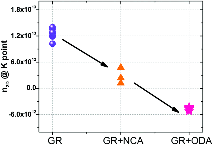 | ||
| Fig. 5 Transport characterization of devices without AFM cleaning. The figure shows the 2D carrier concentration at the K points for devices before and after functionalization with ODA and NCA. | ||
Conclusions
A bottom-up strategy for tuning the Fermi level of graphene is presented based on controlling the density of doping moieties in self-assembled networks via rational design of molecular building blocks. Using a combination of scanning probe microscopy, Raman spectroscopy and electrical measurements on graphene field-effect devices, precise molecular ordering was determined and related to the amount of doping. The relative amount of doping was in excellent agreement with the difference in dopant density on the graphene surface.This non-destructive strategy for precisely controlling the properties of graphene holds promise not only for doping graphene, but also for opening a tunable bandgap in bilayer graphene or functionalization of other 2D materials. In addition, using the rich world of supramolecular chemistry on surfaces, more intricate nanostructures can be envisioned. For example, bicomponent systems consisting of p-type and n-type building blocks offer the possibility to create ordered, spatially varying potentials in graphene. Furthermore, nanoporous networks can be used for the selective adsorption of guest molecules on graphene for sensing. Considering the technological relevance of graphene and other 2D materials, this research direction will pave the path for the transition of self-assembled networks from the field of science towards its application in technology.
Acknowledgements
The authors thank the laboratory personnel, N. Pinna, K. Baumans, J. De Cooman, R. Verheyen, E. Vandenplas and M. Lux for their excellent technical work. This research is supported by the Beyond CMOS program at imec, the Research Foundation-Flanders, Belgium (FWO), internal funds – KU Leuven, and the European Research Council under the European Union's Seventh Framework Programme (FP7/2007–2013) ERC Grant Agreement no. 340324.Notes and references
- K. S. Novoselov, A. K. Geim, S. V. Morozov, D. Jiang, Y. Zhang, S. V. Dubonos, I. V. Grigorieva and A. A. Firsov, Science, 2004, 306, 666–669 CrossRef CAS PubMed.
- A. C. Ferrari, F. Bonaccorso, V. Fal'ko, K. S. Novoselov, S. Roche, P. Boggild, S. Borini, F. H. L. Koppens, V. Palermo, N. Pugno, J. A. Garrido, R. Sordan, A. Bianco, L. Ballerini, M. Prato, E. Lidorikis, J. Kivioja, C. Marinelli, T. Ryhanen, A. Morpurgo, J. N. Coleman, V. Nicolosi, L. Colombo, A. Fert, M. Garcia-Hernandez, A. Bachtold, G. F. Schneider, F. Guinea, C. Dekker, M. Barbone, Z. Sun, C. Galiotis, A. N. Grigorenko, G. Konstantatos, A. Kis, M. Katsnelson, L. Vandersypen, A. Loiseau, V. Morandi, D. Neumaier, E. Treossi, V. Pellegrini, M. Polini, A. Tredicucci, G. M. Williams, B. Hee Hong, J.-H. Ahn, J. Min Kim, H. Zirath, B. J. van Wees, H. van der Zant, L. Occhipinti, A. Di Matteo, I. A. Kinloch, T. Seyller, E. Quesnel, X. Feng, K. Teo, N. Rupesinghe, P. Hakonen, S. R. T. Neil, Q. Tannock, T. Lofwander and J. Kinaret, Nanoscale, 2015, 7, 4598–4810 RSC.
- F. Schwierz, Nat. Nanotechnol., 2010, 5, 487–496 CrossRef CAS PubMed.
- K. Rana, J. Singh and J.-H. Ahn, J. Mater. Chem. C, 2014, 2, 2646–2656 RSC.
- Y. Shi, K. K. Kim, A. Reina, M. Hofmann, L.-J. Li and J. Kong, ACS Nano, 2010, 4, 2689–2694 CrossRef CAS PubMed.
- Y. Kim, J. Ryu, M. Park, E. S. Kim, J. M. Yoo, J. Park, J. H. Kang and B. H. Hong, ACS Nano, 2014, 8, 868–874 CrossRef CAS PubMed.
- H. Wang, T. Maiyalagan and X. Wang, ACS Catal., 2012, 2, 781–794 CrossRef CAS.
- B. Cai, S. Zhang, Z. Yan and H. Zeng, ChemNanoMat, 2015, 1, 542–557 CrossRef CAS.
- F. Schedin, A. K. Geim, S. V. Morozov, E. W. Hill, P. Blake, M. I. Katsnelson and K. S. Novoselov, Nat. Mater., 2007, 6, 652–655 CrossRef CAS PubMed.
- T. Ohta, A. Bostwick, T. Seyller, K. Horn and E. Rotenberg, Science, 2006, 313, 951–954 CrossRef CAS PubMed.
- C. Coletti, C. Riedl, D. S. Lee, B. Krauss, L. Patthey, K. von Klitzing, J. H. Smet and U. Starke, Phys. Rev. B: Condens. Matter, 2010, 81, 235401 CrossRef.
- X. Dong, D. Fu, W. Fang, Y. Shi, P. Chen and L.-J. Li, Small, 2009, 5, 1422–1426 CrossRef CAS PubMed.
- P. Wei, N. Liu, H. R. Lee, E. Adijanto, L. Ci, B. D. Naab, J. Q. Zhong, J. Park, W. Chen, Y. Cui and Z. Bao, Nano Lett., 2013, 13, 1890–1897 CrossRef CAS PubMed.
- K. S. Mali, J. Greenwood, J. Adisoejoso, R. Phillipson and S. De Feyter, Nanoscale, 2015, 7, 1566–1585 RSC.
- A. Ciesielski and P. Samorì, Adv. Mater., 2016, 28, 6030–6051 CrossRef CAS PubMed.
- J. M. MacLeod and F. Rosei, Small, 2014, 10, 1038–1049 CrossRef CAS PubMed.
- Q. Zhou, Y. Li, Q. Li, Y. Wang, Y. Yang, Y. Fang and C. Wang, Nanoscale, 2014, 6, 8387–8391 RSC.
- S. A. Svatek, O. R. Scott, J. P. H. Rivett, K. Wright, M. Baldoni, E. Bichoutskaia, T. Taniguchi, K. Watanabe, A. J. Marsden, N. R. Wilson and P. H. Beton, Nano Lett., 2015, 15, 159–164 CrossRef CAS PubMed.
- Q. H. Wang and M. C. Hersam, Nat. Chem., 2009, 1, 206–211 CrossRef CAS PubMed.
- X. Sun, Y. Mu, J. Zhang, X. Wang, P. Hu, X. Wan, Z. Guo and S. Lei, Chem. – Asian J., 2014, 9, 1888–1894 CrossRef CAS PubMed.
- J. M. MacLeod, J. A. Lipton-Duffin, D. Cui, S. De Feyter and F. Rosei, Langmuir, 2015, 31, 7016–7024 CrossRef CAS PubMed.
- H. Huang, S. Chen, X. Gao, W. Chen and A. T. S. Wee, ACS Nano, 2009, 3, 3431–3436 CrossRef CAS PubMed.
- K. S. Mali, J. Adisoejoso, E. Ghijsens, I. De Cat and S. De Feyter, Acc. Chem. Res., 2012, 45, 1309–1320 CrossRef CAS PubMed.
- R. Gutzler, L. Cardenas and F. Rosei, Chem. Sci., 2011, 2, 2290–2300 RSC.
- M. C. Prado, R. Nascimento, L. G. Moura, M. J. S. Matos, M. S. C. Mazzoni, L. G. Cancado, H. Chacham and B. R. A. Neves, ACS Nano, 2011, 5, 394–398 CrossRef CAS PubMed.
- B. Li, A. V. Klekachev, M. Cantoro, C. Huyghebaert, A. Stesmans, I. Asselberghs, S. De Gendt and S. De Feyter, Nanoscale, 2013, 5, 9640–9644 RSC.
- D. M. Cyr, B. Venkataraman and G. W. Flynn, Chem. Mater., 1996, 8, 1600–1615 CrossRef CAS.
- M. Ishigami, J. H. Chen, W. G. Cullen, M. S. Fuhrer and E. D. Williams, Nano Lett., 2007, 7, 1643–1648 CrossRef CAS PubMed.
- X. Zhang, E. H. Huisman, M. Gurram, W. R. Browne, B. J. van Wees and B. L. Feringa, Small, 2014, 10, 1735–1740 CrossRef CAS PubMed.
- B. Li, K. Tahara, J. Adisoejoso, W. Vanderlinden, K. S. Mali, S. De Gendt, Y. Tobe and S. De Feyter, ACS Nano, 2013, 7, 10764–10772 CrossRef CAS PubMed.
- P. Järvinen, S. K. Hämäläinen, K. Banerjee, P. Häkkinen, M. Ijäs, A. Harju and P. Liljeroth, Nano Lett., 2013, 13, 3199–3204 CrossRef PubMed.
- M. Bruna, A. K. Ott, M. Ijäs, D. Yoon, U. Sassi and A. C. Ferrari, ACS Nano, 2014, 8, 7432–7441 CrossRef CAS PubMed.
- A. Das, S. Pisana, B. Chakraborty, S. Piscanec, S. K. Saha, U. V. Waghmare, K. S. Novoselov, H. R. Krishnamurthy, A. K. Geim, A. C. Ferrari and A. K. Sood, Nat. Nanotechnol., 2008, 3, 210–215 CrossRef CAS PubMed.
- S. Ryu, L. Liu, S. Berciaud, Y.-J. Yu, H. Liu, P. Kim, G. W. Flynn and L. E. Brus, Nano Lett., 2010, 10, 4944–4951 CrossRef CAS PubMed.
- O. Leenaerts, B. Partoens and F. M. Peeters, Phys. Rev. B: Condens. Matter, 2008, 77, 125416 CrossRef.
- J. Moser, A. Verdaguer, D. Jiménez, A. Barreiro and A. Bachtold, Appl. Phys. Lett., 2008, 92, 123507 CrossRef.
- C. Christodoulou, A. Giannakopoulos, M. V. Nardi, G. Ligorio, M. Oehzelt, L. Chen, L. Pasquali, M. Timpel, A. Giglia, S. Nannarone, P. Norman, M. Linares, K. Parvez, K. Müllen, D. Beljonne and N. Koch, J. Phys. Chem. C, 2014, 118, 4784–4790 CAS.
- J. E. Lee, G. Ahn, J. Shim, Y. S. Lee and S. Ryu, Nat. Commun., 2012, 3, 1024 CrossRef PubMed.
- D. Metten, F. Federspiel, M. Romeo and S. Berciaud, Phys. Status Solidi B, 2013, 250, 2681–2686 CrossRef CAS.
- S. Berciaud, X. Li, H. Htoon, L. E. Brus, S. K. Doorn and T. F. Heinz, Nano Lett., 2013, 13, 3517–3523 CrossRef CAS PubMed.
- E. V. Dubrovin, J. W. Gerritsen, J. Zivkovic, I. V. Yaminsky and S. Speller, Colloids Surf., B, 2010, 76, 63–69 CrossRef CAS PubMed.
- A. Das, B. Chakraborty, S. Piscanec, S. Pisana, A. K. Sood and A. C. Ferrari, Phys. Rev. B: Condens. Matter, 2009, 79, 155417 CrossRef.
- A. M. Goossens, V. E. Calado, A. Barreiro, K. Watanabe, T. Taniguchi and L. M. K. Vandersypen, Appl. Phys. Lett., 2012, 100, 073110 CrossRef.
Footnote |
| † Electronic supplementary information (ESI) available: Synthesis of NCA; AFM images of ODA and NCA films on HOPG before and after annealing; AFM images before and after cleaning graphene with toluene; methodology for correcting Raman data; Raman data before and after immersion in ethanol and ethanol/toluene; AFM images of device channels before and after mechanical cleaning with AFM; AFM images of device channel after functionalization with ODA and NCA; transfer curves of GFET devices functionalized with ODA and NCA before and after annealing; a table containing electrical parameters of the devices. See DOI: 10.1039/c6nr07912a |
| This journal is © The Royal Society of Chemistry 2016 |