
 Open Access Article
 This Open Access Article is licensed under a
 Creative Commons Attribution 3.0 Unported Licence
Graphene/nitrogen-functionalized graphene quantum dot hybrid broadband photodetectors with a buffer layer of boron nitride nanosheets†
Hiroyuki
Tetsuka
*,
Akihiro
Nagoya
and
Shin-ichi
Tamura
Frontier Research-Domain, Toyota Central R&D Labs, Inc., 41-1 Yokomichi, Nagakute, Aichi 480-1192, Japan. E-mail: h-tetsuka@mosk.tytlabs.co.jp
First published on 3rd November 2016
Abstract
A high performance hybrid broadband photodetector with graphene/nitrogen-functionalized graphene quantum dots (NGQDs@GFET) is developed using boron nitride nanosheets (BN-NSs) as a buffer layer to facilitate the separation and transport of photoexcited carriers from the NGQD absorber. The NGQDs@GFET photodetector with the buffer layer of BN-NSs exhibits enhanced photoresponsivity and detectivity in the deep ultraviolet region of ca. 2.3 × 10⁶ A W−1 and ca. 5.5 × 10¹³ Jones without the application of a backgate voltage. The high level of photoresponsivity persists into the near-infrared region (ca. 3.4 × 10² A W−1 and 8.0 × 10⁹ Jones). In addition, application in flexible photodetectors is demonstrated by the construction of a structure on a polyethylene terephthalate (PET) substrate. We further show the feasibility of using our flexible photodetectors towards the practical application of infrared photoreflectors. Together with the potential application of flexible photodetectors and infrared photoreflectors, the proposed hybrid photodetectors have potential for use in future graphene-based optoelectronic devices.
Introduction
Graphene has drawn considerable attention due to its outstanding electrical and optical properties. In particular, the broadband absorption of graphene covers the entire ultraviolet range to the far-infrared and its high carrier mobility that reaches 60![[thin space (1/6-em)]](https://www.rsc.org/images/entities/char_2009.gif) 000 cm2 V−1 s−1 makes it a promising candidate material for broadband photodetectors.1 However, the photoresponsivity of graphene photodetectors has been confined to a few milliamps per watt because of the gapless nature of graphene and low light absorption (πα = 2.3%), which prevents efficient photocarrier separation or accumulation.2–4
000 cm2 V−1 s−1 makes it a promising candidate material for broadband photodetectors.1 However, the photoresponsivity of graphene photodetectors has been confined to a few milliamps per watt because of the gapless nature of graphene and low light absorption (πα = 2.3%), which prevents efficient photocarrier separation or accumulation.2–4
There have been several approaches to enhance the performance of graphene by either the integration of graphene with plasmonic nanostructures5–7 or microcavities,8,9 or by utilizing heterostructures of double-layer graphene10 and crumpled graphene,11 which can enhance the light–graphene interaction and improve the photoresponsivity. However, the photoresponsivity is limited to less than 0.1 A W−1, and the complicated fabrication processes and high manufacturing costs make it difficult for graphene to be put to practical use. An excellent alternative approach is to combine graphene with a highly photon-absorbing material. High photoresponsivity and photoconductive gain of up to ca. 107 A W−1 and ca. 108 electrons per photon have been reported for hybrid sensitized graphene photodetectors using colloidal PbS or ZnO quantum dots (QDs) as light-absorbing media.12–15 On the other hand, graphene quantum dots (GQDs), nanometer-sized fragments of graphene, are of great interest as light-absorbing media because their strong confinement and edge effects produce exceptional optical absorption and fluorescence properties. The combination of two-dimensional (2D) materials and GQDs has a unique band alignment which favors selective transfer of photogenerated carriers from GQDs to 2D materials. A photoresponsivity exceeding 107 A W−1 at the ultraviolet (UV) wavelength was observed in graphene/GQD hybrid photodetectors.16,17 The photodetectors based on the hybrid of MoS2 and GQDs have also been reported to provide a high photoresponsivity of 104 A W−1 at the visible wavelength.18 Recently, the broadband photodetection range from UV to near infrared wavelengths was demonstrated for photodetectors consisting of multi-layer GQDs sandwiched between graphene sheets, but their photoresponsivity was limited to 0.2–0.5 A W−1.19 We also recently produced an ultrahigh photoconductivity gain photodetector that utilizes a hybrid consisting of graphene and nitrogen-functionalized graphene quantum dots (NGQDs).20 The high gain in photoconductivity was a consequence of strong light absorption and long-lived photogenerated carriers in the NGQDs. In addition to strong light absorption, NGQDs have bandgap tunability that covers a range of absorption from deep-ultraviolet to infrared,21,22 and can thus be extended to exploit broadband photodetection with high photoresponsivity for graphene-based hybrid photodetectors.
One solution that can be used to boost the performance of graphene-based hybrid photodetectors is to control the band discontinuity of the graphene and the photo-absorbing media by insertion of a buffer layer. Here, we report on the performance of a graphene/NGQD hybrid broadband photodetector with boron nitride nanosheets (BN-NSs) as a buffer layer. Diaminonaphthalene-functionalized graphene quantum dots (DAN-GQDs) with a small bandgap of ca. 1.3 eV were employed for the NGQD layer to enable broadband light detection. Insertion of the BN-NS layer is intended to prevent the recombination of photoexcited carriers at the interface with the graphene/NGQD layer and facilitate the transport of photogenerated electrons from the NGQD layer to graphene, through the vacancy states of BN-NSs formed in the bandgap near the lowest unoccupied molecular orbital (LUMO) levels of the DAN-GQDs. A much faster response time and high photoresponsivity are expected as a result. Application of the graphene/DAN-GQDs with BN-NSs as a buffer layer (DAN-GQDs/BN-NSs@GFET) is demonstrated in a flexible photodetector by the fabrication of the structure on a polyethylene terephthalate (PET) substrate. The feasibility of using our flexible photodetectors towards the practical application of infrared photoreflectors is also shown.
Experimental
Materials
Graphite nanoparticles (GNPs; <50 nm, SkySpring Nanomaterials, Inc.) were used as a precursor for the preparation of the DAN-GQDs. BN-NSs (ethanol/water dispersion) were obtained from Graphene Laboratories, Inc. 2,3-Diaminonaphthalene (DAN) was obtained from Tokyo Chemical Industry Co., Ltd. N,N-Dimethylformamide (DMF) as a solvent, and sulfuric acid and nitric acid as oxidizing agents were obtained from Wako Pure Chemical Industries.Synthesis of DAN-GQDs
DAN-GQDs were prepared by a hydrothermal reaction using DAN, as shown in Fig. 1a. During the reaction process, phenazine and benzoimidazole skeletons were introduced into the graphene lattice by nucleophilic substitution of the double –NH2 in DAN with the hydroxyl groups of oxidized GQDs (o-GQDs). A typical procedure for the preparation of DAN-GQDs is given as follows. 5 mL of o-GQDs were dispersed in water (ca. 1 mg mL−1) and mixed with 2.5 mg of DAN. The o-GQDs were obtained by refluxing GQDs delaminated from GNPs in a 2:1 solution of concentrated H2SO4 and HNO3. The mixture was ultrasonicated for 30 min and then transferred to a poly(tetrafluoroethylene) (Teflon)-lined autoclave (45 mL capacity) where it was heated to 180 °C for 12 h. After cooling to room temperature, the suspension was dialyzed and centrifuged at 13400 rpm for 30 min. The precipitates were re-dispersed in DMF and centrifuged at 13400 rpm for 30 min to filter out large, insoluble fragments.
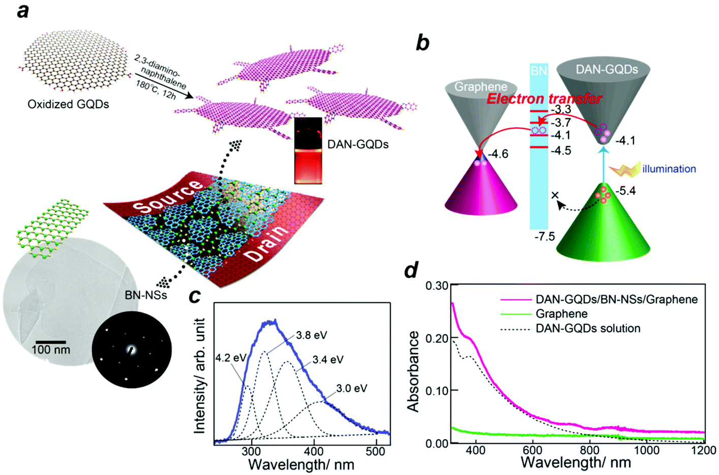 | ||
| Fig. 1 (a) Schematic representation of a DAN-GQD/BN-NS@GFET hybrid photodetector. (b) Schematic of the energy level alignment for the photodoping effect under illumination. Only the photoexcited electrons in the DAN-GQDs were transferred to the graphene layer through the vacancy states formed in the bandgap of BN-NSs, and the recombination of the photoexcited carriers at the interface of graphene/DAN-GQDs was suppressed. (c) Cathodeluminescence spectrum of the BN-NSs. A broad emission peak is distributed from 260 nm to 500 nm, which respectively locates at 292 nm (4.2 eV), 320 nm (3.8 eV), 356 nm (3.4 eV) and 410 nm (3.0 eV). This characteristic peak may originate from B vacancies and residual C or O impurities. (d) UV-vis-NIR absorption spectra of graphene and the DAN-GQD/BN-NS/graphene film on PET substrates. The broken line represents the DNA-GQD solution. | ||
Photodetector device fabrication
Monolayer graphene sheets formed by chemical vapor deposition (CVD) onto a p-doped Si wafer (525 μm, 0.002 Ω cm, 90 nm SiO2 layer) were obtained from Graphene Platform Corp. The source and drain electrodes were directly formed on the top of the graphene/Si wafer. The patterns of source and drain contacts to graphene were defined using a conventional photolithography process with a poly(methyl methacrylate) resist. The contacts were formed with titanium and gold (15 nm per 100 nm) using a sputtering deposition method, followed by a lift-off process. These devices had an effective channel length L of 10 μm and a channel width W of 10 μm. After the gate contact was deposited onto the back side of the Si wafer, the device was diced into 1 × 1 cm substrates, and the BN-NS and DAN-GQD dispersions were dropped directly onto the top of each substrate, subsequently.Fabrication of the flexible photodetector was achieved by replacement of the Si substrate with a PET substrate. Monolayer graphene sheets formed by CVD onto a PET substrate (188 μm) were obtained from Graphene Platform Corp. The source and grain electrodes were also directly fabricated on the top of the graphene/PET substrate. The contacts were formed with gold (100 nm) using a sputtering deposition method, through a metal shadow mask. These devices had an effective channel length L of 80 μm and a channel width W of 200 μm.
Photoresponse measurements
Photoresponse measurements were performed using a confocal microscope. A light source was guided into the microscope through an optical fiber and focused with a 10× objective lens. Laser diodes or light-emitting diodes (LEDs) with various wavelengths were used as light sources to provide light with wavelengths of 254, 365, 440, 617, 785, and 940 nm. A ϕ 50 μm core optical fiber (the resulting spot size of light is ϕ 5 μm) was used for light sources (440 nm, 617 nm, 785 nm, and 940 nm). A ϕ 200 μm core optical fiber (the resulting spot size of light is ϕ 20 μm) was used for shorter-wavelength light sources (254 nm and 365 nm). The optical power was calibrated by using a silicon photodetector (Thorlabs, S130VC). Electrical measurements were performed using a Keithley 2602A system source meter in conjunction with LabVIEW software. All measurements were conducted at room temperature under the ambient atmosphere.Ab initio calculations
The formation energy for a point defect D in a charge state q is expressed by:23,24 | (1) |
| ε(q/q′) = (ΔED,q(EF = 0) − ΔED,q′(EF = 0))/(q′ − q) | (2) |
The calculations were executed using the plane-wave projector augmented wave (PAW) method25,26 with the application of the Heyd–Scuseria–Ernzerhof (HSE)27,28 hybrid functional on the basis of the Perdew–Burke–Ernzerhof (PBE)29 exchange–correlation functional, as implemented in the VASP code.30,31 A plane-wave cut-off of 400 eV was used. The 12 × 12 × 1 k-point sampling was used for Brillouin-zone integration in the primitive cell. Single layer hexagonal BN was modelled using a 7 × 7 × 1 supercell separated by a 15 Å vacuum. The lattice constants were fixed at the optimized constants for perfect hexagonal BN, while ionic positions were relaxed until the residual forces became smaller than 0.01 eV Å−1.
Instrumentation
The cathodoluminescence (CL) properties of the samples were investigated at room temperature using an in-house-built thermal field emission electron microscope equipped with a spectrometer. Optical absorption spectra were recorded using an UV/VIS/NIR spectrophotometer (UV-3600; Shimadzu Corp.). Transmission electron microscopy (TEM) images were recorded on a Hitachi EX-2000 microscope operated at an accelerating voltage of 200 kV. Work function measurements were performed using a photoelectron yield spectrometer (BIP-KV201, Bunkoukeiki Co., Ltd). The height profile was investigated using atomic force microscopy (AFM; NanoscopeV D3100, Veeco Instruments).Results and discussion
Fig. 1a illustrates the structure of the graphene/BN-NS/DAN-GQD photodetector. The substrate was heavily p-doped Si with a 90 nm SiO2 surface layer. Graphene acts as the carrier transport channel, while the BN-NSs act as a buffer layer, and the DAN-GQDs are used as photon absorbers. The BN-NSs were inserted between the graphene and the DAN-GQD layer by dropping the dispersion of BN-NSs in ethanol/water directly on top of the graphene field-effect transistor. The BN-NSs have areas of a few hundreds of square nanometers and consist of 1–5 layers, which uniformly cover the graphene layer (see the insets of Fig. 1a and S1†). The DAN-GQDs were prepared through a hydrothermal reaction of the oxidized GQDs with 2,3-diaminonaphthalene (Fig. S2†).20 The DAN-GQD layer was formed by dropping a dispersion of DAN-GQDs in DMF directly on the top of the BN-NS layer (Fig. S3†). The NGQD film thickness in the photodetector was optimized at ca. 150 nm. The optical absorption of the photodetector was markedly increased by incorporation of the DAN-GQD layer (Fig. 1d). Note that the DAN-GQD film formed on the BN-NS/graphene/PET substrate showed a shift of the absorption edge to longer wavelengths, compared to that of the as-prepared DAN-GQD solution. This can be attributed to the π–π stacking of the individual DAN-GQDs, leading to a lowering in the bandgap.The band alignment at the graphene/BN-NS/DAN-GQD interface under light irradiation is schematically illustrated in Fig. 1b. The BN-NS layer is inserted to prevent the recombination of photoexcited carriers at the NGQD/BN-NS layer interface and to facilitate the transport of photogenerated electrons from the NGQD layer to graphene. Incident photons excite the ground-state electrons of DAN-GQDs into excited states, and then electron–hole pairs are generated. Only electrons are transported into the graphene layer through the vacancy states formed in the bandgap of the BN-NSs, while the photoexcited holes remain in the NGQD layer. The vacancy states formed in the bandgap of the BN-NSs are located between the graphene and DAN-GQD LUMO levels, which facilitates the transport of photogenerated electrons from the NGQD layer to graphene. A much faster response time and high photoresponsivity are expected as a result. The vacancy levels of BN-NS were estimated by subtracting the exciton energy of the vacancy states measured using CL (Fig. 1c) from the highest occupied molecular orbital (HOMO) level. The HOMO level was measured using ultraviolet photoelectron yield spectroscopy (Fig. S4†). These vacancy states may originate from B or N defects and residual C or O impurities.32 The electronic states of vacancy defects and carbon impurities in BN were theoretically estimated (details in Fig. S5†). Theoretical calculations suggested that the N defect in the BN lattice and the substitution of C at a B-site can induce localized energy levels in the bandgap, near the experimentally observed vacancy levels.
Fig. 2a and b show the transfer characteristics (VSD = –0.5 V) of the DAN-GQD/BN-NS@GFET hybrid photodetector and a pristine graphene field-effect transistor. The Dirac point (charge neutrality point, VD) from the pristine graphene transistor was observed at ca. 23 V. After hybridization of the DAN-GQDs, VD shifted to ca. 1.2 V, which suggests that electrons were transferred from DAN-GQDs to graphene. This is consistent with the higher work function of DAN-GQDs. Upon irradiation of the DAN-GQD/BN-NS@GFET hybrid photodetectors, VD shifts to a lower voltage, which suggests that photoexcited electrons are transferred to the graphene. The laser beam (440 nm, 1.3 nW) was focused on an area (∅ = 5 μm) between the source and drain electrodes, which were separated by a 10 μm gap. An asymmetric behaviour in hole and electron conduction branches may originate from the shift of the Fermi level of graphene by hybridization with DAN-GQDs. The hole-carrier mobility increased from ca. 1061 to 1636 cm2 V−1 s−1 by hybridization of the DAN-GQDs/BN-NSs. The increase in carrier mobility may be due to an increase in the density of states near the Fermi level, which was induced by the widely distributed π orbitals of the DAN-GQDs.
 | ||
| Fig. 2 (a) ISD–V curve (VSD = 0.5 V) for the on (440 nm, 1.3 nW) and off states of a DAN-GQD/BN-NS@GFET photodetector. (b) ISD–V curve (VSD = 0.5 V) for a pristine graphene field-effect transistor. (c) Temporal photocurrent response of the DAN-GQD/BN-NS@GFET photodetector (VSD = 0.1 V, VG = 0 V, 440 nm, 420 nW). The dotted line shows the temporal photocurrent response of the DAN-GQD@GFET photodetector without the BN-NS buffer layer. (d) Photoresponsivity as a function of gate voltage. The insets show the direction of electron transfer from DAN-GQDs to graphene for the hole and electron conduction regimes in graphene under illumination. (e) Comparison of photoresponsivities for the photodetectors with and without the BN-NS layer. | ||
Fig. 2c shows the temporal photocurrent (ΔI = Ilight − Idark) response of the DAN-GQD/BN-NS@GFET hybrid photodetector, where the on/off cycle of the laser (VG = 0 V, VSD = 0.1 V and excitation power of 420 nW) was 1 s. A negative value of ΔI was detected. At VG = 0 V, the major carriers in the graphene layer are holes and the transferred electrons diminish the hole concentration, which leads to decreased conductance and a negative ΔI (Fig. 1b). The back-gate dependence of the photoresponsivity (Fig. 2d) is also consistent with the proposed model. We observed a clear carrier type and concentration dependence of the external photoresponsivity Rext (Rext = ΔI/Plight, where Plight is the incident optical power). In the hole-conduction region (VG < 1.2 V), the photoinduced electron carriers diminish the hole concentration, leading to a decreased conductance and a negative-valued Rext. By contrast, the electron concentration increases by the photoinduced electron carriers, which leads to an increased conductance and a positive-valued Rext in the electron-conduction region (VG > 1.2 V). The current of the photodetector was switched on and off effectively and with good repeatability. The rise time was ca. 45 ms (corresponding to ca. 90% rise). The temporal response was markedly improved by insertion of the BN-NS layer, compared to that of the DAN-GQDs@GFET without the BN-NS layer (ca. 700 ms). The decay time remained unchanged. The insertion of the BN-NS layer also enhanced the Rext by more than twofold and extended the detection limit of light (Fig. 2e).
The decay photoresponse dynamics are presented in Fig. 3a under various irradiation powers. The time response of the photocurrent decay is dominated by two components and can be fitted with a double exponential; ΔIDS = ΔI1[1 − exp(−t/τ1)] + ΔI2[1 − exp(−t/τ2)]. For instance, when the power is 420 nW and VG = 0 V, the time constants τ1 and τ2 are 0.69 and 8.5 s, respectively. The decay time of the photodetector can be regarded as the carrier recombination time (lifetime, τlife). The short relaxation time τ1 corresponds to the lifetime of holes in the DAN-GQDs before they are transferred to graphene, whereas the long relaxation time τ2 represents the charge transfer between DAN-GQDs. The photoconductive gain (G = τlife/τtransit = τlife/L2/μ·VDS, where τtransit represents the carrier transit time, L is the channel length, μ is the carrier mobility, and VDS denotes the applied bias) is calculated based on these measurements. The measured transit time of the carrier is ca. 1.22 ns (because μ = 1636 cm2 V−1 s−1, L = 10 μm and VDS = 0.5 V). The predicted range of values for G is between 5.6 × 10⁸ and 6.9 × 10⁹, using lifetimes of 0.69 s and 8.5 s respectively. The high gain is attributed to the long carrier lifetime in the NGQDs and the high mobility of graphene. Multiple carrier circulation occurs in the graphene channel, whereas holes remain trapped in the DAN-GQD layer.
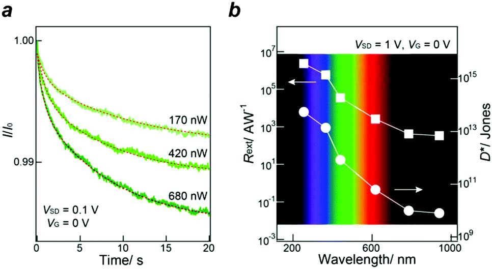 | ||
| Fig. 3 (a) Excitation power dependence of the response time for the DAN-GQD/BN-NS@GFET hybrid photodetector with various irradiation powers from 170 to 680 nW. (b) Photoresponsivity and specific detectivity versus optical irradiation power (laser wavelengths of 254–940 nm) for the DAN-GQD/BN-NS@GFET hybrid photodetector. | ||
Fig. 3b summarizes the wavelength-dependent external photoresponsivity Rext and specific detectivity D* (D* = Rext·APD1/2/(2eIdark)1/2, where APD is the area of the photodetector channel, e is the electron charge, and Idark is the dark current)33 of the DAN-GQD/BN-NS@GFET hybrid photodetector at a fixed bias of 1 V. For calculations at 254 nm and 365 nm, we calculated Rext (Rext = ΔI/(Plight·APD/Alight), where Alight is the light spot area) by inserting the scaling factor (APD/Alight) that takes into account the fact that only a fraction of optical power impinges on the photodetector. The DAN-GQD/BN-NS@GFET hybrid photodetector exhibited high photoresponsivity and detectivity from the deep ultraviolet to the near-infrared region. The Rext and D* were ca. 2.3 × 10⁶ A W−1 and ca. 5.5 × 10¹³ Jones in the deep ultraviolet region, without the application of a backgate voltage. The high level of photoresponsivity and detectivity persisted up to the near-infrared region (ca. 3.4 × 10² A W−1 and ca. 8.0 × 10⁹ Jones at 940 nm). The maximum values of Rext and D* at each wavelength are comparable to those reported for other high performance photodetectors (Table S1†). The increased Rext toward the shorter-wavelength is consistent with the fact that the absorption of the DAN-GQDs is strongly enhanced at high energies. Note that the photocurrent increases linearly with the source–drain bias and high Rext is achieved when the bias voltage is increased and the incident optical power is decreased (Fig. S6†). The decreased Rext with the incident optical power (Fig. S6b†) can be explained considering that the more photogenerated electrons are injected into the graphene channel, the lower the electric field at the DAN-GQD/BN-NS/graphene interface, therefore a reduced injection of electrons causes Rext to decrease.
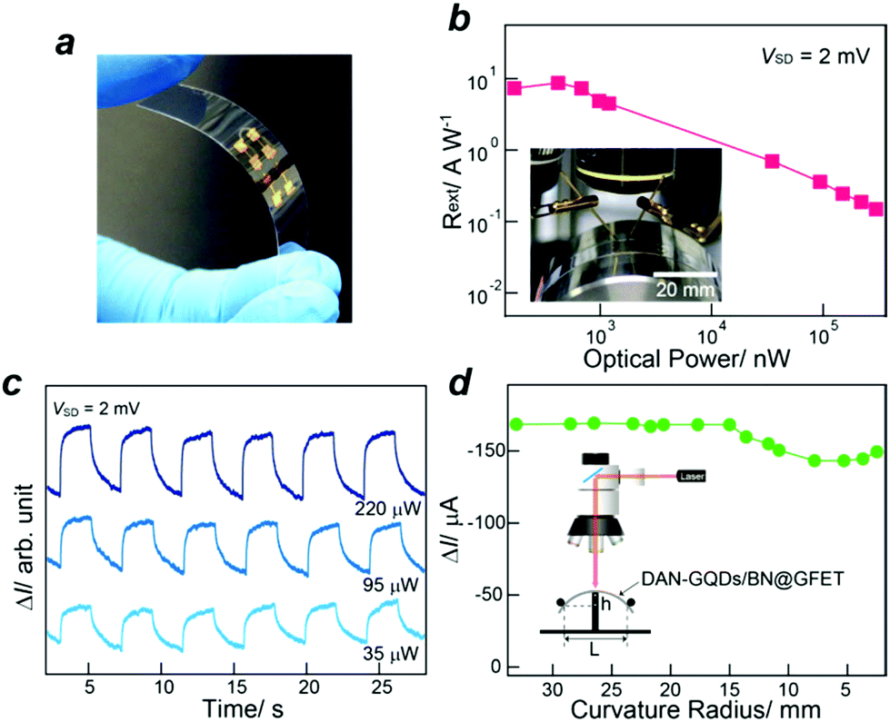
Flexible broadband photodetectors constructed on transparent, lightweight, flexible substrates have attracted wide interest for the development of novel optoelectronic devices. Here, we investigate the application of a flexible photodetector device by constructing the graphene/BN-N/DAN-GQD structure on a PET substrate. Fig. 4a shows a photograph of the flexible DAN-GQD/BN-NS@GFET hybrid photodetector. The flexible photodetector was fabricated by successive drop-casting of BN-NS and DAN-GQD solutions onto patterned Au electrodes (L = 80 μm and W = 200 μm) with CVD-grown graphene transferred to the PET substrate (no backgate electrode). Fig. 4b shows the photoresponsivity of the flexible DAN-GQD/BN-NS@GFET hybrid photodetector with the radius of curvature fixed at 29 mm. Under a low applied bias of 2 mV, the flexible DAN-GQD/BN-NS@GFET hybrid photodetector exhibited a relatively high photoresponsivity of ca. 10 A W−1. The photocurrent is presented as a function of time in Fig. 4c for several cycles under various laser powers. The photoresponse and operation of the flexible DAN-GQD/BN-NS@GFET hybrid photodetector were very stable. We also measured the photocurrent as a function of bending radius rb (rb = [h2 + (L/2)2]/2h, where L is the chord of circumference connecting the two ends of the arc, and h is the height at the chord midpoint) using a three-point bending setup (see the inset of Fig. 4d). Fig. 4d plots the photocurrent as a function of the bending radius. Although a ca. 15% reduction in the photocurrent was observed upon bending at curvatures with <15 mm, the photocurrent was still maintained even at a bending radius of ca. 2 mm without significant degradation.
 | ||
| Fig. 4 (a) Photograph of the flexible and transparent DAN-GQD/BN-NS@GFET hybrid photodetector fabricated on a PET substrate. (b) Photoresponsivity as a function of optical power (light wavelength of 440 nm) for the flexible DAN-GQD/BN-NS@GFET hybrid photodetector. The inset shows a photograph of the photodetector fixed around the cylinder with the curvature radius of 29 mm. (c) On and off photocurrent response dynamics of the flexible DAN-GQD/BN-NS@GFET hybrid photodetector. (d) Photocurrent as a function of the bending radius. The inset shows the schematic illustration of the three-point bending setup. | ||
Finally, we further demonstrate the practical application of an infrared photoreflector for distance measurement and obstacle detection. The infrared photoreflector we designed works by measuring the amount of incident infrared light backscattered from an object. Fig. 5a shows the schematic of the prototype infrared photoreflector mounted on the front panel consisting of “nanoblocks” in conjunction with an open-source electronics platform “arduino uno”, which consists of two infrared LEDs as a light source and a flexible DAN-GQD/BN-NS@GFET hybrid photodetector in the middle. Fig. 5b plots the temporal change in the photocurrent with distance from the object. The clear change of photocurrent with distance was observed, and the photoreflector can measure up to 20 cm in this configuration. Next, we checked the feasibility of using our photoreflector by detecting the presence of an obstacle. The signal from the photoreflector was used to detect the presence or absence of the obstacle. The movie showing the operation of the infrared photoreflector is given in the ESI (Movie S1†). When the photocurrent from the photodetector is increased to the threshold value of the photocurrent being set in the program that controls the detectable distance (in this case, the detectable distance was set to ca. 10 cm), the green-LED is turned on. By contrast, when the photocurrent is decreased to under the threshold value, the green-LED is turned off. The LED of the photoreflector was turned on (Fig. 5c(i)) and off (Fig. 5c(ii)) effectively in the presence or absence of the obstacle. These show that our flexible DAN-GQDs/BN-NSs@GFET has significant potential for use in practical devices.
 | ||
| Fig. 5 (a) Schematic of the prototype infrared photoreflector. The two infrared LEDs radiate the infrared light and when the beam strikes an object it is reflected back towards the DAN-GQD/BN-NS@GFET photodetector. (b) The change in the photocurrent with distance from the object. (c) Digital images (snapshots from Movie S1, ESI†) showing the operation of the infrared photoreflector. The green-LED of the infrared photoreflector was turned on (i) and off (ii) with the presence or absence of the obstacle. | ||
Conclusions
In summary, we have reported a high performance graphene/nitrogen-functionalized graphene quantum dot hybrid broadband photodetector with a buffer layer of boron nitride nanosheets (DAN-GQDs/BN-NSs@GFET). The BN-NS buffer layer facilitated the separation and transport of photoexcited carriers from the DAN-GQD photon absorber to graphene. The DAN-GQD/BN-NS@GFET hybrid photodetector exhibited high photoresponsivity and detectivity over the entire broadband wavelength region. Together with the potential application for flexible photodetectors and infrared photoreflectors demonstrated here, this hybrid photodetector has significant potential for use in future graphene-based optoelectronic devices.Acknowledgements
The authors acknowledge H. Fujikawa and H. Takashima for technical assistance and fruitful discussions.References
- F. Bonaccorso, Z. Sun, T. Hasan and A. C. Ferrari, Nat. Photonics, 2010, 112, 611 CrossRef.
- F. Xia, T. Mueller, Y.-M. Lin, A. Valdes-Garcia and P. Avouris, Nanotechnology, 2009, 4, 839–843 CAS.
- T. Muller, F. Xia and P. Avouris, Nat. Photonics, 2010, 4, 297–301 CrossRef.
- Y. Zhang, T. Liu, B. Meng, X. Li, G. Liang, X. Hu and Q. J. Wang, Nat. Commun., 2013, 4, 1811 CrossRef PubMed.
- T. J. Echtermeyer, L. Britnell, P. K. Jasnos, A. Lombardo, R. V. Gorbachev, A. N. Grigorenko, A. K. Geim, A. C. Ferrari and K. S. Novoselov, Nat. Commun., 2011, 2, 458 CrossRef CAS PubMed.
- Z. Fang, Z. Liu, Y. Wang, P. M. Ajayan, P. Nordlander and N. J. Halas, Nano Lett., 2012, 12, 3808–3813 CrossRef CAS PubMed.
- A. N. Grigorenko, M. Polini and K. S. Novoselov, Nat. Photonics, 2012, 6, 749–758 CrossRef CAS.
- M. Furchi, A. Urich, A. Pospischil, G. Lilley, K. Unterrainer, H. Detz, P. Klang, A. M. Andrews, W. Schrenk, G. Strasser and T. Mueller, Nano Lett., 2012, 12, 2773–2777 CrossRef CAS PubMed.
- M. Engel, M. Steiner, A. Lombardo, A. C. Ferrari, H. V. Löhneysen, P. Avouris and R. Krupke, Nat. Commun., 2012, 3, 906 CrossRef PubMed.
- C.-H. Liu, Y.-C. Chang, T. B. Norris and Z. Zhong, Nat. Nanotechnol., 2014, 9, 273–278 CrossRef CAS PubMed.
- P. Kang, M. C. Wang, P. M. Knapp and S. W. Nam, Adv. Mater., 2016, 28, 4639–4645 CrossRef CAS PubMed.
- G. Konstantatos, M. Badioli, L. Gaudreau, J. Osmond, M. Bernechea, F. P. G. Arquer, F. Gatti and F. H. L. Koppens, Nat. Nanotechnol., 2012, 7, 363–368 CrossRef CAS PubMed.
- Z. Sun, Z. Liu, J. Li, G.-A. Tai, S.-P. Lau and F. Yan, Adv. Mater., 2012, 24, 5878–5883 CrossRef CAS PubMed.
- D. Shao, J. Gao, P. Chow, H. Sun, G. Xin, P. Sharma, J. Lian, N. A. Koratkar and S. Sawyer, Nano Lett., 2015, 15, 3787–3792 CrossRef CAS PubMed.
- W. Guo, S. Xu, Z. Wu, N. Wang, M. M. T. Loy and S. Du, Small, 2013, 9, 3031–3036 CrossRef CAS PubMed.
- S.-H. Cheng, T.-M. Weng, M.-L. Lu, W.-C. Tan, J.-Y. Chen and Y.-F. Chen, Sci. Rep., 2013, 3, 2694 Search PubMed.
- C.-W. Chiang, G. Haider, W.-C. Tan, Y.-R. Liou, Y.-C. Lai, R. Ravindranath, H.-T. Chang and Y.-F. Chen, ACS Appl. Mater. Interfaces, 2016, 8, 466–471 CAS.
- C. Chen, H. Qiao, S. Lin, C. M. Luk, Y. Liu, Z. Xu, J. Song, Y. Xue, D. Li, J. Yuan, W. Yu, C. Pan, S. P. Lau and Q. L. Bao, Sci. Rep., 2015, 5, 11830 CrossRef PubMed.
- C. O. Kim, S. W. Hwang, S. Kim, D. H. Shin, S. S. Kang, J. M. Kim, C. W. Jang, J. H. Kim, K. W. Lee, S.-H. Choi and E. Hwang, Sci. Rep., 2014, 4, 5603 CAS.
- H. Tetsuka, A. Nagoya, T. Fukusumi and T. Matsui, Adv. Mater., 2016, 28, 4632–4638 CrossRef CAS PubMed.
- H. Tetsuka, R. Asahi, A. Nagoya, K. Okamoto, I. Tajima, R. Ohta and A. Okamoto, Adv. Mater., 2012, 24, 5333–5338 CrossRef CAS PubMed.
- H. Tetsuka, A. Nagoya and R. Asahi, J. Mater. Chem. C, 2015, 3, 3536–3541 RSC.
- C. G. Van de Walle and J. Neugebauer, J. Appl. Phys., 2004, 95, 3851–3879 CrossRef CAS.
- S. B. Zhang and J. E. Northrup, Phys. Rev. Lett., 1991, 67, 2339–2342 CrossRef CAS PubMed.
- P. E. Blöchl, Phys. Rev. B: Condens. Matter, 1994, 50, 17953–17979 CrossRef.
- G. Kresse and D. Joubert, Phys. Rev. B: Condens. Matter, 1999, 59, 1758–1775 CrossRef CAS.
- J. Heyd, G. E. Scuseria and M. Ernzerhof, J. Chem. Phys., 2003, 118, 8207–8215 CrossRef CAS.
- J. Heyd, G. E. Scuseria and M. Ernzerhof, J. Chem. Phys., 2006, 124, 219906 CrossRef.
- J. P. Perdew, K. Burke and M. Ernzerhof, Phys. Rev. Lett., 1996, 77, 3865–3868 CrossRef CAS PubMed.
- G. Kresse and J. Furthmüller, Comput. Mater. Sci., 1996, 6, 15–50 CrossRef CAS.
- G. Kresse and J. Furthmüller, Phys. Rev. B: Condens. Matter, 1996, 54, 11169–11186 CrossRef CAS.
- F. Liu, X. Mo, H. Gan, T. Guo, X. Wang, B. Chen, J. Chen, S. Deng, N. Xu, T. Sekiguchi, D. Golberg and Y. Bando, Sci. Rep., 2014, 4, 4211 Search PubMed.
- A. R. Jha, Infrared Technology, Wiley, New York, 2000 Search PubMed.
Footnote |
| † Electronic supplementary information (ESI) available. See DOI: 10.1039/c6nr07707b |
| This journal is © The Royal Society of Chemistry 2016 |