
 Open Access Article
 This Open Access Article is licensed under a Creative Commons Attribution-Non Commercial 3.0 Unported Licence
Robust, directed assembly of fluorescent nanodiamonds†
Mehran
Kianinia
a,
Olga
Shimoni
a,
Avi
Bendavid
b,
Andreas W.
Schell
c,
Steven J.
Randolph
d,
Milos
Toth
*a,
Igor
Aharonovich
*a and
Charlene J.
Lobo
*a
aSchool of Mathematical and Physical Sciences, University of Technology Sydney, P.O. Box 123, Broadway, NSW 2007 Australia. E-mail: Charlene Lobo, charlene.lobo@uts.edu.au; igor.aharonovich@uts.edu.au; m.toth@uts.edu.au
bCSIRO Manufacturing, Lindfield, NSW 2070, Australia
cDepartment of Electronic Science and Engineering, Kyoto University, Kyoto daigaku-katsura, Nishikyo-ku, Kyoto, Japan
dFEI Company, 5350 NE Dawson Creek Dr., Hillsboro, OR 97124, USA
First published on 7th October 2016
Abstract
Arrays of fluorescent nanoparticles are highly sought after for applications in sensing, nanophotonics and quantum communications. Here we present a simple and robust method of assembling fluorescent nanodiamonds into macroscopic arrays. Remarkably, the yield of this directed assembly process is greater than 90% and the assembled patterns withstand ultra-sonication for more than three hours. The assembly process is based on covalent bonding of carboxyl to amine functional carbon seeds and is applicable to any material, and to non-planar surfaces. Our results pave the way to directed assembly of sensors and nanophotonics devices.
Assembling fluorescent nanoparticles into macroscopic arrays is required for many applications spanning sensing,1,2 photonics, plasmonics and quantum information processing.3–5 To achieve this goal several top down techniques, including lithography6,7 or dip-pen techniques,8,9 as well as bottom up methods using patterned self-assembled monolayers,10 electrostatic self-assembly11,12 and DNA origami13,14 have been developed. While these methods are capable of high resolution patterning of nanoparticle arrays, the assembled components are only weakly bonded to the substrate and cannot undergo further wet chemistry processing steps (e.g. sonication) or subsequent lithography. Such processing is often required for device applications where the fluorescent nanoparticles act as active components in microfluidic devices,15,16 as sensing probes17 or photon sources in which they are coupled to plasmonic structures or other optical elements.18–20
In particular, there is a great interest in controlling and positioning fluorescent nanodiamonds that host nitrogen vacancy (NV−) defects, which can then be employed as nanoscale sensors for detection and imaging of weak magnetic fields,1,21,22 thermal imaging or thermometry23–25 and quantum measurements.26–28 Moreover, there is a great interest in assembling arrays of nanodiamonds29,30 that can subsequently be used to couple to plasmonic waveguides to realize quantum plasmonics circuitry.20,31,32 However, unlike gold nanoparticles, which can be assembled into arrays using SAMs and block copolymer templates,33 to date there is no robust method of accurately positioning nanodiamonds in arrays that can be subjected to further processing steps necessary for device fabrication.
Here we realize a facile, robust method for high resolution self-assembly of nanodiamonds which enables their use in sensing, photonic and quantum devices. We employ nanoscale seeds that are fabricated in a single step by a mask-free electron beam induced deposition (EBID) technique,34 terminate the seeds with amine groups, and self-assemble nanodiamonds into arrays defined by the seed positions. The technique is not limited to any specific substrate and can be used to position nanodiamonds on arbitrary materials and non-planar surfaces. Finally, the technique offers high stability, which we demonstrate by subjecting the fabricated nanodiamond arrays to multiple sonication steps of up to 12 hours total duration.
The nanodiamond patterning process is illustrated in Fig. 1a and described in detail in ESI S1.† In step 1, electron beam induced deposition (EBID) was used to fabricate nanoscale carbonaceous seeds using the organic precursor naphthalene (C10H8). EBID experiments were conducted using a differentially dry-pumped, field emission gun environmental SEM via a procedure described in ref. 35. Carbon seeds were deposited in arrays on a silicon substrate using a stationary defocused electron beam (15 keV, 300 pA, 30s), resulting in disks of approximately 90 nm diameter and 20 nm height, as seen in Fig. 1b and c. In step 2, the EBID seeds were amine-functionalized by 45 s exposure to an ammonia plasma generated in a Reactive Ion Etching (RIE) system operating at 100 W and 6 Pa NH3. These conditions have been reported to produce the highest concentration of NH2 groups in the plasma.36 The extent and nature of amine groups created in the surface carbon was assessed by X-ray photoelectron spectroscopy (ESI S2†). The final step involves covalent attachment of 35 nm nanodiamonds to the EBID seeds using 1-ethyl-3-(3-dimethylaminopropyl)carbodiimide (EDC). The presence of dangling bonds at the nanodiamond surface allows them to be functionalized with a variety of ligands.37,38 The preparation of the nanodiamonds used in the present study is described in detail elsewhere.39,40 The surfaces of these nanodiamonds are terminated with carboxylic acid (–COOH) groups, enabling their attachment to amine-terminated surfaces through carbodiimide coupling chemistry. Conjugation was achieved by immersing the EBID-seeded Si substrate in an aqueous solution of EDC using the procedure detailed in ESI S1.†Fig. 1d and S1† show the resulting patterned array of nanodiamonds on silicon and Si3N4, respectively (the insets show high resolution images of single EBID seed with several nanodiamond crystals attached to each one).
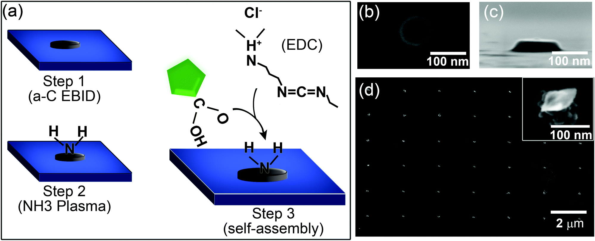 | ||
| Fig. 1 Self-assembly of nanodiamonds on electron beam deposited carbon seeds. (a) Schematic of the process. (b, c) Plan and side view SEM images of amorphous carbon disks deposited by EBID. (d) SEM image of patterned area after nanodiamond attachment. The inset in (d) is a high magnification SEM image of an EBID seed with attached nanodiamonds. | ||
To ascertain the nanodiamond attachment yield and selectivity of the technique, we employ confocal microscopy to obtain photoluminescence (PL) maps and spectra of the fabricated arrays. For the optical measurements, we employed a home built confocal microscope with a high numerical aperture objective (100×, 0.9 N.A), used for both excitation and collection of the emitted light. A 532 nm continuous wave laser was used for excitation, and all measurements were done at room temperature under ambient conditions. Fig. 2a shows a SEM image of a nanodiamond array and Fig. 2b shows a confocal map of the same array. The bright fluorescent spots correspond to the emission from nitrogen vacancy (NV−) defects in the nanodiamonds. Variations in PL intensity seen in Fig. 2b are caused primarily by the number of nanodiamonds attached to each carbon seed and variations in the number of NV centres within each nanodiamond. Fig. 2c is the histogram obtained from the confocal scan of Fig. 2b, representing the variation of fluorescence in a pattern produced with this method. Fig. 2d shows the spectrum recorded from each spot, demonstrating that 32 out of 35 locations have the characteristic emission from the NV− centres, equating to a 92% yield for the attachment process. Note that no nanodiamonds were attached in between the EBID seeds, giving the technique 100% selectivity.
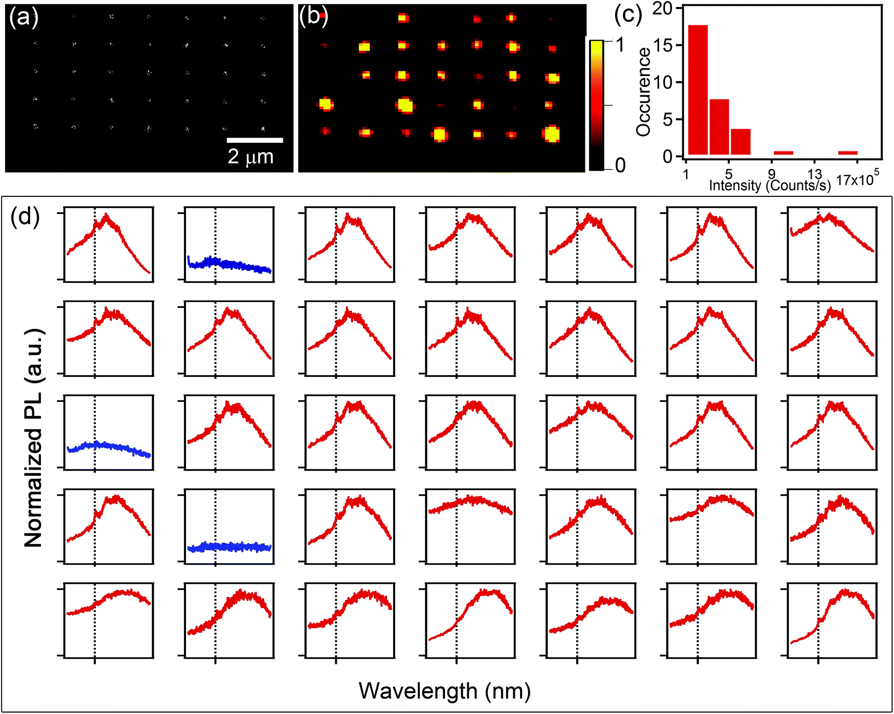 | ||
| Fig. 2 Characterization of attachment yield and selectivity. (a) SEM image of a nanodiamond pattern. (b) Colour-coded confocal photoluminescence map of the same nanodiamond pattern. (c) Histogram of the PL intensities from each spot in the confocal map. (d) Corresponding normalized PL spectra from each individual spot showing the NV− emission at 637 nm. The NV− zero phonon line is marked with a vertical dashed line for clarity. The adjacent broad emission is the phonon sideband. Only three locations in the patterned array do not show the NV− ZPL (blue curves). | ||
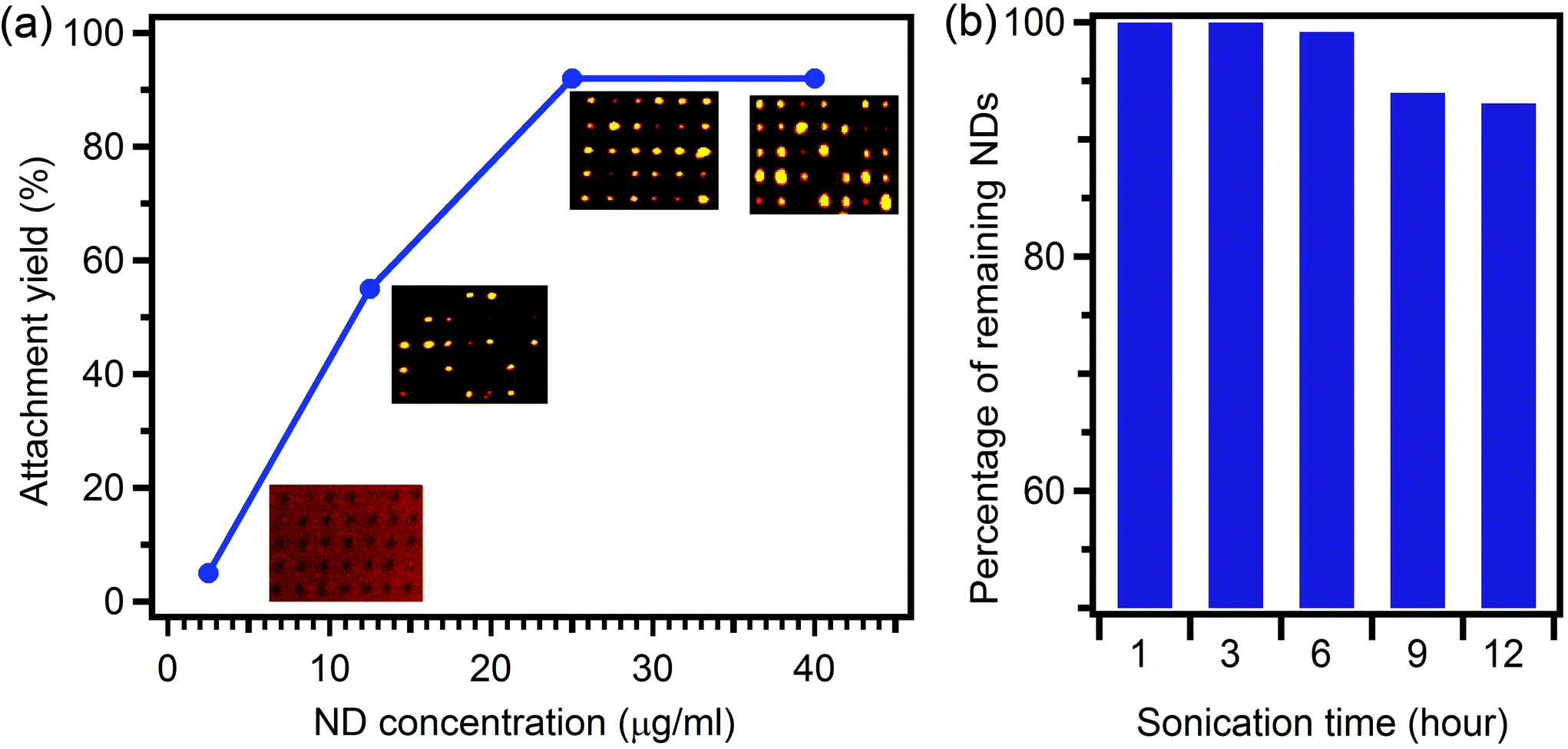
We now study the effect of the nanodiamond concentration on the attachment yield. Fig. 3a shows a clear dependence of the yield on the initial concentration of fluorescent nanodiamonds. Increasing the nanodiamond concentration results in improved attachment yield. At a nanodiamond concentration of 2.5 μg ml−1 the attachment yield was smaller than 5%, increasing to 50% at a concentration of 12.5 μg ml−1. The optimum concentration was found to be 25 μg ml−1, resulting in greater than 92% attachment, with only a few spots having no nanodiamonds. A higher concentration of nanodiamonds resulted in agglomeration with no increase in yield. The probabilities were deduced by analysis of confocal maps recorded under the same conditions as in Fig. 2 (and shown for each data point in Fig. 3). For all experiments, the ratio of EDC![[thin space (1/6-em)]](https://www.rsc.org/images/entities/char_2009.gif) :nanodiamonds in the solution was fixed at 10:1.
:nanodiamonds in the solution was fixed at 10:1.
 | ||
| Fig. 3 (a) Effect of nanodiamond concentration on the attachment yield. The yields were calculated from confocal maps shown next to each data point. (b) Robustness of nanodiamond array under sonication. | ||
The effectiveness of our method relies on covalent bonding between the amine and carboxyl functional groups on amorphous carbon and nanodiamond surfaces in the presence of EDC. We therefore expected the attached nanodiamonds to withstand further processing and treatment, as is required for many device applications. To examine the robustness of the technique, the assembled nanodiamonds were sonicated in a powerful ultrasonic bath (Bransonic 185 Watt Ultrasonic cleaner 221). Fig. 3b shows the remaining nanodiamonds after multi-step ultra-sonication for up to 12 hours. After three hours of sonication, all the nanodiamonds that were initially assembled were still attached to the substrate. Even after 12 hours, more than 90% of the self-assembled nanodiamonds remained on the surface, proving the unprecedented robustness of the assembly technique.
Finally, we demonstrate that the formed array can be used as a high-resolution magnetic field sensor, where each element in the array can serve as an individual pixel. Here, a microwave is guided through a 30 μm wire and the NV− spin states are read out optically (so-called optically detected magnetic resonance, ODMR, described in ESI S3†) (Fig. 4a).41 Such sensing of magnetic fields in ambient environments is one of the most prominent applications of the NV− centre. Fig. 4b shows a confocal map of the array of NV− centers. Fig. 4(c–e) shows three examples of optically detected magnetic resonance (ODMR) from randomly selected pixels in the array (marked with green circles). The red curves are nearly identical for all pixels and correspond to zero magnetic field. The green and the blue curves show the ODMR under 1 mT and 3 mT magnetic field. Each pixel shows a distinct ODMR signal that can then be used to deduce the local magnetic field in the proximity of the pixel. Note that since the measurement is done with an ensemble of nanodiamonds, the signal is broadened, with each dip comprising several lines from different NV− centers at each spot in the array. This technique is ideal to test for local absorption of metal nanoparticles or the presence of foreign para- and ferromagnetic metals. In principle, our technique can also be applied to nanodiamonds with single emitters, which are advantageous for quantum photonic applications.
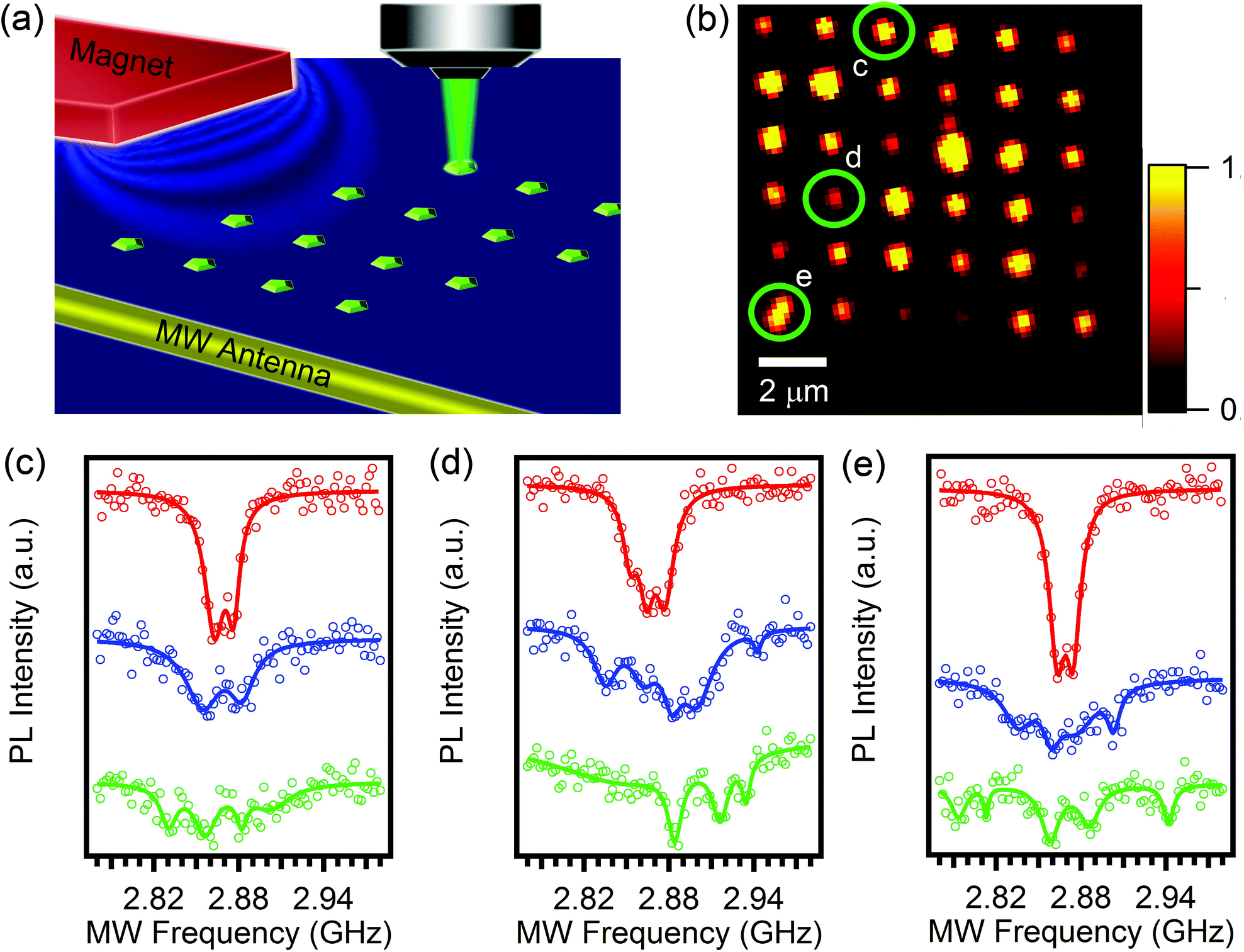 | ||
| Fig. 4 Demonstration of the nanodiamond array operating as a magnetic field sensor. (a) A microwave is guided through a 30 μm wire and electron spins are read out optically (b) confocal map of the nanodiamonds assembled into an array. (c–e) Optically detected magnetic resonance (ODMR) signal recorded from different elements (pixels) in the array – as shown by green circles. Red curve is ODMR under zero magnetic field while blue and green curves correspond to 1 and 3 mT fields, respectively. | ||
In conclusion we have developed a facile, generic technique for directed assembly of fluorescent nanodiamonds into robust arrays. The assembly technique has greater than 90 percent efficiency. Moreover, the nanodiamonds are covalently bonded and stay in their positions even after repeated ultrasonication treatments, making the technique very attractive for practical device applications. Finally, we have performed a proof of principle sensing measurement of various magnetic fields to show that each pixel in the array can be used as an independent magnetic field sensor. Larger nanoparticle arrays, as well as serial device production can, in principle, be achieved using a multibeam scanning electron microscope and thin passivation layers applied between sequential processing steps. Our method paves the way to realization of scalable platforms for sensing or integrated quantum photonics, where there is a real need for robust, large area assembly of fluorescent nanoparticles.
Author contributions
C. J. L. and S. J. R. conceived the idea, C. J. L., I. A., O. S., M. K., S. J. R. and M. T. designed the experiments, M. K. and A. B. conducted the experiments, A. W. S. contributed towards the ODMR measurements and C. J. L., I. A. and M. K. wrote the manuscript. All authors have discussed the results and given approval to the final version of the manuscript.Acknowledgements
This work was funded by FEI Company and the Australian Research Council. The authors thank Hugh Mackay for assistance with EBID seed fabrication.References
- S. Steinert, F. Dolde, P. Neumann, A. Aird, B. Naydenov, G. Balasubramanian, F. Jelezko and J. Wrachtrup, Rev. Sci. Instrum., 2010, 81(4), 043705 CrossRef CAS PubMed.
- Y. Wu, F. Jelezko, M. B. Plenio and T. Weil, Angew. Chem., Int. Ed., 2016, 55(23), 6586–6598 CrossRef CAS PubMed.
- C. Santori, P. E. Barclay, K. M. Fu, R. G. Beausoleil, S. Spillane and M. Fisch, Nanotechnology, 2010, 21(27), 274008 CrossRef CAS PubMed.
- G. D. Fuchs, G. Burkard, P. V. Klimov and D. D. Awschalom, Nat. Phys., 2011, 7(10), 789–793 CrossRef.
- L. Childress and R. Hanson, MRS Bull., 2013, 38(02), 134–138 CrossRef CAS.
- V. R. Manfrinato, D. D. Wanger, D. B. Strasfeld, H. S. Han, F. Marsili, J. P. Arrieta, T. S. Mentzel, M. G. Bawendi and K. K. Berggren, Nanotechnology, 2013, 24(12), 125302 CrossRef PubMed.
- W. Xie, R. Gomes, T. Aubert, S. Bisschop, Y. Zhu, Z. Hens, E. Brainis and D. Van Thourhout, Nano Lett., 2015, 15(11), 7481–7487 CrossRef CAS PubMed.
- Y. Wang, Y. Zhang, B. Li, J. Lü and J. Hu, Appl. Phys. Lett., 2007, 90(13), 133102 CrossRef.
- P. Maletinsky, S. Hong, M. S. Grinolds, B. Hausmann, M. D. Lukin, R. L. Walsworth, M. Loncar and A. Yacoby, Nat. Nanotechnol., 2012, 7(5), 320–324 CrossRef CAS PubMed.
- S. G. Rao, A. Karim, J. Schwartz, N. Antler, T. Schenkel and I. Siddiqi, ACS Appl. Mater. Interfaces, 2014, 6(15), 12893–12900 CAS.
- M. Jiang, J. A. Kurvits, Y. Lu, A. V. Nurmikko and R. Zia, Nano Lett., 2015, 15(8), 5010–5016 CrossRef CAS PubMed.
- M. Kolibal, M. Konecny, F. Ligmajer, D. Skoda, T. Vystavel, J. Zlamal, P. Varga and T. Sikola, ACS Nano, 2012, 6(11), 10098–10106 CrossRef CAS PubMed.
- A. Gopinath, E. Miyazono, A. Faraon and P. W. Rothemund, Nature, 2016, 535(7612), 401–405 CrossRef CAS PubMed.
- T. Zhang, A. Neumann, J. Lindlau, Y. Wu, G. Pramanik, B. Naydenov, F. Jelezko, F. Schuder, S. Huber, M. Huber, F. Stehr, A. Hogele, T. Weil and T. Liedl, J. Am. Chem. Soc., 2015, 137(31), 9776–9779 CrossRef CAS PubMed.
- P. Andrich, B. J. Aleman, J. C. Lee, K. Ohno, C. F. de las Casas, F. J. Heremans, E. L. Hu and D. D. Awschalom, Nano Lett., 2014, 14(9), 4959–4964 CrossRef CAS PubMed.
- S. Steinert, F. Ziem, L. T. Hall, A. Zappe, M. Schweikert, N. Gotz, A. Aird, G. Balasubramanian, L. Hollenberg and J. Wrachtrup, Nat. Commun., 2013, 4, 1607 CrossRef CAS PubMed.
- H. J. Mamin, M. Kim, M. H. Sherwood, C. T. Rettner, K. Ohno, D. D. Awschalom and D. Rugar, Science, 2013, 339(6119), 557–560 CrossRef CAS PubMed.
- T. Schroeder, A. W. Schell, G. Kewes, T. Aichele and O. Benson, Nano Lett., 2011, 11(1), 198–202 CrossRef PubMed.
- A. Huck, S. Kumar, A. Shakoor and U. L. Anderson, Phys. Rev. Lett., 2011, 106(9), 096801–096801 CrossRef PubMed.
- T. T. Tran, J. Fang, H. Zhang, P. Rath, K. Bray, R. G. Sandstrom, O. Shimoni, M. Toth and I. Aharonovich, Adv. Mater., 2015, 27(27), 4048–4053 CrossRef CAS PubMed.
- J. M. Taylor, P. Cappellaro, L. Childress, L. Jiang, D. Budker, P. R. Hemmer, A. Yacoby, R. Walsworth and M. D. Lukin, Nat. Phys., 2008, 4(10), 810–816 CrossRef CAS.
- S. Hong, M. S. Grinolds, L. M. Pham, D. Le Sage, L. Luan, R. L. Walsworth and A. Yacoby, MRS Bull., 2013, 38(02), 155–161 CrossRef CAS.
- J. P. Tetienne, A. Lombard, D. A. Simpson, C. Ritchie, J. Lu, P. Mulvaney and L. C. Hollenberg, Nano Lett., 2016, 16(1), 326–333 CrossRef CAS PubMed.
- G. Kucsko, P. C. Maurer, N. Y. Yao, M. Kubo, H. J. Noh, P. K. Lo, H. Park and M. D. Lukin, Nature, 2013, 500(7460), 54–58 CrossRef CAS PubMed.
- P. Neumann, I. Jakobi, F. Dolde, C. Burk, R. Reuter, G. Waldherr, J. Honert, T. Wolf, A. Brunner and J. H. Shim, Nano Lett., 2013, 13(6), 2738–2742 CrossRef CAS PubMed.
- L. P. McGuinness, Y. Yan, A. Stacey, D. A. Simpson, L. T. Hall, D. Maclaurin, S. Prawer, P. Mulvaney, J. Wrachtrup, F. Caruso, R. E. Scholten and L. C. Hollenberg, Nat. Nanotechnol., 2011, 6(6), 358–363 CrossRef CAS PubMed.
- A. W. Schell, G. Kewes, T. Hanke, A. Leitenstorfer, R. Bratschitsch, O. Benson and T. Aichele, Opt. Express, 2011, 19(8), 7914–7920 CrossRef CAS PubMed.
- O. Benson, Nature, 2011, 480(7376), 193–199 CrossRef CAS PubMed.
- O. Shimoni, J. Cervenka, T. J. Karle, K. Fox, B. C. Gibson, S. Tomljenovic-Hanic, A. D. Greentree and S. Prawer, ACS Appl. Mater. Interfaces, 2014, 6(11), 8894–8902 CAS.
- I. Aharonovich, J. C. Lee, A. P. Magyar, D. O. Bracher and E. L. Hu, Laser Photonics Rev., 2013, 7(5), L61–L65 CrossRef CAS.
- R. W. Heeres, L. P. Kouwenhoven and V. Zwiller, Nat. Nanotechnol., 2013, 8(10), 719–722 CrossRef CAS PubMed.
- M.-C. Dheur, E. Devaux, T. W. Ebbesen, A. Baron, J.-C. Rodier, J.-P. Hugonin, P. Lalanne, J.-J. Greffet, G. Messin and F. Marquier, Sci. Adv., 2016, 2, e1501574 Search PubMed.
- F. Liu, E. J. Luber, L. A. Huck, B. C. Olsen and J. M. Buriak, ACS Nano, 2015, 9, 2184–2193 CrossRef CAS PubMed.
- I. Utke, P. Hoffmann and J. Melngailis, J. Vac. Sci. Technol., B: Microelectron. Nanometer Struct. – Process., Meas., Phenom., 2008, 26(4), 1197 CrossRef CAS.
- C. J. Lobo, A. Martin, M. R. Phillips and M. Toth, Nanotechnology, 2012, 23(37), 375302 CrossRef PubMed.
- M. L. Steen, K. R. Kull and E. R. Fisher, J. Appl. Phys., 2002, 92(1), 55 CrossRef CAS.
- Y. Liang, M. Ozawa and A. Krueger, ACS Nano, 2009, 3(8), 2288–2296 CrossRef CAS PubMed.
- A. Krüger, Y. Liang, G. Jarre and J. Stegk, J. Mater. Chem., 2006, 16(24), 2322–2328 RSC.
- S.-J. Yu, M.-W. Kang, H.-C. Chang, K.-M. Chen and Y.-C. Yu, J. Am. Chem. Soc., 2005, 127(50), 17604–17605 CrossRef CAS PubMed.
- M. Montalti, A. Cantelli and G. Battistelli, Chem. Soc. Rev., 2015, 44(14), 4853–4921 RSC.
- A. Gruber, A. Dräbenstedt, C. Tietz, L. Fleury, J. Wrachtrup and C. V. Borczyskowski, Science, 1997, 276(5321), 2012–2014 CrossRef CAS.
Footnote |
| † Electronic supplementary information (ESI) available. See DOI: 10.1039/c6nr05419f |
| This journal is © The Royal Society of Chemistry 2016 |