
 Open Access Article
 This Open Access Article is licensed under a
 Creative Commons Attribution 3.0 Unported Licence
Strongly polarized quantum-dot-like light emitters embedded in GaAs/GaNAs core/shell nanowires†
S.
Filippov‡
a,
M.
Jansson‡
a,
J. E.
Stehr
a,
J.
Palisaitis
a,
P. O. Å.
Persson
a,
F.
Ishikawa
b,
W. M.
Chen
a and
I. A.
Buyanova
 *a
*a
aDepartment of Physics, Chemistry and Biology, Linköping University, 58183 Linköping, Sweden. E-mail: iribu@ifm.liu.se
bGraduate School of Science and Engineering, Ehime University, 790-8577 Matsuyama, Japan
First published on 1st August 2016
Abstract
Recent developments in fabrication techniques and extensive investigations of the physical properties of III–V semiconductor nanowires (NWs), such as GaAs NWs, have demonstrated their potential for a multitude of advanced electronic and photonics applications. Alloying of GaAs with nitrogen can further enhance the performance and extend the device functionality via intentional defects and heterostructure engineering in GaNAs and GaAs/GaNAs coaxial NWs. In this work, it is shown that incorporation of nitrogen in GaAs NWs leads to formation of three-dimensional confining potentials caused by short-range fluctuations in the nitrogen composition, which are superimposed on long-range alloy disorder. The resulting localized states exhibit a quantum-dot like electronic structure, forming optically active states in the GaNAs shell. By directly correlating the structural and optical properties of individual NWs, it is also shown that formation of the localized states is efficient in pure zinc-blende wires and is further facilitated by structural polymorphism. The light emission from these localized states is found to be spectrally narrow (∼50–130 μeV) and is highly polarized (up to 100%) with the preferable polarization direction orthogonal to the NW axis, suggesting a preferential orientation of the localization potential. These properties of self-assembled nano-emitters embedded in the GaNAs-based nanowire structures may be attractive for potential optoelectronic applications.
Introduction
Group III–V semiconductor nanowires (NWs) have emerged within recent years as promising building blocks for a wide variety of advanced applications in electronics, sensing, optoelectronics, etc.1,2 These structures combine all of the advantages of III–V semiconductors, including a direct bandgap, high carrier mobility, and advanced bandgap engineering, with those offered by the one-dimensional (1D) geometry such as efficient lateral strain relaxation, photonic confinement and possible quantum confinement effects. The latter effects can be utilized in sufficiently thin wires with diameters smaller than the electron Bohr radius, which can be a challenging task from growth perspectives and also because of surface recombination that is known to be particularly severe in III–V materials. An attractive alternative fabrication approach includes synthesis of multi-shell heterostructures with embedded 1D quantum wires or zero-dimensional (0D) quantum dots (QDs).3–17 Achieving the strong confinement limit in such hybrid QD-NW systems can lead to substantial performance improvements in the characteristics of advanced nano-emitters and third-generation solar cells.11,15 Ultimately, it will allow realization of single photon emissions,4,7,8 single-spin detection,13 single-shot electrical readout3 and generation of entangled photon pairs,12 which can pave the way for innovative applications of nanowires in quantum photonics and quantum information technologies. So far the formation of QDs embedded in NW structures has been investigated with the focus on conventional III–V material systems of GaAs/AlGaAs,5,6 GaAs/GaAsP,4,17 InAsP/InP8,12 and In(Ga)As/GaAs.7,11 In addition to deliberate lateral confinement in axial heterostructures,4,12,13 the QD formation was also found to occur because of polymorphism in the axial direction,18 random alloy fluctuations,5 as well as formation of Al-rich islands at the apex of GaAs/AlGaAs interfaces in <111>-grown wires.9,15Among the promising material systems for optoelectronic applications are Ga(In)NAs alloys, which belong to the so-called dilute nitride semiconductor family.19 Substituting a small fraction of As atoms with N has been shown to drastically change the electronic structure of the resulting alloys, leading to the huge bandgap bowing20 and, thus, the possibility to tune the bandgap energy down to 1.3 and 1.55 μm that are utilized for fiber-optic communications. The N-induced splitting of conduction band (CB) states also provides the possibility to realize third-generation intermediate-band solar cells with envisioned record efficiencies.21,22 Furthermore, by exploiting spin-dependent carrier recombination processes in dilute nitrides, these materials have shown extraordinary spin properties and great promise for room-temperature spin filters, spin detectors, spin amplifiers, and nuclear spin polarization enablers, with record efficiencies23–25 that do not require an application of an external magnetic field. Additionally, doping of bulk GaAs and thin films by nitrogen is known to lead to formation of strongly localized states that can act as single photon emitters26 and exciton qubits.27 For very low N compositions that are within the doping limit, the localized states originate from N-related clusters.28–31 With increasing N compositions above the doping limit, on the other hand, the localized states are caused by short- and long-range potential fluctuations in the bandgap energy due to alloy disorder32,33 that is amplified in the N-containing alloys because of the giant bandgap bowing effect.20
Most recently GaNAs alloys with superior optical quality were grown in 1D geometry as a shell layer in GaAs/GaNAs core/shell NWs,34–36 providing the opportunity to combine the attractive physical properties of the GaNAs alloy with advantages offered by the NW architecture. The presence of nitrogen in such NW structures was shown to be advantageous for improving their radiative efficiency as compared with N-free GaAs wires, likely due to suppression of surface recombination caused by N-assisted surface passivation.37 This behavior is in stark contrast to bulk dilute nitrides, where alloying with nitrogen degrades the optical quality of the material due to the formation of non-radiative recombination centers.38–40 In this work we show that alloying with nitrogen can also lead to the formation of self-assembled nano-emitters embedded in the GaNAs-based nanowire structures. Specifically, it is found that local fluctuations in the N composition inside such coaxial GaAs/GaNAs NWs induces three-dimensional confining potentials equivalent to that for QDs. This results in optically active and highly localized states inside the GaNAs shell. By directly correlating structural and optical properties of individual NWs, we reveal that the formation of these states (referred to below as QD-like states) is efficient in pure zinc-blende (ZB) wires and is further facilitated by structural polymorphism. The emission from these self-assembled QD-like states is found to be spectrally narrow [with a full-width-at-half-maximum (FWHM) ranging between 50 and 130 μeV] and highly polarized (up to 100%).
Results and discussion
The investigated GaAs and GaAs/GaN0.005As0.995 core/shell NWs were grown by plasma-assisted molecular beam epitaxy (MBE) on (111) Si substrates using Ga droplets as a catalyst (see the Experimental section for a detailed description of the NW growth). As a reference, we also grew GaAs/GaAs NW structures (referred below as GaAs NWs) that were produced under identical conditions as the GaAs/GaNAs NWs but without N doping. All investigated NWs are on average ∼4 μm long, with a total diameter of 300 nm and a thickness of about 100 nm for the Ga(N)As shell layer.35 The structural properties of these NWs were investigated by transmission electron microscopy (TEM). Representative TEM images are shown in Fig. 1, where Fig. 1a and e depict an overview of the TEM images of a GaAs NW and a GaAs/GaNAs core/shell NW, respectively. They predominantly crystalize in the ZB structure and exhibit a few structural defects within the first 1–2 μm, where the density of randomly nucleated twin planes formed perpendicular to the NW growth axis is below 5 twins per micron. The corresponding areas are labelled as ZB in Fig. 1a and e with the twin positions being marked by the arrows. The twin density progressively increases towards the top part of the NWs [labeled as the twinned ZB (tZB) in Fig. 1]. These polymorphic regions (referred to as the “mixed” regions, for simplicity) may also contain wurtzite (WZ) segments, which are usually rather short and do not exceed 200 nm in length. The total contribution of the WZ phase is found to be below 5% of the NW volume. High resolution TEM (HR-TEM) images of the pure ZB, WZ and twinned ZB areas are shown in Fig. 1b–d and f–h for the GaAs and GaAs/GaNAs core/shell NWs, respectively. From Fig. 1, we also note that the presence of nitrogen does not affect the structural quality of the wires.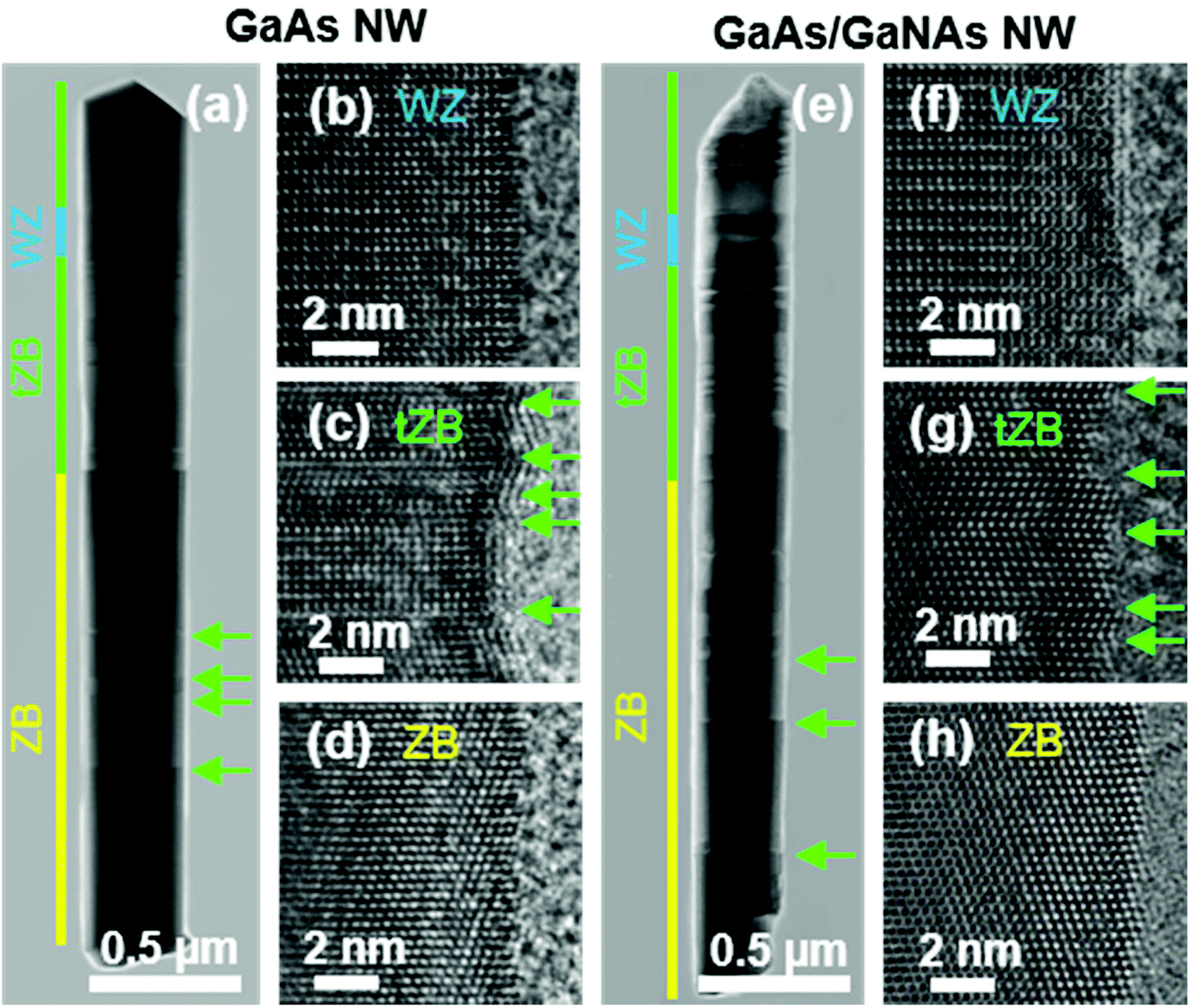 | ||
| Fig. 1 TEM images of the representative NWs. (a) and (e) are the overview images of a GaAs NW and a GaAs/GaN0.005As0.995 NW, respectively. The yellow, green and blue bars mark the nanowire segments with pure ZB, tZB and WZ lattice structures, respectively. (b–d) and (f–h) show HR-TEM images of the specified areas of the GaAs NW and GaAs/GaNAs NW, respectively. The green horizontal arrows indicate the positions of the rotational twin planes within the ZB regions. The twin positions are not marked in (a) and (e) within the tZB segments due to a high density, but are indicated in the HR-TEM images shown in (c) and (g). | ||
In order to elucidate the impact of the crystal structure on optical properties, we performed μ-photoluminescence (μ-PL) measurements on the same wires as those characterized by TEM. For each NW, the measurements were performed by selectively exciting either the pure ZB or the mixed regions. The corresponding results are summarized in Fig. 2, which show typical μ-PL spectra measured at 4.4 K from a single GaAs NW (a) and a single GaAs/GaNAs NW (b), respectively. The PL spectra of the reference GaAs NWs are consistent with those previously reported in the literature.18,41–49 Within the pure ZB part (i.e. the ZB region of the wire with only a few twins), the PL emission is dominated by the free exciton (FX) transition at 1.515 eV – see Fig. 2a. Besides the FX feature, the PL spectra contain several PL lines peaking at around 1.494, 1.488 and 1.476 eV. The former two emissions likely originate from impurities and could be attributed to conduction-band-acceptor and donor–acceptor pair transitions involving residual acceptor impurities.50–52 The 1.476 eV line is related to the presence of the twins within the ZB region,49 which is enhanced in the mixed regions with a higher density of the twins as seen from the TEM images shown in Fig. 1a and e. Additionally, the PL spectra contain a series of lines within the spectral range of 1.44–1.47 eV that were previously shown to originate from type-II transitions at boundaries between the WZ and ZB phases and at stacking faults.18,41–49
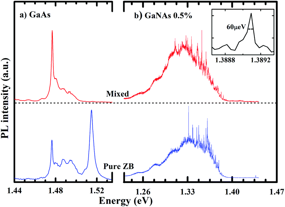 | ||
| Fig. 2 Representative PL spectra measured from the pure ZB and the mixed regions of the GaAs (a) and GaAs/GaN0.005As0.995 NWs (b) shown in Fig. 1. The GaAs/GaNAs NW PL spectra contain numerous sharp lines superimposed with a broad background due to the LE emission. The inset in (b) shows a magnified part of the spectrum from the GaAs/GaN0.005As0.995 NW. | ||
The presence of the GaNAs shell results in a significant modification of the μ-PL spectra – see Fig. 2b. The overall PL spectra shift towards lower energies to a degree determined by nitrogen compositions in the shell, whereas the core emissions within the 1.44–1.52 eV spectral range are quenched. The observed changes reflect the formation of the GaNAs alloy and the fact that the monitored radiative recombination in the GaAs/GaNAs core/shell NWs predominantly occurs within the GaNAs shell with a smaller bandgap.36 Trapping of the photo-generated carriers within the GaNAs shell is facilitated by the type-I band alignment between GaNAs and GaAs.19 The PL spectra from both pure ZB and mixed regions of the wire consist of a series of sharp lines superimposed on a broad PL band. The origin of the latter was studied in detail in our previous work based on temperature-dependent, continuous-wave and transient PL measurements.36 This emission, which exhibits a gradual red shift with increasing nitrogen composition, was shown to arise from the recombination of weakly localized excitons (LE) trapped by potential fluctuations induced by long-range fluctuations of the nitrogen composition in the GaNAs shell. The spectral position of the LE band practically remains constant throughout the wire, which implies a rather uniform average nitrogen composition and alloy disorder within the wire.36 On the other hand, the appearance of the sharp lines is strongly spot-dependent (see the ESI†). Combined with the extremely narrow linewidth of these transitions, with a FWHM of 50–130 μeV – see the inset in Fig. 2(b), these sharp lines can be attributed to the optical transitions associated with strongly localized, e.g. QD-like, states that are randomly but not uniformly distributed within the wire. The observed large number (more than 100) of the sharp lines indicates a large number of independent light emitters within the excitation volume, setting the upper bound of the size of the confinement potentials to be much less than 60 nm. Their formation seems to be more probable within the mixed regions, as the number of the sharp lines in these areas is about 50% higher than that in the pure ZB segments of the nanowires. The localization cannot simply be caused by carrier confinement in narrow WZ/ZB segments within the polymorphic region of the GaNAs shell, however, as intense narrow lines can also be detected from the pure ZB regions. On the other hand, their appearance is undoubtedly related to the presence of nitrogen, since they can only be detected in the GaAs/GaNAs NWs with [N] = 0.5% and [N] = 0.1% (see the ESI†). None of these lines could be detected from the pure GaAs NWs. Moreover, trapping of the photo-excited carriers to these highly localized states primarily occurs via carrier/exciton supply from extended states within the GaNAs shell. This can be clearly seen from the results of performed PL excitation (PLE) measurements when the PL intensity of individual sharp lines is recorded while tuning the energy of the excitation laser – see Fig. 3. The PLE spectra from all sharp lines with similar photon energies are nearly identical, within the experimental accuracy, and exhibit the same onset of the PLE spectra. Since the same onset was also found in the PLE spectra of the LE background emission from the weakly localized excitons, it can be concluded that this onset corresponds to the GaNAs bandgap energy.36 These facts suggest that the deeply localized states are formed within the GaNAs shell layer.
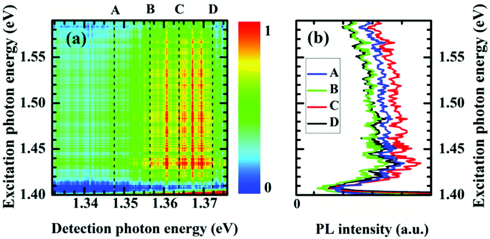 | ||
| Fig. 3 μ-PL intensity as a function of both detection and excitation energy from the GaAs/GaNAs core/shell NW structure. (b) μ-PLE spectra measured from several QD-like PL emission lines marked in (a). | ||
Possible sources of the nanoscale confinement potentials could be defects and true quantum confinement due to bandgap modifications. For example, various N-related clusters, which contain several nitrogen atoms, are known26–31 to introduce a range of deep levels within the GaNAs bandgap (determined by the number and mutual arrangement of the involved N atoms). We note, however, that the ultra-narrow PL lines from the N cluster bound excitons in bulk GaAs were so far detected only at substantially higher energies within the range of 1.443–1.5 eV,26–31 making this scenario somewhat less likely. An alternative candidate arises from excitons trapped within local potentials by random local fluctuations in the nitrogen composition. In GaNAs, the conduction band edge downshifts with increasing N content whereas the valence band shifts upwards, leading to type-I band line-up between the regions with a locally higher/lower N content.19,53,54 Therefore, short-range fluctuations in the N content can create a 3D confinement potential within some regions of the nanowires and act as quantum dots. This model is consistent with our results of PL transient measurements,37 which have shown that the radiative lifetime of the strongly localized excitons in GaNAs is comparable to that in GaAs and is temperature-independent.
To gain insight into the spatial locations of these QD-like emitters, PL measurements were performed with different excitation wavelengths and, thus, different penetration depths of the excitation light. The corresponding results acquired from the same single NW with excitation photon wavelengths in the range of 800–445 nm (1.55–2.79 eV) are shown in Fig. 4a. From Fig. 3a and 4a it is apparent that the changes of the excitation photon energy between 2.8 and 1.4 eV do not affect either the number of the sharp lines or the relative intensity between these sharp lines and the broad background LE emission. This can also be seen from Fig. 4c, which exhibits a nearly constant ratio R between integrated intensity from all sharp lines (Ilines) and the intensity of the broad background (IBG), R = ILines/IBG. Since the penetration depths of the excitation light under such conditions (indicated by the arrows in Fig. 4b) change from ∼70 nm to more than 400 nm,55 the states giving rise to the sharp lines are most likely located within the bulk regions of the shell layer (i.e. not surface-related).
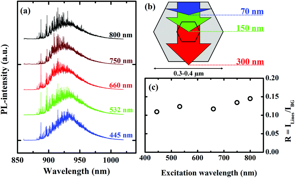 | ||
| Fig. 4 (a) PL spectra measured from the same single NW with the excitation wavelengths as specified in the figure. (b) The penetration depth of the laser light estimated using the absorption coefficient from ref. 55. (c) The ratio R of the integrated intensity of the sharp PL lines and the broad background LE emission. | ||
To gain further information on the electronic structure of these states, we performed a series of detailed polarization-resolved μ-PL studies of individual lines. Since the broad PL background from the LE may mask the actual polarization degrees of the sharp lines, it was first subtracted from the PL spectra. Representative dependences of the PL intensity as a function of the detection energy and the angle, and the corresponding angular plots are shown in Fig. 5a–c and d–f, respectively. The angular variation of the PL intensity from each individual line can be fitted with the expression
| I = Iminsin2(ϕ − θ) + Imaxcos2(ϕ − θ) | (1) |
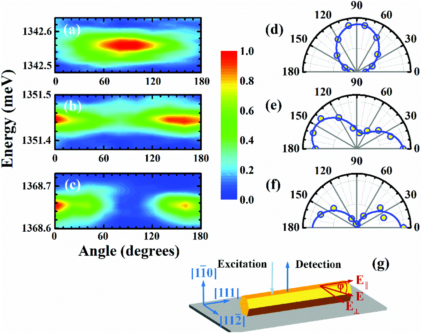 | ||
| Fig. 5 (a)–(c) 2D color plots of the PL intensity as a function of the detection energy and the angle ϕ for several representative PL lines. (d)–(f) The corresponding polar plots of the PL intensity. The solid lines are the simulated curves obtained by eqn (1). The angles are measured relatively to the NW axis. (g) Schematic illustrating the measurement geometry used for polarization resolved μ-PL measurements. E is the polarization direction of the analyzer rotated by the angle ϕ relative to the nanowire axis. Its components, which are parallel and perpendicular to the NW axis, are given by E|| and E⊥, respectively. | ||
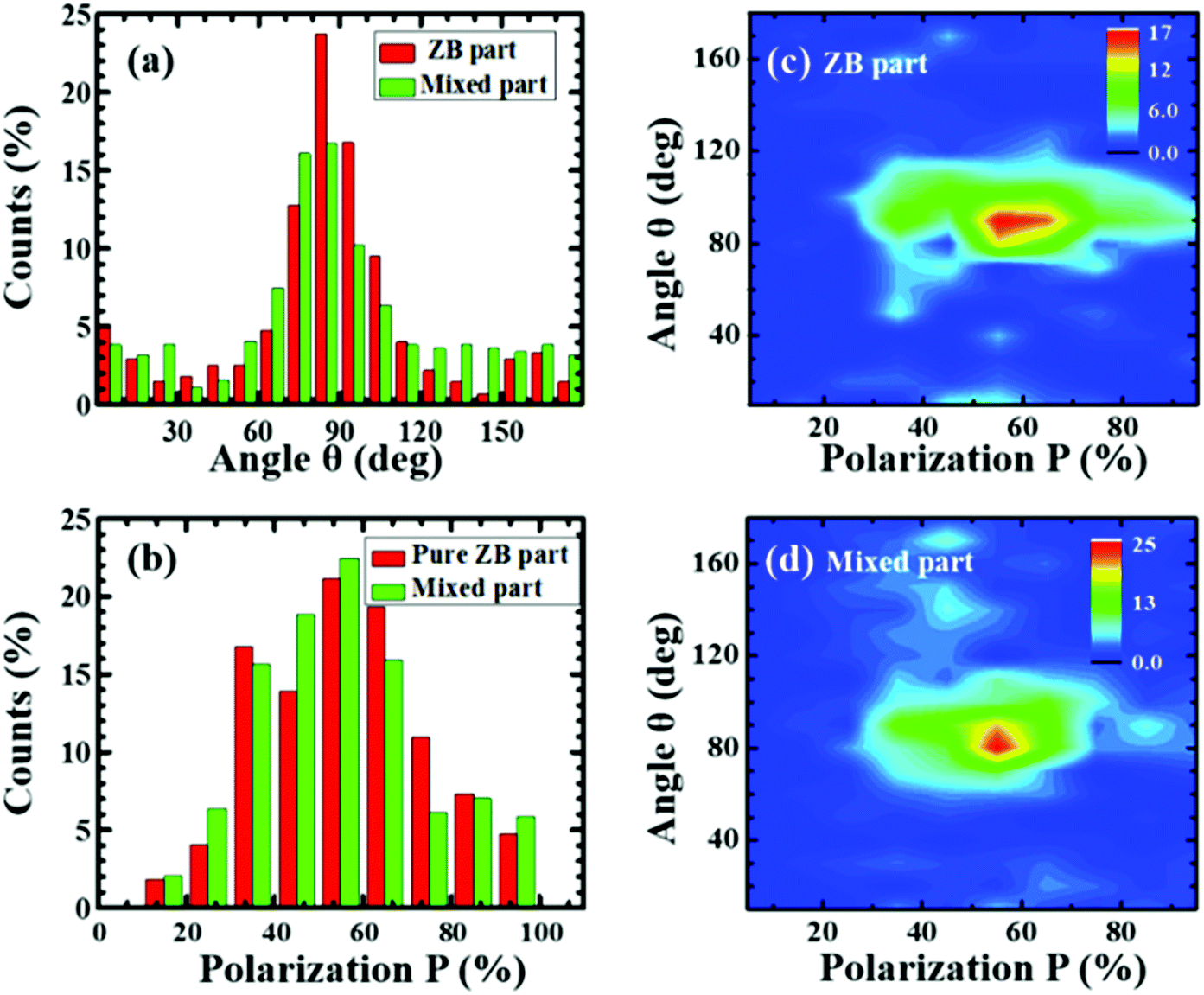 | ||
| Fig. 6 Statistical distributions of the angle θ of the polarization axis (a) and the polarization degree P (b) measured from the ZB (red) and the mixed (green) regions of the studied GaAs/GaNAs NW structures. (c) and (d) show the number of PL lines as a function of both angle θ and polarization degree P measured from the ZB and mixed regions, respectively. The total numbers of the QD-like emission lines used in the statistical distributions are 274 and 442 for the ZB and the mixed regions, respectively. | ||
The observed preferentially orthogonal polarization of the QD-like emissions can only be explained by assuming that the main quantization direction of the excitons giving rise to the emissions coincides with the [111] NW axis. Indeed, the electronic structure of a neutral exciton confined in QDs that consist of an s-electron (Se = 1/2) and a p-hole (Jh = 3/2) is determined by a combined effect of exchange interaction and heave-hole–light-hole (hh–lh) splitting driven by a local strain field or/and directional quantum confinement that reduces symmetry. The exchange interaction promoted by a strong overlap between electron and hole wavefunctions in QDs will cause splitting of the excitonic state (Γ6 × Γ8 in ZB) into the bright (J = 1 triplet) and dark (J = 2 quintet) states. An anisotropy in the strain field and QD shape (and the crystal field in the WZ regions) will further lift their degeneracy between the hh and lh exciton states and will mix the bright and dark states, increasing the number of optically allowed transitions to a degree determined by the overall symmetry of the confinement potential. The optical polarization directions of these excitons are determined by the principal axes of the confinement potential as a result of the combined effect of the strain field and the QD shape.
The observed orthogonal polarization of light emission (i.e. θ around 90°) in our NWs implies that the predominant quantization axis of the QDs coincides with the NW axis. This preferential alignment can be caused by shear strain in the GaNAs shell created due to the lattice mismatch with the GaAs core layer that has a larger lattice constant. Indeed, as it was demonstrated in previous studies,58–60 overall uniaxial anisotropy of nanowires has significant effects on strain in coherent core/shell structures from lattice mismatched semiconductors. In addition to the hydrostatic component, the predominant strain contribution was found to arise from the axial εzz component. This will elongate the exciton confinement potential along the NW axis and will cause splitting between hh and lh valence band states at the Γ point with hh states being the ground state, due to a predominantly uniaxial tensile strain field in the GaNAs shell. This splitting will be further increased due to quantum confinement effects (and the crystal field in the WZ regions) along the same direction. The expected values of the PL polarization would then range between 100% (if the monitored emission is due to the recombination of hh excitons alone and the hh states retain a pure character) and 33% (if both hh and lh states are equally populated or the hh–lh splitting is smaller than the PL linewidth). As can be seen from Fig. 6, the majority of the monitored sharp lines have P > 33%, which means that the hh-states are preferentially populated. Fluctuations in the nitrogen composition will likely affect the strain distribution causing some tilting of the local strain field away from the NW axis. This will cause mixing between the hh and lh states, to a degree determined by the electronic structure of a particular dot, which will decrease the measured values of P from 100%. If the splitting between the hh and lh states exceeds the PL linewidth, the population of lh states will lead to the appearance of the emission lines that are polarized along the nanowire (i.e. with θ close to 0°), as is indeed observed experimentally. From Fig. 6a, some of the QDs have their principal axis also oriented in random directions. A similar behavior was also observed in self-assembled QDs embedded in GaAs/AlGaAs core/shell NWs5,15 and was attributed to surface effects. We note that the suggested exciton localization within the QD states is also consistent with the results of the performed power-dependent PL measurements (see the ESI†), which imply formation of biexcitons at a high excitation power level that is typical of QD systems.61–63
Conclusions
In conclusion, we have performed correlative studies by spatially resolved structural TEM and μ-PL to elucidate the effects of crystal structure and alloying with nitrogen on the optical properties of GaAs/GaNAs core/shell NWs grown by MBE on Si substrates. We showed that N incorporation leads to the appearance of numerous sharp emission lines with FWHM ranging between 50 μeV and 130 μeV, indicative for strong exciton confinement. The confining potential was suggested to be caused by local variations in the N composition [N] that are superimposed on long-range alloy disorder within the GaNAs shell. These local variations in [N] were promoted in the polymorphic areas with the mixed WZ/ZB crystal structure and a high density of rotational twins. Based on the performed detailed polarization resolved μ-PL studies, the most probable orientation of the principal quantization axis of these localized QD-like states is found to coincide with the direction of the NW axis. This gives rise to strong orthogonal polarization of the monitored PL lines, due to a predominantly uniaxial tensile strain field in the GaNAs shell, which is 50–60% on average but can reach up to 100%. Our results, therefore, show that alloying of GaAs with nitrogen is an efficient way to fabricate hybrid QD-NW structures with high crystalline and optical quality. The excitons confined in such novel hybrid structures may be found attractive for future applications as efficient nanoscale polarized-light sources that emit light within the near-infrared spectral range relevant to fiber-optic communications. Efforts aiming at designing strategies for deliberate formation of such QD emitters during the growth, such as those reported for the Ga(Al)As QDs,15,64 are currently under way.Experimental details
The investigated GaAs and GaAs/GaNAs core/shell NWs were grown by plasma-assisted MBE on (111) Si substrates using Ga droplets as a catalyst. The nitrogen composition in the shell layer was varied between 0.1 and 0.5%. The substrate was preheated to 570 °C under an As4 beam at an equivalent pressure of 1 × 10⁻⁵ Torr. The formation of the GaAs nanowire core was first achieved via constituent Ga-induced vapor–liquid–solid growth. The Ga supply was set to match a planar growth rate of 1.0 ML per s on (001) GaAs. The GaAs core was grown for 15 min at the requisite temperature to initiate longitudinal wire growth. Next, the growth was interrupted for 15 min and the equivalent pressure of the As4 beam was increased to 5 × 10⁻⁵ Torr to induce crystallization of the Ga catalyst on the tip of the NWs. After crystallization of the catalyst the lateral growth became dominant, which allowed formation of core–shell structures with precisely controlled shell diameters.34,35,65–67 The Ga flux was further supplied for 15 min to continue the radial growth of the GaAs core to the total thickness of 100 nm as was cross-checked from TEM measurements. During this time the substrate temperature was lowered down to 430 °C, to improve efficiency of the N incorporation during the subsequent growth of a GaNAs shell.35 The latter was performed for 30 min with an N plasma ignited and having flux of active nitrogen set to 3.5 × 10⁻³ ML per s. The so-produced GaNAs shell has a thickness of 100 nm.35 Cross-sectional TEM images of the GaAs/GaNAs core/shell NWs can be found in ref. 34. As a reference, we also grew GaAs/GaAs NW structures that were produced under the identical conditions as the GaAs/GaNAs NWs but without N flux irradiation.In order to conduct correlative structural and optical characterization, the NWs were mechanically transferred onto a carbon/copper TEM grid. The crystal structure of the NWs was analysed by recording high-resolution TEM images using a FEI Tecnai G2 TF 20 UT and the double-corrected Linkoping FEI Titan3 60-300 (operated at 300 keV) microscopes. During μ-PL measurements, the same transferred NWs were loaded into a cold-finger Oxford cryostat mounted on a custom-made X–Y stage. The measurements were performed at 4.4 K under the 659.32 nm excitation of a solid state laser in a backscattering geometry. The excitation and detection beams were focused and collected by a 50× Olympus objective lens with a numerical aperture NA = 0.5, resulting in a laser spot of ∼800–1000 nm in diameter. The excitation beam was focused close to the NW ends (within 0.5 μm) to ensure preferential excitation of either ZB or mixed regions. The excitation power was kept in the order of several tens of nW, to avoid sample heating and state filling effects. For optical polarization studies, a linear-polarization analyzer, consisting of a rotatable half-wave-plate in conjunction with a fixed Glan–Thompson linear polarizer, was placed in the detection path before the entrance slit of the spectrometer. The polarization optics was achromatic in the measurement range. The μ-PLE measurements were conducted with a tunable Ti:sapphire laser. The PL signal was dispersed by a high-resolution spectrometer, with a spectral resolution of about 5 μeV, and detected by a Peltier-cooled Si charge-coupled-device (CCD) detector. The polarization studies were performed on 5 nanowires that were characterized by TEM.
Acknowledgements
Financial support by the Swedish Energy Agency (grant # P40119-1) and the Swedish Research Council (grants # 2015-05532 and 2008-405) is greatly appreciated. The Knut and Alice Wallenberg Foundation is gratefully acknowledged for support of the Electron Microscopy laboratory in Linköping.References
- Y. Li, F. Qian, J. Xiang and C. M. Lieber, Mater. Today, 2006, 9, 18 CrossRef CAS.
- R. Yan, D. Gargas and P. Yang, Nat. Photonics, 2009, 3, 569 CrossRef CAS.
- G. Bulgarini, M. E. Reimer, M. Hocevar, E. P. A. M. Bakkers, L. P. Kouwenhoven and V. Zwiller, Nat. Photonics, 2012, 6, 455 CrossRef CAS.
- M. T. Borgström, V. Zwiller, E. Müller and A. Imamoglu, Nano Lett., 2005, 5, 1439 CrossRef.
- N. Jeon, B. Loitsch, S. Morkoetter, G. Abstreiter, J. Finley, H. J. Krenner, G. Koblmueller and L. J. Lauhon, ACS Nano, 2015, 9, 8335 CrossRef CAS PubMed.
- B. Loitsch, J. Winnerl, G. Grimaldi, J. Wierzbowski, D. Rudolph, S. Morkötter, M. Döblinger, G. Abstreiter, G. Koblmüller and J. J. Finley, Nano Lett., 2015, 15, 7544 CrossRef CAS PubMed.
- G. Sallen, A. Tribu, T. Aichele, R. André, L. Besombes, C. Bougerol, M. Richard, S. Tatarenko, K. Kheng and J.-P. Poizat, Nat. Photonics, 2010, 4, 174 CrossRef.
- E. D. Minot, F. Kelkensberg, M. Van Kouwen, J. A. V. Dam, L. P. Kouwenhoven, V. Zwiller, M. T. Borgström, O. Wunnicke, M. A. Verheijen and E. P. a. M. Bakkers, Nano Lett., 2007, 7, 367 CrossRef CAS PubMed.
- D. Rudolph, S. Funk, M. Döblinger, S. Morkötter, S. Hertenberger, L. Schweickert, J. Becker, S. Matich, M. Bichler, D. Spirkoska, I. Zardo, J. J. Finley, G. Abstreiter and G. Koblmüller, Nano Lett., 2013, 13, 1522 CrossRef CAS PubMed.
- T. Shi, H. E. Jackson, L. M. Smith, N. Jiang, Q. Gao, H. H. Tan, C. Jagadish, C. Zheng and J. Etheridge, Nano Lett., 2015, 15, 1876 CrossRef CAS PubMed.
- J. Tatebayashi, S. Kako, J. Ho, Y. Ota, S. Iwamoto and Y. Arakawa, Nat. Photonics, 2015, 9, 501 CrossRef CAS.
- M. A. M. Versteegh, M. E. Reimer, K. D. Jöns, D. Dalacu, P. J. Poole, A. Gulinatti, A. Giudice and V. Zwiller, Nat. Commun., 2014, 5, 5298 CrossRef CAS PubMed.
- M. H. M. van Weert, N. Akopian, U. Perinetti, M. P. van Kouwen, R. E. Algra, M. A. Verheijen, E. P. A. M. Bakkers, L. P. Kouwenhoven and V. Zwiller, Nano Lett., 2009, 9, 1989 CrossRef CAS PubMed.
- M. Weiß, J. B. Kinzel, F. J. R. Schülein, M. Heigl, D. Rudolph, S. Morkötter, M. Döblinger, M. Bichler, G. Abstreiter, J. J. Finley, G. Koblmüller, A. Wixforth and H. J. Krenner, Nano Lett., 2014, 14, 2256 CrossRef PubMed.
- M. Heiss, Y. Fontana, A. Gustafsson, G. Wüst, C. Magen, D. D. O'Regan, J. W. Luo, B. Ketterer, S. Conesa-Boj, A. V. Kuhlmann, J. Houel, E. Russo-Averchi, J. R. Morante, M. Cantoni, N. Marzari, J. Arbiol, A. Zunger, R. J. Warburton and A. Fontcuberta i Morral, Nat. Mater., 2013, 12, 439 CrossRef CAS PubMed.
- G. Priante, G. Patriarche, F. Oehler, F. Glas and J.-C. Harmand, Nano Lett., 2015, 15, 6036 CrossRef CAS PubMed.
- J. Wu, A. Ramsay, A. Sanchez, Y. Zhang, D. Kim, F. Brossard, X. Hu, M. Benamara, M. E. Ware, Y. I. Mazur, G. J. Salamo, M. Aagesen, Z. Wang and H. Liu, Nano Lett., 2016, 16, 504 CrossRef CAS PubMed.
- D. Spirkoska, J. Arbiol, A. Gustafsson, S. Conesa-Boj, F. Glas, I. Zardo, M. Heigoldt, M. H. Gass, A. L. Bleloch, S. Estrade, M. Kaniber, J. Rossler, F. Peiro, J. R. Morante, G. Abstreiter, L. Samuelson and A. Fontcuberta I Morral, Phys. Rev. B: Condens. Matter, 2009, 80, 245325 CrossRef.
- I. A. Buyanova and W. M. Chen, Physics and Applications of Dilute Nitrides, Taylor & Francis Books, Inc., New York, 2004 Search PubMed.
- W. Shan, W. Walukiewicz, J. Ager, E. Haller, J. Geisz, D. Friedman, J. Olson and S. Kurtz, Phys. Rev. Lett., 1999, 82, 1221 CrossRef CAS.
- A. Luque, A. Martí and C. Stanley, Nat. Photonics, 2012, 6, 146 CrossRef CAS.
- N. López, L. A. Reichertz, K. M. Yu, K. Campman and W. Walukiewicz, Phys. Rev. Lett., 2011, 106, 028701 CrossRef PubMed.
- X. J. Wang, I. A. Buyanova, F. Zhao, D. Lagarde, A. Balocchi, X. Marie, C. W. Tu, J. C. Harmand and W. M. Chen, Nat. Mater., 2009, 8, 198 CrossRef CAS PubMed.
- Y. Puttisong, X. J. Wang, I. A. Buyanova, L. Geelhaar, H. Riechert, A. J. Ptak, C. W. Tu and W. M. Chen, Nat. Commun., 2013, 4, 1751 CrossRef CAS PubMed.
- Y. Puttisong, I. A. Buyanova, A. J. Ptak, C. W. Tu, L. Geelhaar, H. Riechert and W. M. Chen, Adv. Mater., 2013, 25, 738 CrossRef CAS PubMed.
- M. Ikezawa, Y. Sakuma, L. Zhang, Y. Sone, T. Mori, T. Hamano, M. Watanabe, K. Sakoda and Y. Masumoto, Appl. Phys. Lett., 2012, 100, 042106 CrossRef.
- G. Éthier-Majcher, P. St-Jean, G. Boso, A. Tosi, J. F. Klem and S. Francoeur, Nat. Commun., 2014, 5, 3980 Search PubMed.
- T. Kita, Y. Harada and O. Wada, Phys. Rev. B: Condens. Matter, 2008, 77, 193102 CrossRef.
- D. Karaiskaj, A. Mascarenhas, J. F. Klem, K. Volz, W. Stolz, M. Adamcyk and T. Tiedje, Phys. Rev. B: Condens. Matter, 2007, 76, 125209 CrossRef.
- D. Karaiskaj, A. Mascarenhas, M. Adamcyk, E. C. Young and T. Tiedje, Phys. Rev. B: Condens. Matter, 2006, 74, 035208 CrossRef.
- S. Francoeur, J. F. Klem and A. Mascarenhas, Phys. Rev. Lett., 2004, 93, 067403 CrossRef CAS PubMed.
- A. M. Mintairov, T. H. Kosel, J. L. Merz, P. A. Blagnov, A. S. Vlasov, V. M. Ustinov and R. E. Cook, Phys. Rev. Lett., 2001, 87, 277401 CrossRef CAS PubMed.
- I. A. Buyanova, W. M. Chen, G. Pozina, J. P. Bergman, B. Monemar, H. P. Xin and C. W. Tu, Appl. Phys. Lett., 1999, 75, 501 CrossRef CAS.
- Y. Araki, M. Yamaguchi and F. Ishikawa, Nanotechnology, 2013, 24, 065601 CrossRef PubMed.
- N. Ahn, Y. Araki, M. Kondow, M. Yamaguchi and F. Ishikawa, Jpn. J. Appl. Phys., 2014, 53, 065001 CrossRef.
- S. L. Chen, S. Filippov, F. Ishikawa, W. M. Chen and I. A. Buyanova, Appl. Phys. Lett., 2014, 105, 253106 CrossRef.
- S. L. Chen, W. M. Chen, F. Ishikawa and I. A. Buyanova, Sci. Rep., 2015, 5, 11653 CrossRef PubMed.
- I. A. Buyanova, W. M. Chen and C. W. Tu, J. Phys.: Condens. Matter, 2004, 16, S3027 CrossRef CAS.
- N. Q. Thinh, I. A. Buyanova, P. N. Hai, W. M. Chen, H. P. Xin and C. W. Tu, Phys. Rev. B: Condens. Matter, 2001, 63, 033203 CrossRef.
- X. J. Wang, Y. Puttisong, C. W. Tu, A. J. Ptak, V. K. Kalevich, A. Y. Egorov, L. Geelhaar, H. Riechert, W. M. Chen and I. A. Buyanova, Appl. Phys. Lett., 2009, 95, 241904 CrossRef.
- M. Heiss, S. Conesa-Boj, J. Ren, H.-H. Tseng, A. Gali, A. Rudolph, E. Uccelli, F. Peiró, J. R. Morante, D. Schuh, E. Reiger, E. Kaxiras, J. Arbiol and A. Fontcuberta i Morral, Phys. Rev. B: Condens. Matter, 2011, 83, 045303 CrossRef.
- U. Jahn, J. Lähnemann, C. Pfüller, O. Brandt, S. Breuer, B. Jenichen, M. Ramsteiner, L. Geelhaar and H. Riechert, Phys. Rev. B: Condens. Matter, 2012, 85, 045323 CrossRef.
- A. Mukherjee, S. Ghosh, S. Breuer, U. Jahn, L. Geelhaar and H. T. Grahn, J. Appl. Phys., 2015, 117, 054308 CrossRef.
- P. Corfdir, B. Van Hattem, E. Uccelli, S. Conesa-Boj, P. Lefebvre, Fontcuberta I Morral and R. T. Phillips, Nano Lett., 2013, 13, 5303 CrossRef CAS PubMed.
- N. Vainorius, D. Jacobsson, S. Lehmann, A. Gustafsson, K. A. Dick, L. Samuelson and M.-E. Pistol, Phys. Rev. B: Condens. Matter, 2014, 89, 165423 CrossRef.
- N. Vainorius, S. Lehmann, D. Jacobsson, L. Samuelson, K. A. Dick and M.-E. Pistol, Nano Lett., 2015, 15, 2652 CrossRef CAS PubMed.
- Y. A. Pusep, H. Arakaki, C. A. de Souza, A. D. Rodrigues, C. M. Haapamaki and R. R. LaPierre, J. Appl. Phys., 2013, 113, 164311 CrossRef.
- P. Corfdir, B. Van Hattem, E. Uccelli, A. Fontcuberta i Morral and R. T. Phillips, Appl. Phys. Lett., 2013, 103, 133109 CrossRef.
- J. Bolinsson, M. Ek, J. Trägårdh, K. Mergenthaler, D. Jacobsson, M.-E. Pistol, L. Samuelson and A. Gustafsson, Nano Res., 2014, 7, 473 CrossRef CAS.
- B. J. Skromme and G. E. Stillman, Phys. Rev. B: Condens. Matter, 1984, 29, 1982 CrossRef CAS.
- B. J. Skromme, S. S. Bose, B. Lee, T. S. Low, T. R. Lepkowski, R. Y. DeJule, G. E. Stillman and J. C. M. Hwang, J. Appl. Phys., 1985, 58, 4685 CrossRef CAS.
- S. A. Zemon, P. E. Norris and G. Lambert, J. Cryst. Growth, 1986, 77, 321 CrossRef CAS.
- L. Bellaiche, S.-H. Wei and A. Zunger, Phys. Rev. B: Condens. Matter, 1996, 54, 17568 CrossRef.
- I. A. Buyanova, G. Pozina, P. N. Hai, W. M. Chen, H. P. Xin and C. W. Tu, Phys. Rev. B: Condens. Matter, 2000, 63, 033303 CrossRef.
- J. S. Blakemore, J. Appl. Phys., 1982, 53, R123 CrossRef CAS.
- H. E. Ruda and A. Shik, J. Appl. Phys., 2006, 100, 024314 CrossRef.
- Y. Fontana, P. Corfdir, B. Van Hattem, E. Russo-Averchi, M. Heiss, S. Sonderegger, C. Magen, J. Arbiol, R. T. Phillips and A. Fontcuberta i Morral, Phys. Rev. B: Condens. Matter, 2014, 90, 075307 CrossRef.
- P. Wojnar, M. Zielinski, E. Janik, W. Zaleszczyk, T. Wojciechowski, R. Wojnar, M. Szymura, Ł. Kłopotowski, L. T. Baczewski, A. Pietruchik, M. Wiater, S. Kret, G. Karczewski, T. Wojtowicz and J. Kossut, Appl. Phys. Lett., 2014, 104, 163111 CrossRef.
- L. Rigutti, G. Jacopin, L. Largeau, E. Galopin, A. Bugallo, F. Julien, J. Harmand, F. Glas and M. Tchernycheva, Phys. Rev. B: Condens. Matter, 2011, 83, 155320 CrossRef.
- S. Raychaudhuri and E. T. Yu, J. Appl. Phys., 2006, 99, 114308 CrossRef.
- K. Brunner, G. Abstreiter, G. Böhm, G. Tränkle and G. Weimann, Phys. Rev. Lett., 1994, 73, 1138 CrossRef CAS PubMed.
- R. M. Thompson, R. M. Stevenson, A. J. Shields, I. Farrer, C. J. Lobo, D. A. Ritchie, M. L. Leadbeater and M. Pepper, Phys. Rev. B: Condens. Matter, 2001, 64, 201302 CrossRef.
- M. Abbarchi, C. Mastrandrea, T. Kuroda, T. Mano, A. Vinattieri, K. Sakoda and M. Gurioli, J. Appl. Phys., 2009, 106, 053504 CrossRef.
- G.-W. Zha, L.-C. Zhang, Y. Yu, J.-X. Xu, S.-H. Wei, X.-J. Shang, H.-Q. Ni and Z.-C. Niu, Nanoscale Res. Lett., 2015, 10, 11 CrossRef PubMed.
- E. Dimakis, U. Jahn, M. Ramsteiner, A. Tahraoui, J. Grandal, X. Kong, O. Marquardt, A. Trampert, H. Riechert and L. Geelhaar, Nano Lett., 2014, 14, 2604 CrossRef CAS PubMed.
- F. Ishikawa, Y. Akamatsu, K. Watanabe, F. Uesugi, S. Asahina, U. Jahn and S. Shimomura, Nano Lett., 2015, 15, 7265 CrossRef CAS PubMed.
- H. Hibi, M. Yamaguchi, N. Yamamoto and F. Ishikawa, Nano Lett., 2014, 14, 7024 CrossRef CAS PubMed.
Footnotes |
| † Electronic supplementary information (ESI) available. See DOI: 10.1039/c6nr05168e |
| ‡ These authors contributed equally to this work. |
| This journal is © The Royal Society of Chemistry 2016 |