
 Open Access Article
 This Open Access Article is licensed under a Creative Commons Attribution-Non Commercial 3.0 Unported Licence
Electron beam directed etching of hexagonal boron nitride†
Christopher
Elbadawi
a,
Trong Toan
Tran
a,
Miroslav
Kolíbal
bc,
Tomáš
Šikola
bc,
John
Scott
a,
Qiran
Cai
d,
Lu Hua
Li
d,
Takashi
Taniguchi
e,
Kenji
Watanabe
e,
Milos
Toth
*a,
Igor
Aharonovich
*a and
Charlene
Lobo
*a
aSchool of Physics and Advanced Materials, University of Technology, Sydney, P.O. Box 123, Broadway, New South Wales 2007, Australia. E-mail: Milos.Toth@uts.edu.au; Igor.Aharonovich@uts.edu.au; Charlene.Lobo@uts.edu.au
bInstitute of Physical Engineering, Brno University of Technology, Technicka 2, 616 69 Brno, Czech Republic
cCEITEC BUT, Brno University of Technology, Technicka 10, 61669 Brno, Czech Republic
dInstitute of Frontier Materials, Deakin University, Geelong Waurn Ponds Campus, VIC 3216, Australia
eNational Institute for Materials Science, Ibaraki, 305-0044, Japan
First published on 1st September 2016
Abstract
Hexagonal boron nitride (hBN) is a wide bandgap van der Waals material with unique optical properties that make it attractive for two dimensional (2D) photonic and optoelectronic devices. However, broad deployment and exploitation of hBN is limited by alack of suitable material and device processing and nano prototyping techniques. Here we present a high resolution, single step electron beam technique for chemical dry etching of hBN. Etching is achieved using H2O as a precursor gas, at both room temperature and elevated hBN temperatures. The technique enables damage-free, nano scale, iterative patterning of supported and suspended 2D hBN, thus opening the door to facile fabrication of hBN-based 2D heterostructures and devices.
Hexagonal BN is a layered material with a wide range of applications in electronics,1 photonics2,3 and catalysis.4 In particular, the two-dimensional form of hexagonal boron nitride (hBN) has recently attracted considerable interest for quantum technologies,5 polaritonics, and as a unique natural hyperbolic metamaterial.3,6 However, the applicability and wide deployment of hBN in scalable devices is presently limited by a lack of suitable nanoscale processing techniques, particularly growth and etching.
Etching of hBN is typically realized by high temperature annealing in H2/Ar7,8 or oxidizing environments,9 or by reactive ion etching (RIE).10 However, the annealing techniques do not allow deterministic fabrication of desired hBN patterns and geometries, and RIE requires cumbersome, multi-step alignment and masking procedures. Direct-write patterning has been demonstrated by high energy electron11–13 and ion bombardment10,14 using transmission electron microscopy (TEM) and focused ion beam (FIB) techniques. These techniques have limited applicability because the TEM approach requires the use of electron-transparent substrates, and FIB damage compromises surrounding and underlying materials through severe ion beam damage and ion implantation.
Here we present a direct-write, high resolution process for deterministic chemical dry etching of hBN. The etching is performed using a scanning electron microscope (SEM) simply by using H2O vapor as an etch precursor gas. The single step process, illustrated schematically in Fig. 1a, is highly versatile, works at room and elevated temperatures, and enables iterative fabrication of arbitrary nano scale patterns defined simply by the scan pattern of the electron beam. The etching can be performed at room temperatures, and at elevated substrate temperatures, consistent with a revised model of gas-mediated electron beam induced etching (EBIE) that was proposed recently15 in order to explain H2O-mediated EBIE of single crystal diamond. Our findings expand the toolkit for deterministic nanoscale processing of hBN, and provide independent evidence for a model of EBIE15 in which the critical, rate-limiting role of electrons in EBIE is stimulated desorption of etch reaction products rather than the dissociation of surface-adsorbed precursor molecules.
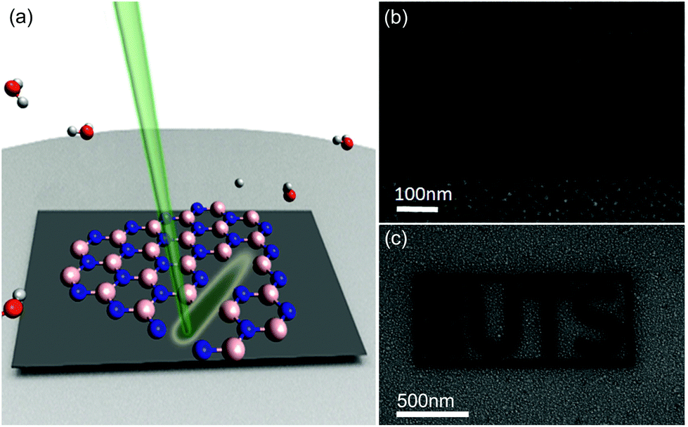 | ||
| Fig. 1 (a) Schematic illustration of electron beam induced etching of hBN performed using H2O vapor as the etch precursor. (b, c) Patterns fabricated in hBN. Dark areas are regions from which hBN was removed by the electron beam. The surface roughness seen in the images is caused by backscattered electrons exiting the sample beyond the region irradiated by the beam. | ||
Bulk hBN grown by a high temperature, high pressure process16 was mechanically exfoliated onto a Si(111) substrate covered with a native oxide layer. The exfoliated hBN flakes on Si were rinsed with acetone and IPA and dried under flowing N2. To perform EBIE,17–22 the hBN samples were mounted onto a heating stage in a customized FEI field emission SEM23 and plasma treated overnight at room temperature with a mild 15 W delocalised plasma in a low vacuum O2 environment of 13 Pa to remove carbon contaminants resulting from the exfoliation process. The plasma treatment improves EBIE repeatability and enables quantitive measurements of etch rates,24 but does not result in etching or damage to the hBN (Fig. S1†). Following plasma cleaning, the system was pumped down to high vacuum and the chamber was filled with water vapor to a pressure of 8 Pa (electron irradiation of hBN in high vacuum gave rise to extremely slow etch rates attributed to the presence of residual H2O in the SEM chamber25). The electron beam current was fixed at 1.35 nA for all EBIE experiments, and the beam energy was either 25 keV (Fig. 3) or 15 keV. Etching was done using a focused, Gaussian electron beam, except for etch pits made to characterize the etch rate as a function of time and temperature (Fig. 5), which were fabricated using a stationary top-hat beam with a diameter of 200 nm. Etch pit depths were measured by atomic force microscopy (AFM). Auger electron analysis was performed ex situ using a nano-Auger Electron Spectrometer (AES, Omicron nanoSAM), in ultrahigh vacuum conditions.
Electron beam irradiation in the presence of H2O vapor gives rise to localized etching of hBN, and the beam can be scanned to create arbitrary, complex patterns deterministically. As examples, we show an array of waveguides in Fig. 1b, and the logo of the University of Technology Sydney in Fig. 1c. The etch technique is very versatile, but gives rise to the surface roughness seen around the etched patterns. To understand and mitigate this roughening, we characterized the time evolution of the etched surface. Initially (i.e., at low electron fluences), the etch process causes roughening of the hBN surface, followed by complete removal of hBN under the electron beam. The time-evolution of the surface morphology is seen in Fig. 2a where regions 1 to 5 correspond to areas of a hBN flake that were irradiated with electron beam fluences of 1.7, 5.1, 11, 19 and 33 × 1020 cm−2, respectively. Fig. 2b shows Auger electron spectra taken from each of the 5 regions shown in Fig. 2a. Regions 1–4 contain boron and nitrogen, and both elements are absent from region 5. The spectra also show that the intensity of the OKLL oxygen peak increases monotonically with electron fluence, and it is most intense in region 5. Thus the increase in oxygen is attributed to the native silicon oxide layer of the substrate. The residual fragments seen in regions 1–4 (Fig. 2a) are comprised of boron and nitrogen, as is illustrated by the high resolution secondary electron image, and the boron, nitrogen and oxygen Auger maps shown in Fig. 2c. Raman spectroscopy was also undertaken before and after EBIE of hBN and shows no change to the hBN Raman line (Fig. S2†).
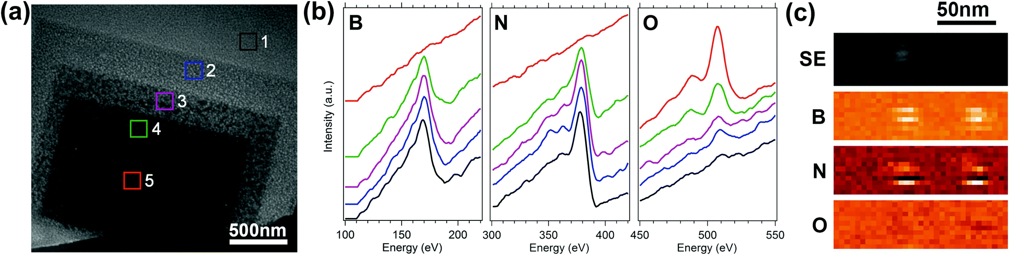 | ||
| Fig. 2 (a) Flake of hBN that was processed using 5 electron doses corresponding to electron beam fluences of 1.7, 5.1, 11, 19 and 33 × 1020 cm−2 (regions 1–5, respectively). (b) Auger electron spectra acquired from the 5 regions shown in a. The peaks correspond to the 170 eV BKLL, 379 eV NKLL and 507 eV OKLL Auger lines. The electron beam energy and current used for Auger analysis were 5 keV 1 nA, respectively. (c) Secondary electron (SE) image and Auger maps of boron nitride fragments generated during etching. | ||
The crystallographic structure of the fragments was confirmed by selected area electron diffraction (SAED). Fig. 3a is a TEM image of a hBN flake that contains a hole (bottom right-hand corner) etched by EBIE. Fig. 3b is a SAED pattern taken from a pristine region of the flake that had not been etched by EBIE, while Fig. 3(c and d) shows patterns from two regions indicated on the TEM image, at the periphery of the etch pit. The material in regions (c) and (d) is residue left behind by incomplete etching. All three diffraction patters were indexed as hBN, confirming that the corresponding contrast seen in SEM images (Fig. 1b, c and 2a) corresponds to hBN fragments. Hence, both the Auger and TEM data show that, during the initial phase of EBIE, low dose electron exposure gives rise to the formation of hBN fragments with a diameter of ∼30 nm, prior to complete volatilization and removal of the boron and nitrogen constituents.
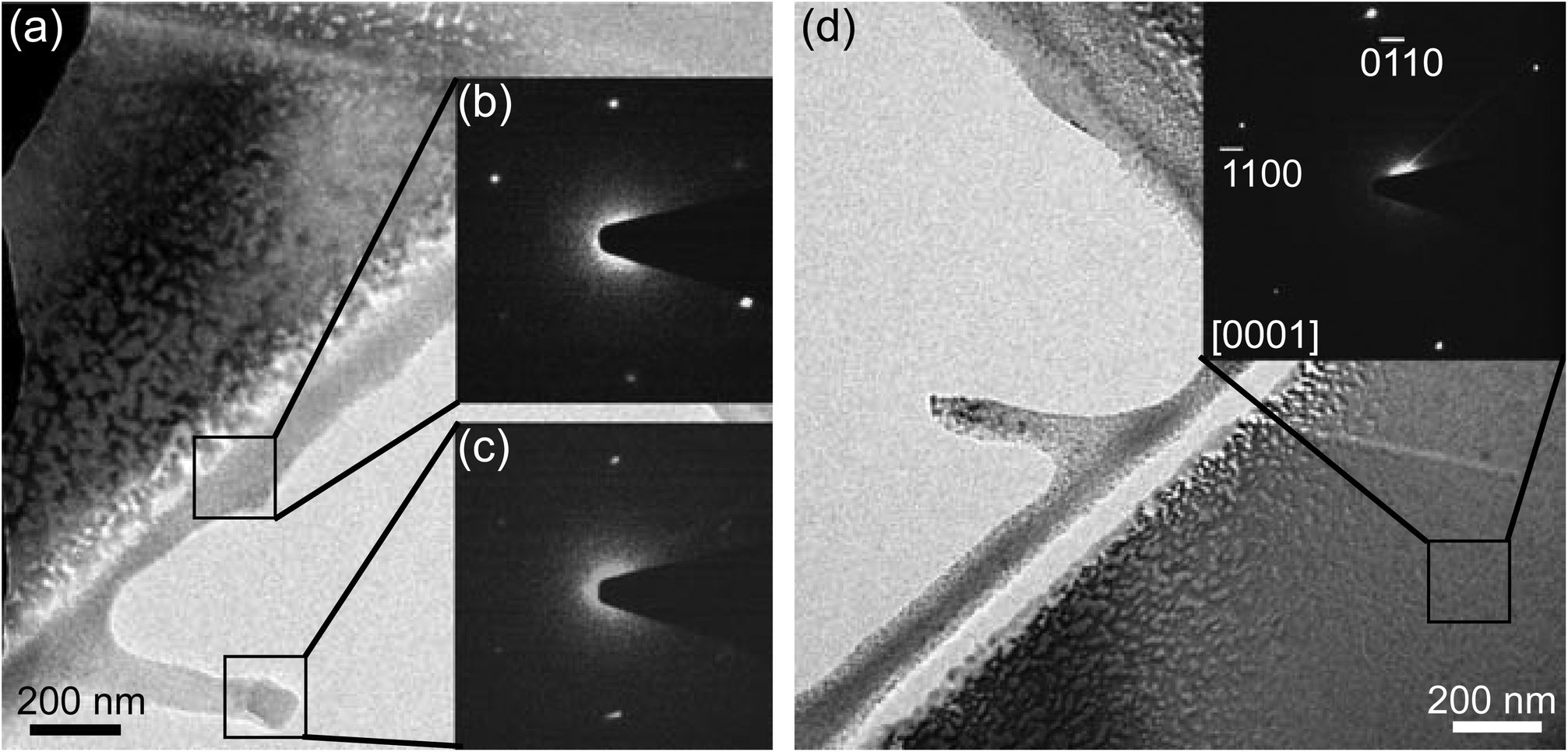 | ||
| Fig. 3 (a) TEM image of a hBN flake that contains an etch pit (bottom right-hand corner) fabricated by EBIE. The insets (b) and (c) show selected area electron diffraction patterns from the regions indicated on the image. The region indicated in (d) shows a pristine area of the hBN flake and the inset shows its corresponding selected area electron diffraction pattern. All patterns were indexed as hBN. | ||
The hBN fragmentation process is problematic for practical applications of the etch technique because it occurs beyond the immediate area irradiated by the electron beam, and hence damages hBN around the patterned nanostructures (see Fig. 1b and c). We attribute this delocalized damage to incomplete etching caused by backscattered electrons (and so-called ‘type II’ secondary electrons26) that are emitted from the sample after a large number of scattering events in the bulk substrate below the hBN. The effect can be suppressed simply by minimizing the size of the electron interaction volume in the sample. This can be achieved either by using a low energy electron beam (e.g. 1 keV whereby the width of the electron interaction volume in most materials is on the order of 10 nm (ref. 27)) or by eliminating the bulk Si substrate. The latter is demonstrated in Fig. 4(a) by a series of lines etched into a hBN flake suspended over a hole in a Si membrane with a 90 nm thermal oxide layer. Fig. 4(b) is a close-up view of the lines, and clearly shows the presence of fragmented hBN around lines that were etched into hBN residing on the Si membrane (left), and absence of such fragments around regions suspended over a hole (right). The reduction in interaction volume over the hole is illustrated in Fig. 4c by electron trajectories simulated for a suspended 100 nm thick flake of hBN (left), and for the same flake residing on a bulk Si substrate (right). The simulations were performed for a 15 keV electron beam using the Monte Carlo package CASINO.28 Further SEM images and Monte Carlo simulations showing the differences in fragmentation and surface roughness of suspended and non-suspended hBN at primary beam energies between 5 and 25 keV are shown in Fig. S3–S5.† These results prove that the delocalized damage is indeed caused by backscattered electrons emitted from the sample, and that it can be suppressed simply by minimizing the size of the electron interaction volume.
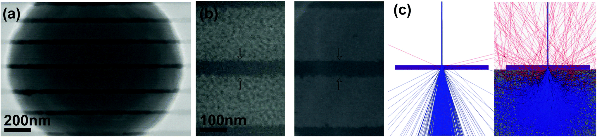 | ||
| Fig. 4 (a) A series of horizontal lines etched into a hBN flake suspended over a 1.3 micron hole in a Si membrane with a 90 nm thermal oxide layer. (b) Close-up image of similar lines (indicated by arrows) showing the presence (left) and absence (right) of surface roughness in hBN residing on top of a bulk substrate and over a hole, respectively. (c) Electron trajectories in a suspended 100 nm multilayer of hBN, and in the same hBN residing on top of a bulk Si substrate. Red lines represent electrons that backscatter out of hBN. The roughness seen in (b) is attributed to backscattered electrons. | ||
Having demonstrated the ability to etch hBN, we now characterize the etch process to gain understanding of the mechanism. Etch rate dependencies on temperature15 and time24 have previously provided key insights into the underlying mechanisms. Hence, Fig. 5 shows plots of etch pit depth versus (a) time and (b) temperature (up to 325 °C), revealing that the etch rate is independent of both parameters. The fact that the etch rate does not increase with time indicates that the electron beam does not create chemically active defects below the top monolayer24 of hBN. The lack of dependence on temperature implies that the H2O precursor molecules dissociate spontaneously, generating chemisorbed species (such as H, O and OH) that bond to the surface and can contribute to etching, irrespective of the substrate temperature15 (up to a temperature of at least 325 °C). The dissociation likely takes place at defects or edges of hBN sheets. Preferential chemisorption at defects may explain the fragmentation of hBN flakes (seen in Fig. 2a) that precedes the complete removal of hBN by EBIE.
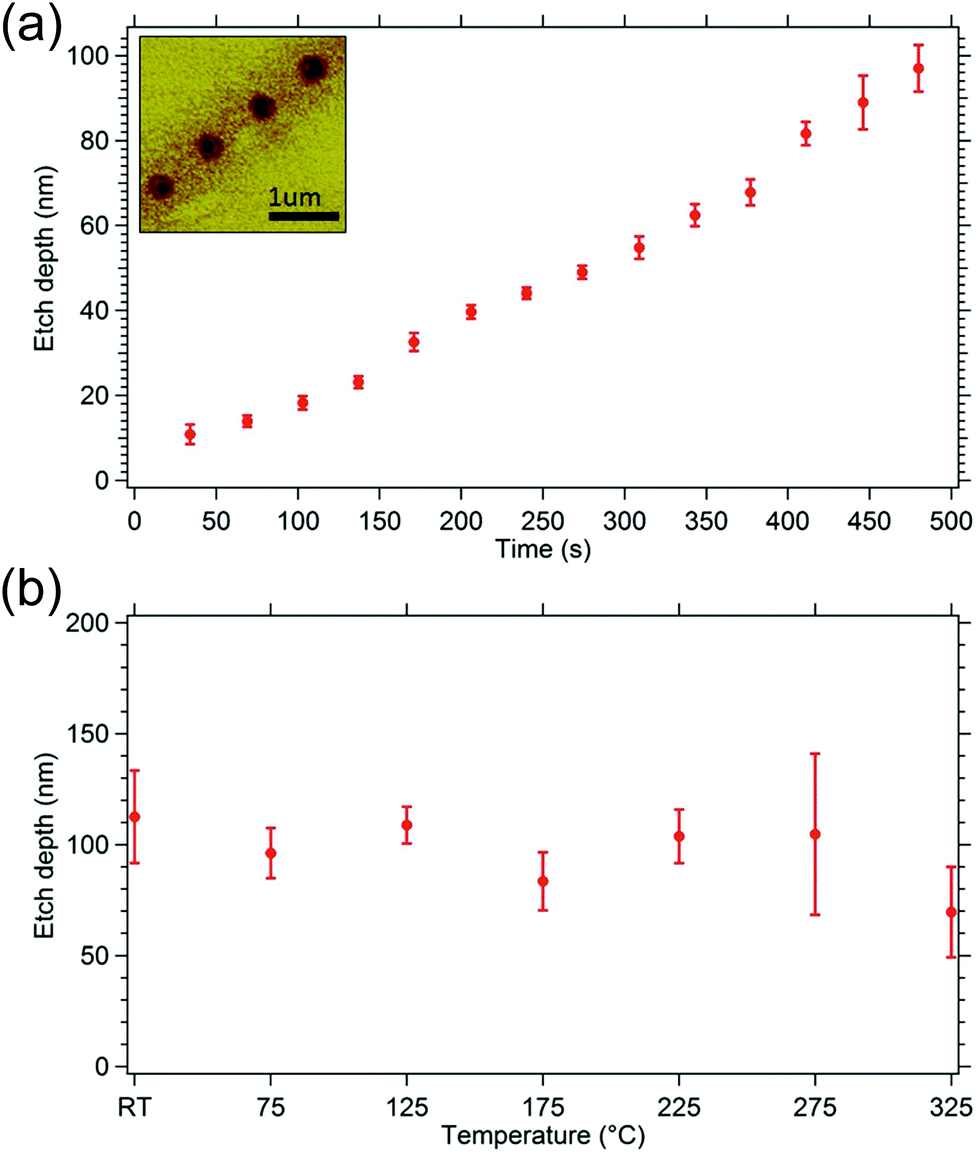 | ||
| Fig. 5 (a) Etch pit depth plotted as a function of etch time at room temperature. The inset is an AFM image of some of the etch pits used to make the plot. (b) Etch pit depth of hBN versus temperature. The electron beam dwell time was 10 minutes at each temperature. | ||
Our current data do not provide direct evidence for the molecular species of the nitrogen and boron-containing reaction products that desorb from the substrate during etching. These molecules are extremely difficult to detect due to the low absolute reaction product generation rates of EBIE. However, we note that the formation of volatile nitrogen-containing molecules is not surprising, as there exist numerous potential candidates such as N2, N2O and NO2. Potential pathways for volatilization of boron are less obvious and may involve the production of borane (BH3) or boric acid (H3BO3).
Finally, we note that the temperature-independence of the etch rate seen in Fig. 5b implies that the critical role of electrons in the etch process is not to dissociate physisorbed precursor molecules (i.e. H2O), as this would result in a rapid, exponential decrease in etch rate with increasing temperature. Instead, a likely key role of the electrons is stimulated desorption of the final reaction products, as has been argued recently for the case of H2O EBIE of single crystal diamond.15
In conclusion, we have demonstrated a novel H2O-mediated electron beam induced etching process that enables high resolution patterning of hBN with nanoscale resolution. The etch process likely proceeds through spontaneous dissociative chemisorption of H2O at defects and at the edges of hBN sheets, fragmentation of hBN into nanoscale hBN fragments, and volatilization of the nitrogen and boron constituents. The etch rate is found to be temperature independent, indicating the role of the electrons is to remove the final reaction products rather than dissociate the H2O precursor molecules. Our results will advance the understanding of hBN chemical stability and accelerate its use in practical optoelectronic and photonic devices.
Acknowledgements
This work was funded by FEI Company and the Australian Research Council. This work is also supported by European Regional Development Fund (CEITEC – CZ.1.05/1.1.00/02.0068) and the Grant Agency of the Czech Republic (Grant No. 15-21581S). M. K. and T. S. acknowledge CF Nano infrastructure for access to the nanoSAM microscope. K. W. and T. T. acknowledge support from the Elemental Strategy Initiative conducted by the MEXT, Japan and a Grant-in-Aid for Scientific Research on Innovative Areas ‘Science of Atomic Layers’ from JSPS.References
- Y. Lin and J. W. Connell, Nanoscale, 2012, 4, 6908–6939 RSC.
- K. Watanabe, T. Taniguchi and H. Kanda, Nat. Mater., 2004, 3, 404–409 CrossRef CAS PubMed.
- J. D. Caldwell, A. V. Kretinin, Y. Chen, V. Giannini, M. M. Fogler, Y. Francescato, C. T. Ellis, J. G. Tischler, C. R. Woods and A. J. Giles, et al., Nat. Commun., 2014, 5, 5221 CrossRef CAS PubMed.
- K. Uosaki, G. Elumalai, H. Noguchi, T. Masuda, A. Lyalin, A. Nakayama and T. Taketsugu, J. Am. Chem. Soc., 2014, 136, 6542–6545 CrossRef CAS PubMed.
- T. T. Tran, K. Bray, M. J. Ford, M. Toth and I. Aharonovich, Nat. Nanotechnol., 2015, 11, 37–41 CrossRef PubMed.
- S. Dai, Z. Fei, Q. Ma, A. Rodin, M. Wagner, A. McLeod, M. Liu, W. Gannett, W. Regan and K. Watanabe, Science, 2014, 343, 1125–1129 CrossRef CAS PubMed.
- L. Wang, B. Wu, L. Jiang, J. Chen, Y. Li, W. Guo, P. Hu and Y. Liu, Adv. Mater., 2015, 27, 4948–4948 CrossRef.
- S. Sharma, G. Kalita, R. Vishwakarma, Z. Zulkifli and M. Tanemura, Sci. Rep., 2015, 5, 10426–10426 CrossRef PubMed.
- Y. Liao, K. Tu, X. Han, L. Hu, J. W. Connell, Z. Chen and Y. Lin, Sci. Rep., 2015, 5, 14510 CrossRef CAS PubMed.
- Z. Liu, L. Ma, G. Shi, W. Zhou, Y. Gong, S. Lei, X. Yang, J. Zhang, J. Yu, K. P. Hackenberg, A. Babakhani, J.-C. Idrobo, R. Vajtai, J. Lou and P. M. Ajayan, Nat. Nanotechnol., 2013, 8, 119–124 CrossRef CAS PubMed.
- J. C. Meyer, A. Chuvilin, G. Algara-Siller, J. Biskupek and U. Kaiser, Nano Lett., 2009, 9, 2683–2689 CrossRef CAS PubMed.
- L. Sun, F. Banhart and J. Warner, MRS Bull., 2015, 40, 29–37 CrossRef CAS.
- G. H. Ryu, H. J. Park, J. Ryou, J. Park, J. Lee, G. Kim, H. S. Shin, C. W. Bielawski, R. S. Ruoff, S. Hong and Z. Lee, Nanoscale, 2015, 7, 10600–10605 RSC.
- S. Linas, R. Fulcrand, F. Cauwet, B. Poinsot and A. Brioude, RSC Adv., 2015, 5, 49231–49234 RSC.
- A. A. Martin, A. Bahm, J. Bishop, I. Aharonovich and M. Toth, Phys. Rev. Lett., 2015, 115, 255501–255501 CrossRef PubMed.
- T. Taniguchi and K. Watanabe, J. Cryst. Growth, 2007, 303, 525–529 CrossRef CAS.
- I. Utke, S. Moshkalev and P. Russell, Nanofabrication using focused ion and electron beams: principles and applications, Oxford University Press, 2012 Search PubMed.
- M. Toth, Appl. Phys. A: Solids Surf., 2014, 117, 1623–1629 CrossRef CAS.
- C. R. Arumainayagam, H.-L. Lee, R. B. Nelson, D. R. Haines and R. P. Gunawardane, Surf. Sci. Rep., 2010, 65, 1–44 CrossRef CAS.
- I. Utke, P. Hoffmann and J. Melngailis, J. Vac. Sci. Technol., B, 2008, 26, 1197–1276 CAS.
- S. J. Randolph, J. D. Fowlkes and P. D. Rack, Crit. Rev. Solid State Mater. Sci., 2006, 31, 55–89 CrossRef CAS.
- I. Utke and A. Goelzhaeuser, Angew. Chem., Int. Ed., 2010, 49, 9328–9330 CrossRef CAS PubMed.
- M. Toth, C. J. Lobo, W. R. Knowles, M. R. Phillips, M. T. Postek and A. E. Vladar, Nano Lett., 2007, 7, 525–530 CrossRef CAS PubMed.
- A. A. Martin, M. R. Phillips and M. Toth, ACS Appl. Mater. Interfaces, 2013, 5, 8002–8007 CAS.
- A. A. Martin, G. McCredie and M. Toth, Appl. Phys. Lett., 2015, 107, 041603 CrossRef.
- J. Goldstein, D. E. Newbury, P. Echlin, D. C. Joy, A. D. Romig Jr., C. E. Lyman, C. Fiori and E. Lifshin, Scanning electron microscopy and X-ray microanalysis: a text for biologists, materials scientists, and geologists, Springer Science & Business Media, 2012 Search PubMed.
- D. Joy and S. Luo, Scanning, 1989, 11, 176–180 CrossRef.
- P. Hovington, D. Drouin and R. Gauvin, Scanning, 1997, 19, 1–14 CrossRef CAS.
Footnote |
| † Electronic supplementary information (ESI) available. See DOI: 10.1039/c6nr04959a |
| This journal is © The Royal Society of Chemistry 2016 |