
 Open Access Article
 This Open Access Article is licensed under a
 Creative Commons Attribution 3.0 Unported Licence
Horizontal carbon nanotube alignment
Matthew T.
Cole
*a,
Vito
Cientanni
a and
William I.
Milne
ab
aDepartment of Engineering, Electrical Engineering Division, University of Cambridge, Cambridge CB3 0FA, UK. E-mail: mtc35@cam.ac.uk
bCollege of Information Sciences & Electronic Engineering, Zhejiang University, Hangzhou, 310027, China
First published on 16th August 2016
Abstract
The production of horizontally aligned carbon nanotubes offers a rapid means of realizing a myriad of self-assembled near-atom-scale technologies – from novel photonic crystals to nanoscale transistors. The ability to reproducibly align anisotropic nanostructures has huge technological value. Here we review the present state-of-the-art in horizontal carbon nanotube alignment. For both in and ex situ approaches, we quantitatively assess the reported linear packing densities alongside the degree of alignment possible for each of these core methodologies.
 Matthew T. Cole | Matthew T. Cole CEng, CPhys, CSci, obtained an MEng in Engineering Sciences from Oxford University, Oxford, UK in 2008 and a PhD in Electrical Engineering from Cambridge University, Cambridge, UK in 2011. He is the Oppenheimer Research Fellow in the Electrical Engineering Division and the Cambridge Graphene Centre, at the Department of Engineering, Cambridge University. Dr Cole's research focuses on the heterogeneous integration of chemical vapor deposited aligned nanomaterials for nanoscale vacuum power electronics devices. He is a Fellow of St Edmunds College, Cambridge where he is Director of Studies in Engineering and Admissions Tutor. He has spent time as a visiting scholar at Harvard University and as a research associate at Sharp Laboratories of Europe. In 2015 Dr Cole was awarded the Institute of Materials, Minerals and Mining's Silver Medal, the Institute of Engineering and Technology's Sir Royce Medal, and the Royal Academy of Engineering's Sir MacFarlane Medal. In 2016 he was named in the inaugural European Forbes 30 under 30 list. |
 Vito Cientanni | Vito Cientanni obtained an MSci in Physics from Imperial College London, UK in 2015. Here he was a member of the Attosecond Laser Science group in the High Energy Physics Department. He has collaborated with the CERN and LUX experiments to develop Dark Matter simulations. He was an exchange student at the University of Science and Technology, Hefei, China with the Plasma Physics Group in the Physics Department, where he built probes to measure plasma spin in a K-MAX linear collider. He is currently a member of the Graphene Technology Center for Doctoral Training, and is currently working on X-ray emission using graphene-based nanosystems. |
 William I. Milne | William I. Milne FREng. FIET, FIMMM obtained a BSc from St Andrews University in Scotland in 1970 and then went on to read for a PhD in Electronic Materials at Imperial College London. He was awarded his PhD and DIC in 1973 and, in 2003, a D.Eng (Honoris Causa) from University of Waterloo, Canada. He was Head of Electrical Engineering, Cambridge University from 1999–2014 and Director of the Centre for Advanced Photonics and Electronics (CAPE) from 2004–2015. In 1996 he was appointed to the “1944 Chair in Electrical Engineering”. His research interests include large area Si and carbon based electronics, graphene, carbon nanotubes and thin film materials. He has published/presented ∼800 papers in these areas, of which 200 were invited. He has an “h” index of 59 (Web of Science). Prof. Milne was elected a Fellow of The Royal Academy of Engineering in 2006. Prof. Milne was awarded the J. J. Thomson medal from the IET in 2008 and the NANOSMAT prize in 2010 for excellence in nanotechnology. |
I. Introduction
Carbon nanotubes (CNTs) have proven potential in a wide range of mechanical, optical and electrical devices whose function is often predicated on the ability to align the nanotubes. Indeed, the capacity to align, en masse, via extremely highly parallelised processes has resulted in the demonstration of a variety of unique devices whose function is dramatically improved relative to their unaligned counterparts. CNT-based optical polarizing media have shown a clear correlation in the magnitude of the polarization selective absorption with the degree of alignment, the typical failure strain in aligned CNT films has been improved by up to an order of magnitude following CNT alignment,1 and thin film transistors based on aligned single-walled CNTs show mobilities up to 40 times higher than randomly orientated devices.2,3 With the continued maturity of carbon nanotube growth and deposition techniques, an extensive variety of horizontal in situ and ex situ alignment techniques have been developed, including, most commonly; roll, scratch, density and field alignment. The ability to rationally synthesis truly self-assembled nanoscale channels, novel optical devices and next generation integrated circuit interconnects has never been closer.CNTs can be aligned (Fig. 1) via; (i) ex situ, also termed post-synthesis, alignment, where external forces such as electric fields (i.e. dielectrophoresis)4,5 orientate the nanotubes once dispersed onto a substrate, often by means of a liquid medium; or via (ii) in situ (aligned synthesis) where the aligning fields are imposed during nanotube growth. Herein we provide a review and comparative meta-analysis of these various alignment techniques.
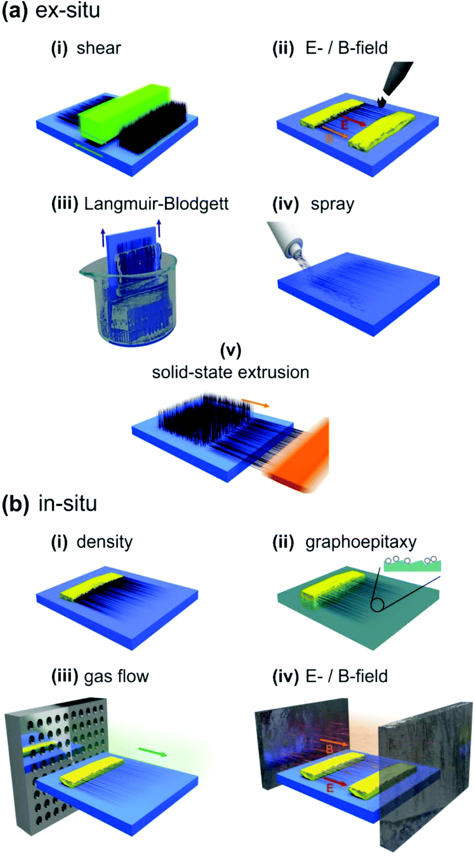 | ||
| Fig. 1 CNT alignment. (a) Ex situ techniques including; (i) mechanical shear, (ii) electric (E) and/or magnetic (B) fields, (iii) Langmuir–Blodgett, (iv) spray coating, and (v) solid-state extrusion. (b) In situ alignment techniques including; (i) packing density, (ii) graphoepitaxy, (iii) gas flow, and (iv) electric (E), magnetic (B) and/or plasma. | ||
II. Ex situ alignment
A number of ex situ, or post-synthesis alignment techniques have been developed to mediate en masse parallel bulk alignment, though these ex situ techniques often experience significant inter-tube interactions which often reduces the degree of alignment. Vertically aligned nanotube forests can be compressed, rolled and sheared;6 though often only approximate directionality is achieved. Such techniques are largely inaccurate and suffer from poor reproducibility. A wide variety of ex situ shearing techniques have been developed; from loading at a predetermined angle, to stretching and compressing vertically aligned CNT forests. These techniques shows some of the highest packing densities recorded (at the thin film surface at least). Bulk assessment remains challenging, though alignment in this technique is dependent on the angle of shear for the pressing technique and is strongly dependent on the user. When compressed from a fixed axis of rotation, varying degrees of misalignment can be introduced, however it has been found that if the press is translated forward as it rotates the alignment can be dramatically improved.Nano-manipulation is another increasingly common method, though the processing is serial and requires time-consuming electron microscopy techniques.7 Spin and drop casting of nanotube suspensions have shown moderate success.8,9 Nevertheless, despite the nanotubes in-plane alignment they have little or no linear directionality, which is to say that there is no controllable way to reproducibly define the mean azimuth, in that the CNTs are merely randomly orientated within the deposition plane. Wei et al.10 demonstrated the use of dielectrophoresis exploiting the weak nanotube dipole. An electric field, of the order of ∼10 V μm−1,11–14 was used to align solution dispersed nanotubes, whereas only ∼1 V μm−1 (ref. 15–17) has been shown to align the nanotubes during synthesis. In contrast, ex situ E-field alignment requires no CNT fixing agent and allows for immediate burning of metallic tubes, should the application call for this. Ex situ E-field approaches often produce varied results, with a degree of alignment commonly less than comparable shear methods. This is likely due to the use of CNT liquid suspensions, with viscous and surface tension largely determining the degree of alignment. The linear packing density associated with this technique was found to be strongly dependent on the ink concentration used.
Ex situ B-field alignment samples are often relatively poorly aligned. Usually suspended within a composite or epoxy, the slowing of the CNTs paramagnetic alignment is critical, as is a fixing agent making the technique impractical for some applications.
Although local electric and magnetic fields have been shown to be promising, the demanding electrode and catalyst patterning processes limits scalability, both in terms of nanotube length and mass production. Practical devices require larger scales. Recently, the fabrication of freestanding alternative, capable of producing significant lengths of free-standing thin films consisting of aligned multi-walled carbon nanotubes without the use of a binder or any supporting substrate has been reported.18 Such structures are often very-well aligned and afford particularly high linear packing densities. There are broadly two types of solid state extrusion that are largely alignment independent; namely those being drawn from vertically aligned CNT forests and those from less orientated aerogels. Little variation in alignment was noted between these.
III. In situ alignment
Density alignment has been achieved by depositing the catalyst material on the vertical face of a sputtered SiO2 protrusion using angled physical vapour deposition. Low-density catalyst particles permit random alignment during growth. This produces classic entangled spaghetti-like networks. In some instances, it is possible to use such thermal randomisation to deposit in-plane nanotubes by careful consideration of the catalyst, diffusion barrier and growth conditions. In-plane alignment is possible, though in-plane directional control is not. Instead, the application of forces during growth can be used to align the nanotubes in plane.Fig. 2 shows SEM micrographs of various reported in situ alignment techniques including; gas flow,22–26 electric field12,15,17 and graphoepitaxy.19–21 Although clear divisions can be discerned between alignment techniques, in practice many groups have exploited (either by happenstance or design) combinations of these in order to optimize the alignment in terms of linear packing density and degree of alignment.
 | ||
| Fig. 2 Examples of in situ CNT alignment via; (a) gas flow,42,43 (b) electric field,13,16 and (c) graphoepitaxy.44 | ||
Nanotubes graphoepitaxially align to surface nanofacets during growth. The technique is surface morphology sensitive which limits the broadness of the technique. Nevertheless, recently impressive rudimentary computational devices based on these aligned horizontal architectures have been realised.27 High degrees of alignment and uniformity have been evidenced through the production of highly linear, regular and periodic arrays.21,28 Despite this, the process involves time-consuming surface preparatory processes and requires expensive substrates, such as sapphire or quartz. Rational substrate design, using elevated Si pillars, offers an alternative approach.29 Here the nanotubes grow between elevated pillars. The micrometer pillars limit the practicality of the technique as well as restricting the maximum packing density. As a result, techniques based on electric field and gas flow alignment show perhaps the most promise. They are rapid, parallel processes that offer simplicity and the ability to fabricate high density arrays.
During CVD-synthesis it is also possible to align using the growth gases. Here the growth and carrier gases flow parallel to the catalyst-carrying substrate and it is this which induces the alignment during the growth. Huang,25 Xin,26 and Jin et al.![[thin space (1/6-em)]](https://www.rsc.org/images/entities/char_2009.gif) 24 have all demonstrated gas flow alignment with varying degrees of success. Xin et al.26 showed, in a gas flow cell, free stream velocities of up to 9 cm s−1 were necessary for aligned growth, though the SiO2 surfaces nonetheless ultimately passivated the growth irrespective of the flow rate. The gas flow can both enhance and degrade the degree of alignment; turbulent flow has been seen to degrade the alignment in otherwise high-packing density well-aligned samples. The magnitude of the forces relating to the turbulent flow may very well dominate those associated with the underlying catalysis, ∼0.5 μN for nominal 45° misalignment.16 The flow regime must therefore be critically considered via a growth chamber specific Reynolds number, which is principally dictated by the characteristic dimension of the flow-perturbing feature within the growth chamber, as well as the free-stream flow velocity and the kinematic viscosity of the growth gaseous species. Based on Sun et al.,30 at 700 °C and for a predominately NH3 flow at 5 mbar, where the etchant gas has a much higher flow rate than the carbon precursor, for most cold-walled reactors with a central heating stage of the order of 5 cm in size, a predominately laminar flow is certainly viable. Nevertheless, few have pursued this avenue in practice, likely in part associated with the challenging issue of micro-eddy formation which places strict upper limits on the degree of alignment.
24 have all demonstrated gas flow alignment with varying degrees of success. Xin et al.26 showed, in a gas flow cell, free stream velocities of up to 9 cm s−1 were necessary for aligned growth, though the SiO2 surfaces nonetheless ultimately passivated the growth irrespective of the flow rate. The gas flow can both enhance and degrade the degree of alignment; turbulent flow has been seen to degrade the alignment in otherwise high-packing density well-aligned samples. The magnitude of the forces relating to the turbulent flow may very well dominate those associated with the underlying catalysis, ∼0.5 μN for nominal 45° misalignment.16 The flow regime must therefore be critically considered via a growth chamber specific Reynolds number, which is principally dictated by the characteristic dimension of the flow-perturbing feature within the growth chamber, as well as the free-stream flow velocity and the kinematic viscosity of the growth gaseous species. Based on Sun et al.,30 at 700 °C and for a predominately NH3 flow at 5 mbar, where the etchant gas has a much higher flow rate than the carbon precursor, for most cold-walled reactors with a central heating stage of the order of 5 cm in size, a predominately laminar flow is certainly viable. Nevertheless, few have pursued this avenue in practice, likely in part associated with the challenging issue of micro-eddy formation which places strict upper limits on the degree of alignment.
Law et al.12 found, for electric field alignment, that plasma induced self-biasing and the resultant surface charging effects on metallic electrodes were sufficient to align the nanotubes, whereas Zhang et al.16 and Ural et al.15 reported similar alignment effects ascribed to globally applied electric fields of the order of 0.5–4.0 V μm−1. They argued that the nanotubes highly anisotropic polarisability induces large dipole moments when they interact with the local electric field. This interaction produces large aligning torques which governs the resulting growth orientation. Blaek et al.31 estimated the electric field aligning force to be of the order of 10−5 nN, a force approximately four orders of magnitude greater than the weight of the catalyst particle. Hertel et al.32 estimated that a 10 nm wide nanotube experiences a per unit length van der Waals surface binding force of the order of 35 nN, supporting the observed nanotube substrate mediated growth termination in many density alignment experiments.
Few comprehensive attempts have been made to explain the orientation mechanisms involved; challenges arise in decoupling the evident catalysis with the alignment processes. Indeed, it may be such that the two cannot be decoupled faithfully. Nevertheless, low gas flow rates (<2 cm s−1) are often used to avoid turbulent interactions. Chen et al.33 proposed a so-called kite growth mechanism. Here the catalyst particle, located, in this instance at the nanotube apex, was forced in the direction of the prevailing electric field (or gas flow) at a largely uncontrolled, and time varying, angle from the substrate. When the growth terminates the nanotubes fell to the substrate, where they subsequently become strongly bound. Huang et al.22 presented a similar mechanism, whereas Yu et al.34 postulated that charged species form bonds along the electric field direction and that the nanotubes can only grow if they align to the electric field. Tanemura et al.35 suggested that the alignment effect may be a result of an excess of electrostatically attracted positive charge ions at the nanotube tips. They concluded that the ions, radicals and excited molecular species in the incident plasma play a decisive role in the alignment by reducing the lateral mechanical stress exerted on the nanotubes. The combined findings of ref. 15, 16, 36 and 37 indicate that an electric field in the range of 0.1–2.0 V μm−1 is necessary for in situ electric field alignment. Jang et al.17 reported negligible improvements in the alignment ‘quality’ for fields >2.0 V μm−1, whilst Ural et al.15 found an optimal field of 0.1 V μm−1.
Other than the low-linear densities, a significant limitation to local electric-field alignment is the requirement for micro and macro electrodes, patterned directly on the planar substrate; this certainly limits the approach to those technologies that have few metallic features on the substrate to be coated, such as anisotropic optical media. Such structures interfere greatly with post-growth processing and device fabrication. Substrate independent electrodes obviate the limitations of the patterned electrode. The electric field can then be applied across the entire sample. Such an approach has been widely demonstrated in a vertical context; however, to the best of the author's knowledge, no one has hitherto demonstrated such alignment convincingly in plane.
It has been widely postulated that, as for vertical nanotube growth, alignment is achieved by anisotropic torque induction within a narrow plasma sheath.38 This sheath exists in the narrow glow region, ∼3 mm wide, adjacent to the biased cathode. In the case of a horizontal CNT plasma enhanced chemical vapour deposition system, for typical process conditions, in a Child's Law like plasma in a quasi-neutral Maxwellian regime, the local charge carrier density ne = 2.5 × 10¹⁷ m−3 and the local electron temperature, Te = 0.7 eV; values which show excellent agreement with those reported by Blaek et al.31 The electron density linearly increases with plasma power39 and quadratically decays with pressure. The electron temperature is independent of plasma power and exponentially decays with increasing reactor pressure. Sheath elongation, and hence an increase in the alignment length is therefore possible by decreasing the plasma power, where it is also worth noting that the electron density and temperature decrease with increasing reactor pressure.39,40
Fig. 3 shows the variation in the qualitative degree of alignment as assessed via the Herman's orientation factor (f) as a function of the linear packing density (LPD) for various ex situ and in situ techniques. If not stated in the manuscript directly, the LPD was quantitatively determined via grey-scale image analysis using ImageJ. To calculate the Herman's orientation factor we first process the Fast Fourier Transform (FFT) on the square-cropped collective SEM imagery. From the resulting power spectrum, we extract the azimuthal average to obtain the intensity (I)–azimuthal angle (δ) distribution, which is subsequently used to calculate the Herman's orientation factor (f), as given by:
 | (1) |
 | (2) |
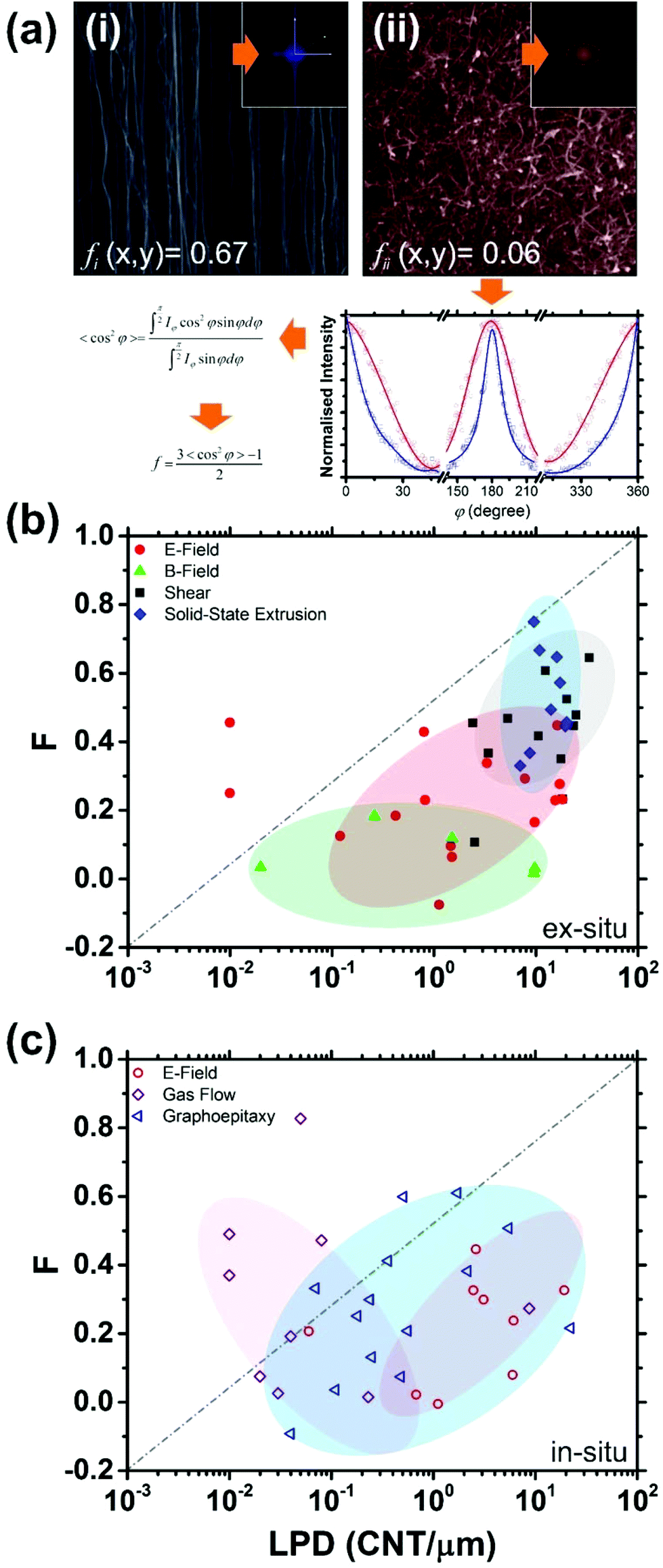 | ||
| Fig. 3 (a) Degree of alignment quantification. Example scanning electron micrographs of (i) well-aligned45 and (ii) largely misaligned46 films with (inset) associated FFT generation and Herman's orientation factor (f) fitting. Herman's orientation factor as a function of Linear Packing Density (LPD) for various published horizontal alignment techniques; (b) ex situ (E-field,46–67 B-field,68–76 shear,1,77–87 and solid-state extrusion45,88–100) and (c) in situ (E-field,101–108 flow directed,109–117 and graphoepitaxy118–135). | ||
The f-factor takes values in the range of −0.5 ≤ f ≤ 1.0. For f = 1.0 the nanotubes are perfectly aligned to the azimuth, f = 0 denotes a random orientation, and f = −0.5 for alignment perpendicular to the azimuth. No images produced f < 0 as, in all cases, for ensured compatibility, all images were aligned with their primary axis parallel to the azimuth prior to the assessment. All processing was conducted using Origin Pro 8.
Though set-to-set comparison is challenging, variations of f within individual production techniques is somewhat revealing. Though coarse assignment is possible, we stress that intentional and unintentional combinations of alignment processes have been developed and unavoidably included herein, making it challenging to demarcate well-defined zones, as does some non-commensurate real-space length scale variations within images. Nevertheless, we stress here that the aim of Fig. 3(b) and (c) is not to draw strict relationships between f and the LPD. Indeed, for some techniques there appears little correlation; a testament to the alignment techniques robustness towards variation as a function of LPD. Despite this, and though somewhat noisy, there does appear to be, in the case of the ex situ techniques, a modest positive correlation between f and LPD; the higher the LPD the greater the f, suggesting that packing effects play at least some role in enhancing alignment in most of the alignment techniques. Such a correlation is yet to be clearly identified in the case of ex situ B-field alignment, likely due to a lack of source data. It is evident that shear alignment, and other mechanical approaches such as solid-state extrusion, proffer the highest LPD, with correspondingly high f (∼ 0.7), making them well-suited for the formation of mechanically anisotropic components, though in situ techniques exploiting lattice faceting, such as graphoepitaxy via thermally derived and artificially patterned facets, are clearly making significant headway towards high alignment (f ∼ 0.6), though with typical LPDs at least an order of magnitude less that ex situ shearing. Both in situ and ex situ E-field alignment appear deficient in terms of alignment, with LPDs ranging from 10−2–101 CNT per μm. There appears a similarity in the approximate f-LPD space for ex situ E- and B-field techniques, with the f of both likely strongly influenced by other factors local to the deposition, such as Brownian motion within the carrier solution. Indeed, we also note similar f-LPD zoning for both in situ and ex situ E-field alignment, largely testifying to the reduced robustness of the approach towards local environmental variations, which, in the case of in situ CVD approaches are a product of local and transient turbulence in the growth gases and potentially significant thermal spatial and temporal variations. Further variation in the LPD distribution for in situ gas aligned samples is largely attributed to the predetermined catalyst loading and the resultant heterogeneous catalysis therein. Nonetheless, both ex situ E- and B-field techniques fail to compete with in situ graphoepitaxy, ex situ shearing and ex situ solid-state extrusion. Solid-state extrusion, though having perhaps the highest mean f, some 10% or so more than shearing, is particularly competitive, especially given its substrate independent formation. Indeed, solid-state extrusion also appears, at present, to be one of the most reproducible techniques, showing some of the lowest variation in LPD of all the techniques considered (6–50 CNTs per μm). Given the high cost of suitable graphoepitaxy substrates and the time consuming thermal pre-processing required to derive suitable lattice facets, shearing and solid-state extrusion approaches appear the most commercially attractive approaches to date, with some of the highest yields and lowest costs. Nevertheless, the need for high packing density and vertical CNT synthesis, which is becoming increasingly common place and is readily achieved by many using simple low-cost growth reactors, is critical, as is improved reproducibility in the alignment processes, without which such approaches will fail to gain industrial traction.
IV. Outstanding challenges
Not all applications require high LPD. In situ approaches are evidently well-suited for such technological needs. However, there are, at the time of publication, very few dedicated commercial growth reactors designed specifically to mediate horizontal CNT growth and certainly none that allow for synthesis at industrially viable scales, albeit at high LPD or otherwise. There is a dramatic gap in the commercial space. Much progress has nonetheless been made in the attaining high f with correspondingly high LPDs, making the use of carbon nanotubes in advanced electronics and optics more viable than ever before.Though horizontal alignment has been demonstrated by many this has almost exclusively been focused on alignment across entire arrays. To date very little has been reported on the development of ad hoc, adjustable in-plane CNT alignment, either in situ or ex situ. Indeed, the ability to controllably align the in-plane angle of CNTs, across entire arrays, or more localized directional control within an array, will open up a huge variety of technologies that have hitherto required the use of high-resolution lithographic processing as well as multiple nanotube transfers based on often complex and cumbersome processes. Though some reports have evidenced bi-directional serpentine-like in-plane growth,41 as a result of spontaneous and largely uncontrolled facet alignment, the ability to accurately control the alignment direction remains a particularly difficult research topic to broach.
As required by many applications, the desirably high catalyst density, and hence nanotube linear density results in zones of misalignment due to strong randomising inter-nanotube interactions. Reductions in catalyst density would certainly be favorable, though potentially at the expense of final device functionality. For example, such a methodology may produce CNT–FETs with superiorly aligned channel regions, though at the cost of fewer transport routes within the channel. Nevertheless, to fully exploit aligned nanotubes in many applications, it is certainly evident that significantly longer nanotubes are necessary, as is concurrent high alignment necessitating the development of various time-consuming repeat-growths or repeat transfer (most likely polymer-mediated), as recently reported.27 The effects of such repeat transferring on the underlying transport remain largely unclear, though the effects seem somewhat functionally marginal.
In the present study we have focused exclusively on the horizontal alignment of CNTs. In the case of the in situ techniques it is important to note that though there is a significant interplay between the growth conditions and the degree of alignment, there too exists an interaction between the growth processes and the nanotube length, chirality, and type, along with other critical physical and technological characteristics. All are central design parameters and must be considered independently and with care in order to realise particular functional systems.
Though the processing challenges remain wide, various further commercial challenges remain. Many such issues that plague the adoption of some of the techniques reported above are common to those plaguing the broader family of emerging carbon nanotube-based technologies. The initially high cost per unit mass has reduced substantially. CNTs are now routinely synthesised at costs of <$10 per g. Though beneficial, such cost reductions are only important for those applications requiring significant volumes of aligned CNTs. In practice, most applications which require high degrees of alignment do not often fall into this category. Indeed, for many, if not all, electronic and interconnect applications, the cost per unit mass determines little the technologies appeal. Rather the adoption reticence of the wider foundry communities has proven a particularly challenging obstacle to navigate. Nevertheless, just as novel nano- and micro-scale devices based on horizontally aligned CNTs are being rapidly reported, many new markets and commercial entities, floated by larger research embracing conglomerates, are appearing at rate, with these aligned horizontal CNT technologies achieving ever higher technology readiness levels. Yield, single-chirality and reproducibility endure as common barriers to scale-up, as does the need for ever higher packing densities, especially if such nanoscale systems are to compete with current metallic interconnects in integrated circuits. Nonetheless the field continues to gain traction.
V. Conclusions
Though significant progress has been made these past two decades, the varied challenges associated with horizontal alignment of carbon nanotubes persist. Both the commercial and fundamental research barriers to wider scale adoption are significant. Nevertheless, with continued maturity many of the outlined techniques are proving ever more fruitful, with ex situ shearing and solid-state extrusion approaches achieving concurrently high packing densities and high alignment, gaining them attention, particularly for en masse production. In contrast, in situ graphoepitaxy currently dominates the fore, with the bottom-up synthesis of nanostructured periodic arrays having much appeal for the realization of nanotube-based computers. Whether carbon nanotubes will achieve future commercial success is unclear, though with further optimization alongside the on-going dominance of the one-dimensional nanostructures and the wider family of nanotechnologies, there remains optimism that one, if not many, of the techniques discussed herein will be employed commercially, at least in one guise or another.Acknowledgements
The authors thank Dr Guofang Zhong, Cambridge University, for assistance in f-factor computation. MTC thanks the Isaac Newton Trust and Oppenheimer Trust, Cambridge University for generous financial support. VC thanks the EPSRC Graphene Doctoral Training Centre. This work was supported by an Impact Acceleration grant from the Engineering and Physical Sciences Research Council and a Royal Society International Exchange grant.References
- W. Xu, Y. Chen, H. Zhan and J. N. Wang, Nano Lett., 2016, 16, 946–952 CrossRef CAS PubMed.
- Q. Cao, S. H. Hur, Z. T. Zhu, Y. G. Sun, C. J. Wang, M. A. Meitl, M. Shim and J. A. Rogers, Adv. Mater., 2006, 18, 304–309 CrossRef CAS.
- F. N. Ishikawa, H.-K. Chang, K. Ryu, P.-C. Chen, A. Badmaev, L. G. De Arco, G. Shen and C. Zhou, ACS Nano, 2009, 3, 73–79 CrossRef CAS PubMed.
- P. A. Smith, C. D. Nordquist, T. N. Jackson, T. S. Mayer, B. R. Martin, J. Mbindyo and T. E. Mallouk, Appl. Phys. Lett., 2000, 77, 1399–1401 CrossRef CAS.
- K. Yamamoto, S. Akita and Y. Nakayama, J. Phys. D: Appl. Phys., 1998, 31, 34–36 CrossRef.
- M. T. Cole, PhD, University of Cambridge, 2011.
- N. De Jonge, M. Allioux, M. Doytcheva, M. Kaiser, K. B. K. Teo, R. G. Lacerda and W. I. Milne, Appl. Phys. Lett., 2004, 85, 1607–1609 CrossRef CAS.
- D. S. Hecht and G. Gruner, Solution Cast Films of Carbon Nanotubes for Transparent Conductors and Thin Film Transistors, Springer Science+Business Media LLC, New York, USA, 2009 Search PubMed.
- H. Ago, K. Petritsch, M. S. P. Shaffer, A. H. Windle and R. H. Friend, Adv. Mater., 1999, 11, 1281–1285 CrossRef CAS.
- Y. Wei, C. Xie, K. A. Dean and B. F. Coll, Appl. Phys. Lett., 2001, 79, 4527–4529 CrossRef CAS.
- P. Kim and C. M. Lieber, Science, 1999, 286, 2148–2150 CrossRef CAS PubMed.
- J. B. K. Law, C. K. Koo and J. T. L. Thong, Appl. Phys. Lett., 2007, 91, 2431081–2431083 Search PubMed.
- E. Joselevich and C. M. Lieber, Nano Lett., 2002, 2, 1137–1141 CrossRef CAS.
- M. Maeda, C. K. Hyon, T. Kamimura, A. Kojima, K. Sakamoto and K. Matsumoto, Jpn. J. Appl. Phys., 2005, 44, 1585–1587 CrossRef CAS.
- A. Ural, Y. M. Li and H. J. Dai, Appl. Phys. Lett., 2002, 81, 3464–3466 CrossRef CAS.
- Y. Zhang, A. Chang, J. Cao, Q. Wang, W. Kim, Y. Li, N. Morris, E. Yenilmez, J. Kong and H. Dai, Appl. Phys. Lett., 2001, 79, 3155–3157 CrossRef CAS.
- Y. T. Jang, J. H. Ahn, B. K. Ju and Y. H. Lee, Solid State Commun., 2003, 126, 305–308 CrossRef CAS.
- M. T. Cole, M. Doherty, R. Parmee, P. Dawson and W. I. Milne, Adv. Opt. Mater., 2014, 2(10), 929–937 CrossRef CAS.
- N. Ishigami, H. Ago, T. Nishi, K. I. Ikeda, M. Tsuji, T. Ikuta and K. Takahashi, J. Am. Chem. Soc., 2008, 130, 17264–17265 CrossRef CAS PubMed.
- L. Ding, D. N. Yuan and J. Liu, J. Am. Chem. Soc., 2008, 130, 5428–5429 CrossRef CAS PubMed.
- A. Ismach, D. Kantorovich and E. Joselevich, J. Am. Chem. Soc., 2005, 127, 11554–11555 CrossRef CAS PubMed.
- L. M. Huang, X. D. Cui, B. White and S. P. O'Brien, J. Phys. Chem. B, 2004, 108, 16451–16456 CrossRef CAS.
- X. Huijun and A. T. Woolley, Nano Lett., 2004, 4, 1481–1484 CrossRef.
- Z. Jin, H. Chu, J. Wang, J. Hong, W. Tan and Y. Li, Nano Lett., 2007, 7, 2073–2079 CrossRef CAS PubMed.
- S. Huang, X. Cai and J. Liu, J. Am. Chem. Soc., 2003, 125, 5636–5637 CrossRef CAS PubMed.
- H. Xin and A. T. Woolley, Nano Lett., 2004, 4, 1481–1484 CrossRef CAS.
- M. M. Shulaker, G. Hills, N. Patil, H. Wei, H.-Y. Chen, H. S. P. Wong and S. Mitra, Nature, 2013, 501, 526–530 CrossRef CAS PubMed.
- A. Ismach and E. Joselevich, Nano Lett., 2006, 6, 1706–1710 CrossRef CAS PubMed.
- A. M. Cassell, N. R. Franklin, T. W. Tombler, E. M. Chan, J. Han and H. J. Dai, J. Am. Chem. Soc., 1999, 121, 7975–7976 CrossRef CAS.
- S. B. K. Sun and T. S. Storvick, J. Chem. Eng. Data, 1979, 24, 88–91 CrossRef CAS.
- J. Blaek, P. Špatenka, F. Pácal, Ch. Täschner and A. Leonhardt, Thin Solid Films, 2005, 489, 291–295 CrossRef CAS.
- T. Hertel, R. E. Walkup and P. Avouris, Phys. Rev. B: Condens. Matter Mater. Phys., 1998, 58, 13870–13873 CrossRef CAS.
- Y. Chen, L. Guo, S. Patel and D. T. Shaw, J. Mater. Sci., 2000, 35, 5517–5521 CrossRef CAS.
- J. Yu, X. D. Bai, J. Ahn, S. F. Yoon and E. G. Wang, Chem. Phys. Lett., 2000, 323, 529–533 CrossRef CAS.
- M. Tanemura, K. Iwata, K. Takahashi, Y. Fujimoto, F. Okuyama, H. Sugie and V. Filip, J. Appl. Phys., 2001, 90, 1529–1533 CrossRef CAS.
- C. Bower, W. Zhu, S. H. Jin and O. Zhou, Appl. Phys. Lett., 2000, 77, 830–832 CrossRef CAS.
- T. Matsuda, M. Mesko, T. Ishikawa, J. Sato, A. Ogino, R. Tamura and M. Nagatsu, Jpn. J. Appl. Phys., 2008, 47, 7436–7439 CrossRef CAS.
- M. Chhowalla, K. B. K. Teo, C. Ducati, N. L. Rupesinghe, G. A. J. Amaratunga, A. C. Ferrari, D. Roy, J. Robertson and W. I. Milne, J. Appl. Phys., 2001, 90, 5308–5317 CrossRef CAS.
- T. M. Desai, S. V. Gogawale, A. B. Shukla, N. K. Joshi, U. S. Salgaonkar and G. L. Bhale, Vacuum, 1995, 46, 223–226 CrossRef CAS.
- M. S. Shah, M. Salem, R. Ahmad, M. Zakaullah, A. Qayyum and G. Murtaza, J. Mater. Process. Technol., 2008, 199, 363–368 CrossRef CAS.
- Y. Ma, B. Wang, Y. Wu, Y. Huang and Y. Chen, Carbon, 2011, 49, 4098–4110 CrossRef CAS.
- S. M. Huang, B. Maynor, X. Y. Cai and J. Liu, Adv. Mater., 2003, 15, 1651–1655 CrossRef CAS.
- Z. Jin, H. B. Chu, J. Y. Wang, J. X. Hong, W. C. Tan and Y. Li, Nano Lett., 2007, 7, 2073–2079 CrossRef CAS PubMed.
- C. Kocabas, S. H. Hur, A. Gaur, M. A. Meitl, M. Shim and J. A. Rogers, Small, 2005, 1, 1110–1116 CrossRef CAS PubMed.
- L. Xiao, Z. Chen, C. Feng, L. Liu, Z.-Q. Bai, Y. Wang, L. Qian, Y. Zhang, Q. Li, K. Jiang and S. Fan, Nano Lett., 2008, 8, 4539–4545 CrossRef CAS PubMed.
- K. Bubke, H. Gnewuch, M. Hempstead, J. Hammer and M. L. H. Green, Appl. Phys. Lett., 1997, 71, 1906–1908 CrossRef CAS.
- M. Arguin, F. Sirois and D. Therriault, Adv. Manuf.: Polym. Compos. Sci., 2015, 1, 16–25 Search PubMed.
- S. Banerjee, B. E. White, L. Huang, B. J. Rego, S. O'Brien and I. P. Herman, J. Vac. Sci. Technol., B, 2006, 24, 3173–3178 CAS.
- A. R. Boccaccini, J. Cho, J. A. Roether, B. J. C. Thomas, E. Jane Minay and M. S. P. Shaffer, Carbon, 2006, 44, 3149–3160 CrossRef CAS.
- X. Q. Chen, T. Saito, H. Yamada and K. Matsushige, Appl. Phys. Lett., 2001, 78, 3714–3716 CrossRef CAS.
- J. Chung, K.-H. Lee, J. Lee and R. S. Ruoff, Langmuir, 2004, 20, 3011–3017 CrossRef CAS PubMed.
- S. M. Jung, H. Y. Jung and J. S. Suh, Carbon, 2007, 45, 2917–2921 CrossRef CAS.
- S. M. Jung, H. Y. Jung and J. S. Suh, Carbon, 2008, 46, 1973–1977 CrossRef CAS.
- P. V. Kamat, K. G. Thomas, S. Barazzouk, G. Girishkumar, K. Vinodgopal and D. Meisel, J. Am. Chem. Soc., 2004, 126, 10757–10762 CrossRef CAS PubMed.
- P. Li and W. Xue, Nanoscale Res. Lett., 2010, 5, 1072–1078 CrossRef CAS PubMed.
- X. Liu, J. L. Spencer, A. B. Kaiser and W. M. Arnold, Curr. Appl. Phys., 2004, 4, 125–128 CrossRef.
- C. A. Martin, J. K. W. Sandler, A. H. Windle, M.-K. Schwarz, W. Bauhofer, K. Schulte and M. S. P. Shaffer, Polymer, 2005, 46, 877–886 CrossRef CAS.
- A. K. Murugesh, A. Uthayanan and C. Lekakou, Appl. Phys. A: Mater. Sci. Process., 2010, 100(1), 135–144 CrossRef CAS.
- C. Park, J. Wilkinson, S. Banda, Z. Ounaies, K. E. Wise, G. Sauti, P. T. Lillehei and J. S. Harrison, J. Polym. Sci., Part B: Polym. Phys., 2006, 44, 1751–1762 CrossRef CAS.
- B. K. Sarker, M. R. Islam, F. Alzubi and S. I. Khondaker, Mater. Express, 2011, 1, 80–85 CrossRef CAS.
- M. Senthil Kumar, T. H. Kim, S. H. Lee, S. M. Song, J. W. Yang, K. S. Nahm and E.-K. Suh, Chem. Phys. Lett., 2004, 383, 235–239 CrossRef.
- M. Senthil Kumar, S. H. Lee, T. Y. Kim, T. H. Kim, S. M. Song, J. W. Yang, K. S. Nahm and E.-K. Suh, Solid-State Electron., 2003, 47, 2075–2080 CrossRef CAS.
- H.-W. Seo, C.-S. Han, D.-G. Choi, K.-S. Kim and Y.-H. Lee, Microelectron. Eng., 2005, 81, 83–89 CrossRef CAS.
- S. Shekhar, P. Stokes and S. I. Khondaker, ACS Nano, 2011, 5, 1739–1746 CrossRef CAS PubMed.
- M.-W. Wang, T.-C. Hsu and C.-H. Weng, Eur. Phys. J.: Appl. Phys., 2008, 42, 241–246 CrossRef CAS.
- K. Yamamoto, S. Akita and Y. Nakayama, Jpn. J. Appl. Phys., 1996, 35, L917 CAS.
- Y.-F. Zhu, C. Ma, W. Zhang, R.-P. Zhang, N. Koratkar and J. Liang, J. Appl. Phys., 2009, 105, 054319 CrossRef.
- E. Camponeschi, R. Vance, M. Al-Haik, H. Garmestani and R. Tannenbaum, Carbon, 2007, 45, 2037–2046 CrossRef CAS.
- E. S. Choi, J. S. Brooks, D. L. Eaton, M. S. Al-Haik, M. Y. Hussaini, H. Garmestani, D. Li and K. Dahmen, J. Appl. Phys., 2003, 94, 6034–6039 CrossRef CAS.
- M. A. Correa-Duarte, M. Grzelczak, V. Salgueiriño-Maceira, M. Giersig, L. M. Liz-Marzán, M. Farle, K. Sierazdki and R. Diaz, J. Phys. Chem. B, 2005, 109, 19060–19063 CrossRef CAS PubMed.
- B. K. Jang, Y. Sakka and S. K. Woo, J. Phys.: Conf. Ser., 2009, 156, 012005 CrossRef.
- T. Kimura, H. Ago, M. Tobita, S. Ohshima, M. Kyotani and M. Yumura, Adv. Mater., 2002, 14, 1380–1383 CrossRef CAS.
- G. Piao, F. Kimura, T. Takahashi, Y. Moritani, H. Awano, S. Nimori, K. Tsuda, K. Yonetake and T. Kimura, Polym. J., 2007, 39, 589–592 CrossRef CAS.
- J. Shaver, A. N. G. Parra-Vasquez, S. Hansel, O. Portugall, C. H. Mielke, M. von Ortenberg, R. H. Hauge, M. Pasquali and J. Kono, ACS Nano, 2009, 3, 131–138 CrossRef CAS PubMed.
- B. W. Steinert and D. R. Dean, Polymer, 2009, 50, 898–904 CrossRef CAS.
- D. A. Walters, M. J. Casavant, X. C. Qin, C. B. Huffman, P. J. Boul, L. M. Ericson, E. H. Haroz, M. J. O'Connell, K. Smith, D. T. Colbert and R. E. Smalley, Chem. Phys. Lett., 2001, 338, 14–20 CrossRef CAS.
- P. D. Bradford, X. Wang, H. Zhao, J.-P. Maria, Q. Jia and Y. T. Zhu, Compos. Sci. Technol., 2010, 70, 1980–1985 CrossRef CAS.
- J. Di, X. Wang, Y. Xing, Y. Zhang, X. Zhang, W. Lu, Q. Li and Y. T. Zhu, Small, 2014, 10, 4606–4625 CrossRef CAS PubMed.
- X. N. He, Y. Gao, M. Mahjouri-Samani, P. N. Black, J. Allen, M. Mitchell, W. Xiong, Y. S. Zhou, L. Jiang and Y. F. Lu, Nanotechnology, 2012, 23, 205702 CrossRef CAS PubMed.
- Q. Liu, M. Li, Y. Gu, Y. Zhang, S. Wang, Q. Li and Z. Zhang, Nanoscale, 2014, 6, 4338–4344 RSC.
- L. Lu and W. Chen, ACS Nano, 2010, 4, 1042–1048 CrossRef CAS PubMed.
- T. H. Nam, K. Goto, Y. Yamaguchi, E. V. A. Premalal, Y. Shimamura, Y. Inoue, K. Naito and S. Ogihara, Composites, Part A, 2015, 76, 289–298 CrossRef CAS.
- T. Ogasawara, S.-Y. Moon, Y. Inoue and Y. Shimamura, Compos. Sci. Technol., 2011, 71, 1826–1833 CrossRef CAS.
- L. Qiu, X. Wang, G. Su, D. Tang, X. Zheng, J. Zhu, Z. Wang, P. M. Norris, P. D. Bradford and Y. Zhu, Sci. Rep., 2016, 6, 21014 CrossRef CAS PubMed.
- J. J. Stahl, A. E. Bogdanovich and P. D. Bradford, Composites, Part A, 2016, 80, 127–137 CrossRef CAS.
- S. Tawfick, K. O'Brien and A. J. Hart, Small, 2009, 5, 2467–2473 CrossRef CAS PubMed.
- M. D. Volder, E. Meshot, S. Tawfick and A. J. Hart, 2013 Transducers\& Eurosensors XXVII: The 17th International Conference on Solid-State Sensors, Actuators and Microsystems (TRANSDUCERS \& EUROSENSORS XXVII), 2013, pp. 2407–2410.
- K. R. Atkinson, S. C. Hawkins, C. Huynh, C. Skourtis, J. Dai, M. Zhang, S. Fang, A. A. Zakhidov, S. B. Lee, A. E. Aliev, C. D. Williams and R. H. Baughman, Phys. B, 2007, 394, 339–343 CrossRef CAS.
- T. A. Chaminda Jayasinghe, M. J. Schulz and V. Shanov, J. Nanomater., 2013 Search PubMed , 309617.
- K.-Y. Chun, S. Hyeong Kim, M. Kyoon Shin, C. Hoon Kwon, J. Park, Y. Tae Kim, G. M. Spinks, M. D. Lima, C. S. Haines, R. H. Baughman and S. Jeong Kim, Nat. Commun., 2014, 5, 3322 Search PubMed.
- M. T. Cole, M. Doherty, R. Parmee, P. Dawson and W. I. Milne, Adv. Opt. Mater., 2014, 2, 929–937 CrossRef CAS.
- K. Jiang, Q. Li and S. Fan, Nature, 2002, 419, 801–801 CrossRef CAS PubMed.
- X. Lepró, M. D. Lima and R. H. Baughman, Carbon, 2010, 48, 3621–3627 CrossRef.
- Q. W. Li, X. F. Zhang, R. F. DePaula, L. X. Zheng, Y. H. Zhao, L. Stan, T. G. Holesinger, P. N. Arendt, D. E. Peterson and Y. T. Zhu, Adv. Mater., 2006, 18, 3160–3163 CrossRef CAS.
- Y.-L. Li, I. A. Kinloch and A. H. Windle, Science, 2004, 304, 276–278 CrossRef CAS PubMed.
- K. Liu, Y. Sun, L. Chen, C. Feng, X. Feng, K. Jiang, Y. Zhao and S. Fan, Nano Lett., 2008, 8, 700–705 CrossRef CAS PubMed.
- E. Mayhew and V. Prakash, J. Appl. Phys., 2014, 115, 174306 CrossRef.
- J. Park and K.-H. Lee, Korean J. Chem. Eng., 2012, 29, 277–287 CrossRef CAS.
- M. Zhang, K. R. Atkinson and R. H. Baughman, Science, 2004, 306, 1358–1361 CrossRef CAS PubMed.
- X.-H. Zhong, Y.-L. Li, Y.-K. Liu, X.-H. Qiao, Y. Feng, J. Liang, J. Jin, L. Zhu, F. Hou and J.-Y. Li, Adv. Mater., 2010, 22, 692–696 CrossRef CAS PubMed.
- J. F. AuBuchon, L.-H. Chen, A. I. Gapin and S. Jin, Chem. Vap. Deposition, 2006, 12, 370–374 CrossRef CAS.
- Y. Chai, Z. Xiao and P. C. H. Chan, 2009 59th Electronic Components and Technology Conference, 2009, pp. 1465–1469.
- Y. Chai, Z. Xiao and P. C. H. Chan, Nanotechnology, 2010, 21, 235705 CrossRef PubMed.
- Y. Hayashi, B. Jang, T. Iijima, T. Tokunaga, R. A. Afre, M. Tanemura and G. A. J. Amaratunga, 2010 3rd International Nanoelectronics Conference (INEC), 2010, pp. 215–216.
- E. Joselevich and C. M. Lieber, Nano Lett., 2002, 2, 1137–1141 CrossRef CAS.
- J. B. K. Law, C. K. Koo and J. T. L. Thong, Appl. Phys. Lett., 2007, 91, 243108 CrossRef.
- A. Ural, Y. Li and H. Dai, Appl. Phys. Lett., 2002, 81, 3464–3466 CrossRef CAS.
- Y. Zhang, A. Chang, J. Cao, Q. Wang, W. Kim, Y. Li, N. Morris, E. Yenilmez, J. Kong and H. Dai, Appl. Phys. Lett., 2001, 79, 3155–3157 CrossRef CAS.
- H. Ago, N. Uehara, K.-I. Ikeda, R. Ohdo, K. Nakamura and M. Tsuji, Chem. Phys. Lett., 2006, 421, 399–403 CrossRef CAS.
- B. H. Hong, J. Y. Lee, T. Beetz, Y. Zhu, P. Kim and K. S. Kim, J. Am. Chem. Soc., 2005, 127, 15336–15337 CrossRef CAS PubMed.
- C. M. Hsu, C. H. Lin, H. L. Chang and C. T. Kuo, Thin Solid Films, 2002, 420–421, 225–229 CrossRef CAS.
- S. Huang, X. Cai and J. Liu, J. Am. Chem. Soc., 2003, 125, 5636–5637 CrossRef CAS PubMed.
- Z. Jin, H. Chu, J. Wang, J. Hong, W. Tan and Y. Li, Nano Lett., 2007, 7, 2073–2079 CrossRef CAS PubMed.
- L. Li, S. Wang, T. Yang, S. Huang and J. Wang, Biosens. Bioelectron., 2012, 33, 279–283 CrossRef CAS PubMed.
- H. Liu, D. Takagi, S. Chiashi and Y. Homma, Nanotechnology, 2009, 20, 345604 CrossRef PubMed.
- Y. Liu, J. Hong, Y. Zhang, R. Cui, J. Wang, W. Tan and Y. Li, Nanotechnology, 2009, 20, 185601 CrossRef PubMed.
- H. Xie, R. Zhang, Y. Zhang, Z. Yin, M. Jian and F. Wei, Carbon, 2016, 98, 157–161 CrossRef CAS.
- H. Ago, T. Ayagaki, Y. Ogawa and M. Tsuji, J. Phys. Chem. C, 2011, 115, 13247–13253 CAS.
- A. A. Almaqwashi, J. W. Kevek, R. M. Burton, T. DeBorde and E. D. Minot, Nanotechnology, 2011, 22, 275717 CrossRef PubMed.
- R. Cui, Y. Zhang, J. Wang, W. Zhou and Y. Li, J. Phys. Chem. C, 2010, 114, 15547–15552 CAS.
- L. Ding, A. Tselev, J. Wang, D. Yuan, H. Chu, T. P. McNicholas, Y. Li and J. Liu, Nano Lett., 2009, 9, 800–805 CrossRef CAS PubMed.
- L. Ding, D. Yuan and J. Liu, J. Am. Chem. Soc., 2008, 130, 5428–5429 CrossRef CAS PubMed.
- S. W. Hong, T. Banks and J. A. Rogers, Adv. Mater., 2010, 22, 1826–1830 CrossRef CAS PubMed.
- L. Huang, B. White, M. Y. Sfeir, M. Huang, H. X. Huang, S. Wind, J. Hone and S. O'Brien, J. Phys. Chem. B, 2006, 110, 11103–11109 CrossRef CAS PubMed.
- S. Huang, M. Woodson, R. Smalley and J. Liu, Nano Lett., 2004, 4, 1025–1028 CrossRef CAS.
- A. Ismach, D. Kantorovich and E. Joselevich, J. Am. Chem. Soc., 2005, 127, 11554–11555 CrossRef CAS PubMed.
- S. J. Kang, C. Kocabas, T. Ozel, M. Shim, N. Pimparkar, M. A. Alam, S. V. Rotkin and J. A. Rogers, Nat. Nanotechnol., 2007, 2, 230–236 CrossRef CAS PubMed.
- C. Kocabas, S.-H. Hur, A. Gaur, M. A. Meitl, M. Shim and J. A. Rogers, Small, 2005, 1, 1110–1116 CrossRef CAS PubMed.
- T. Ozel, D. Abdula, E. Hwang and M. Shim, ACS Nano, 2009, 3, 2217–2224 CrossRef CAS PubMed.
- A. Reina, M. Hofmann, D. Zhu and J. Kong, J. Phys. Chem. C, 2007, 111, 7292–7297 CAS.
- N. Shadmi, E. Sanders, E. Wachtel and E. Joselevich, J. Phys. Chem. C, 2015, 119, 8382–8387 CAS.
- D. H. Taiki Inoue, S. Badar, S. Aikawa, S. Chiashi and S. Maruyama, Department of Mechanical Engineering, The University of Tokyo, 7-3-1 Hongo, Bunkyo-ku, Tokyo 113-8656, Japan.
- Q. Yu, G. Qin, H. Li, Z. Xia, Y. Nian and S.-S. Pei, J. Phys. Chem. B, 2006, 110, 22676–22680 CrossRef CAS PubMed.
- D. Yuan, L. Ding, H. Chu, Y. Feng, T. P. McNicholas and J. Liu, Nano Lett., 2008, 8, 2576–2579 CrossRef CAS PubMed.
- W. Zhou, Z. Han, J. Wang, Y. Zhang, Z. Jin, X. Sun, Y. Zhang, C. Yan and Y. Li, Nano Lett., 2006, 6, 2987–2990 CrossRef CAS PubMed.
| This journal is © The Royal Society of Chemistry 2016 |