
 Open Access Article
 This Open Access Article is licensed under a
 Creative Commons Attribution 3.0 Unported Licence
Boron distributions in individual core–shell Ge/Si and Si/Ge heterostructured nanowires†
Bin
Han
*a,
Yasuo
Shimizu
 a,
Jevasuwan
Wipakorn
b,
Kotaro
Nishibe
bc,
Yuan
Tu
a,
Koji
Inoue
a,
Naoki
Fukata
*b and
Yasuyoshi
Nagai
a
a,
Jevasuwan
Wipakorn
b,
Kotaro
Nishibe
bc,
Yuan
Tu
a,
Koji
Inoue
a,
Naoki
Fukata
*b and
Yasuyoshi
Nagai
a
aThe Oarai Center, Institute for Materials Research, Tohoku University, 2145-2 Narita, Oarai, Ibaraki 311-1313, Japan. E-mail: hanbin@imr.tohoku.ac.jp
bInternational Center for Materials Nanoarchitectonics, National Institute for Materials Science, 1-1 Namiki, Tsukuba, Ibaraki 305-0044, Japan. E-mail: FUKATA.Naoki@nims.go.jp
cInstitute of Applied Physics, University of Tsukuba, Tsukuba, Ibaraki 305-8573, Japan
First published on 2nd November 2016
Abstract
Ge/Si and Si/Ge core–shell nanowires (NWs) have substantial potential for application in many kinds of devices. Because impurity distributions in Ge/Si and Si/Ge core–shell NWs strongly affect their electrical properties, which in turn affect device performance, this issue needs urgent attention. Here we report an atom probe tomographic study of the distribution of boron (B), one of the most important impurities, in two kinds of NWs. B atoms were doped into the Si regions of Ge/Si and Si/Ge core–shell NWs. It was found that the B atoms were randomly distributed in the Si shell of the Ge/Si core–shell NWs. In the Si/Ge core–shell NWs, on the other hand, the B distributions depended on the growth temperature and the B2H6 flux. With a higher growth temperature and an increased B2H6 flux, the B atoms piled up in the outer region of the Si core. However, the B atoms were observed to be randomly distributed in the Si core after decreasing both the growth temperature and the B2H6 flux.
Introduction
In recent years, considerable research has been carried out on investigating silicon (Si) and germanium (Ge) based semiconductor nanowires (NWs), owing to their substantial potential for application in many kinds of devices, such as metal–oxide–semiconductor field-effect transistors, and their compatibility with the current semiconductor technology.1–5 In particular, Ge/Si and Si/Ge core–shell NWs have attracted special attention because of the band offset effect between Ge and Si.6–10 In Ge/Si and Si/Ge core–shell NWs, the impurity can be selectively doped into either the core or shell region. Due to the band offset effect, impurities and carriers are separated in the core and shell regions, which markedly reduces the carrier scattering rate.11–13 Therefore, the characterization of impurity distributions in Ge/Si and Si/Ge core–shell NWs is an important issue.The impurity distributions in Si and Ge NWs have been studied extensively, both experimentally and theoretically.14–19 However, for Ge/Si and Si/Ge core–shell NWs, the impurity distributions are not yet well understood. The impurities in Ge/Si and Si/Ge core–shell NWs have recently been studied by using Raman spectroscopy.20 However, because of the limited penetration depth of the excitation laser light, only the shell regions can be characterized by Raman measurements. Moreover, although the Raman spectra can show whether the impurities are doped into the shell of a Ge/Si or Si/Ge core–shell NW, the impurity distributions cannot be obtained.
State-of-the-art laser-assisted atom probe tomography (APT) provides a powerful approach to the generation of three-dimensional (3D) atom maps of semiconductors such as Si and Ge with nearly atomic-scale resolution, so that the impurity distributions in the semiconductors can be directly observed.15,16,21–23 Following the pioneering work by Perea et al. of measuring an individual InAs NW using APT,24 many studies have been carried out to investigate semiconductor NWs using APT.25–28 In this work, APT was employed to investigate the distribution of boron (B), one of the most important impurities, in Ge/Si and Si/Ge core–shell NWs in which B atoms were doped into the Si regions. Unlike the previous approaches used to prepare NWs for APT measurement,29–32 we transferred the NWs from a Si substrate to a TEM mesh and picked up the NWs from the TEM mesh, enabling us to select NWs of a desired length and diameter. Our APT results demonstrate that the B atoms were randomly distributed in the Si shell of Ge/Si core–shell NWs. On the other hand, in Si/Ge core–shell NWs, B piled up in the outer region of the Si core. However, when the growth temperature and B2H6 flux decreased, the B atoms were randomly distributed in the Si core.
Experimental
Ge/Si and Si/Ge core–shell NWs were grown on Si (111) substrates by chemical vapor deposition (CVD) [Fig. 1(a)]. Nanocolloidal gold particles 3 nm in diameter were used as the catalyst for vapor–liquid–solid (VLS) growth of Ge or Si core-NWs. The total pressure was set to 8 Torr by mixing with nitrogen gas. For the Ge/Si core–shell NWs, the Ge core was grown at 320 °C for 30 min using 10 sccm (standard cubic centimeter per minute) of GeH4 (100%) source gas followed by the introduction of an additional 10 sccm of GeH4 (100%) at 500 °C for 1 min to increase the diameter of the Ge core region. A B-doped Si shell was grown at 700 °C for 1 min using 19 sccm of SiH4 (100%) and 1 sccm of B2H6 (1%) as source gases. Two kinds of Si/Ge core–shell NWs were prepared. For the first, a B-doped Si core was grown by introducing 19 sccm of SiH4 (100%) and 1 sccm of B2H6 (1%) at 700 °C for 2 min. Then, 10 sccm of GeH4 (100%) was introduced at 500 °C for 2 min to form the Ge shell. Similar processes were performed for the second kind of Si/Ge core–shell NWs, but the flux gas of B2H6 (1%), growth temperature, and time were changed to 0.2 sccm, 600 °C, and 30 min, respectively, when growing the B-doped Si core.20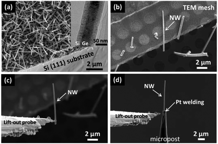 | ||
| Fig. 1 Procedure of preparing an individual NW for APT measurement. (a) NWs grown on a Si (111) substrate; the inset is a TEM image of a Ge/Si core–shell NW. (b) NWs transformed into a TEM mesh. (c) Picking up an individual NW from the TEM mesh using a lift-out probe. (d) Individual NW welded to a micropost. | ||
The procedure of preparing an individual NW for APT measurement is shown in Fig. 1. First, we dispersed the NWs into isopropyl alcohol (IPA) by placing the Si substrate (with NWs grown on it) into IPA and dripped IPA drops containing the NWs onto a TEM mesh [Fig. 1(b)]. Then, a NW was selected and picked up by a lift-out probe using a gallium (Ga) ion focused ion beam (FIB), and combined with an FIB-SEM dual-beam system (Helios NanoLab600i, FEI) [Fig. 1(c)]. Finally, the NW was welded onto a micropost for APT measurement [Fig. 1(d)].
APT analysis was performed using a laser-assisted local electrode atom probe (LEAP4000X HR, AMETEK).33,34 The NW was irradiated with a 355 nm-wavelength pulsed laser at a repetition rate of 100–200 kHz and a laser-pulse energy of 10–50 pJ. The base temperature during the measurement was 50 K. An integrated visualization and analysis software (IVAS) protocol was employed to reconstruct the 3D atomic maps.35
Results and discussion
Fig. 2(a) and (b) show 10 nm-thick atom maps of the side and top views of a Ge/Si core–shell NW, respectively. The Ge/Si core–shell structure can be observed from the atom maps, which show that the Ge core was covered by a Si shell, and B atoms were selectively doped into the Si shell. The entire Ge core and Si shell were not observed in Fig. 2(a) and (b) because of APT's limited field-of-view. For the specific APT equipment we employed, the field-of-view is limited to approximately 60 nm in diameter. However, the diameter of the Ge core could be up to 50 nm [as shown in the TEM image in Fig. 1(a)], so only the Ge core and a very thin Si shell could be detected if we measured the NW directly (see Fig. S1 in the ESI†). In order to observe the B distribution in the Si shell, we side milled halfway into a section of the NW using a Ga FIB (see Fig. S2 in the ESI†) before the measurement so that even a thick Si shell could be detected.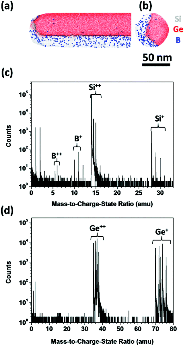 | ||
| Fig. 2 (a) Side- and (b) top-view atom maps of a Ge/Si core–shell NW (10 nm-thick slice). The 20 at% Si iso-concentration surface is also shown. Mass spectra of (c) Si shell and (d) Ge core regions. | ||
To determine whether the B atoms diffused into the Ge core, we compared the mass spectra of the Si shell and the Ge core, as shown in Fig. 2(c) and (d), respectively. B+ (10 and 11 amu) and B++ (5 and 5.5 amu) peaks clearly appeared in the mass spectrum of the Si shell, but neither B+ nor B++ peaks were observed in the Ge core, indicating that the B atoms did not diffuse into the Ge core. Given the extremely low diffusivity of B in Si at 700 °C (10−17 to 10−18 cm2 s−1),20 this result is reasonable.
Fig. 3(a) and (b) show the B distributions along the radial direction and the growth axis in a Ge/Si core–shell NW, respectively. Along the radial direction, the B atoms were randomly distributed in the Si shell. Furthermore, the B atoms were observed in the Ge/Si interface but not in the Ge core [Fig. 3(a)]. Because the additional Ge shell grown between the Ge core and the Si shell may not form perfect crystallinity, the Ge/Si interface could be rough, which would enable the B atoms to easily diffuse into the Ge/Si interface. Another reason may be that the APT resolution along the radial direction is lower than that along the axial direction, which introduces B atoms into the Ge/Si interface. In Fig. 3(b), the B atoms are randomly distributed along the growth axis and the average B concentration remains constant.
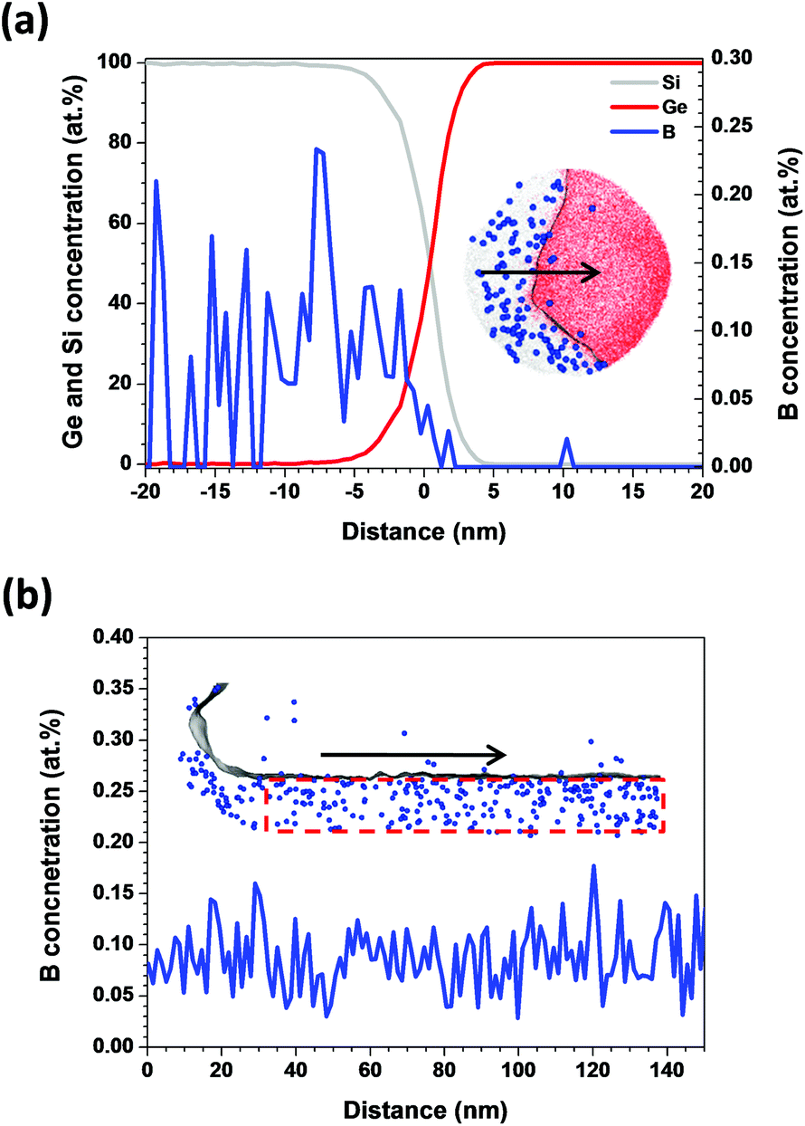 | ||
| Fig. 3 B concentration along (a) the radial direction and (b) the growth axis of a Ge/Si core–shell NW. The black arrows indicate the directions along which the B concentration was measured. | ||
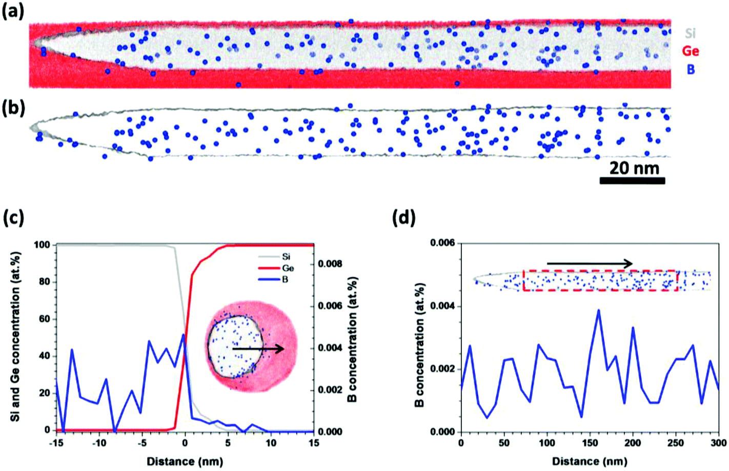
A Si/Ge core–shell NW was measured directly by APT without Ga ion milling. The atom map of the side view of a Si/Ge core–shell NW is shown in Fig. 4(a) (10 nm-thick slice), and the B-doped Si core was covered by a Ge shell. It was found that the Si core had a tapered shape, which resulted from vapor–solid (VS) deposition of Si on the sides of the Si core during growth. Because of the limited APT field-of-view mentioned above, only a thin Ge shell was detected, but this did not affect the investigation of the B distribution. In the B atom map shown in Fig. 4(b), it can be observed that the B atoms were segregated at the Si/Ge interface. A detailed analysis of the B distribution along the radial direction [Fig. 4(c)] indicated that the B atoms piled up in the outer region of the Si core and the B concentration decreased sharply from the outer region to the inner region. This is because B atoms were incorporated into the Si core not only via the VLS process but also via the VS process from the sidewall during the growth of the Si core. The B incorporation rate via VS is much higher than that via VLS, as reported previously,36 which caused a gradient in the B concentration along the radial direction. Moreover, as in the case of Ge/Si core–shell NWs, B atoms were not observed in the Ge shell, as shown in Fig. 4(b).
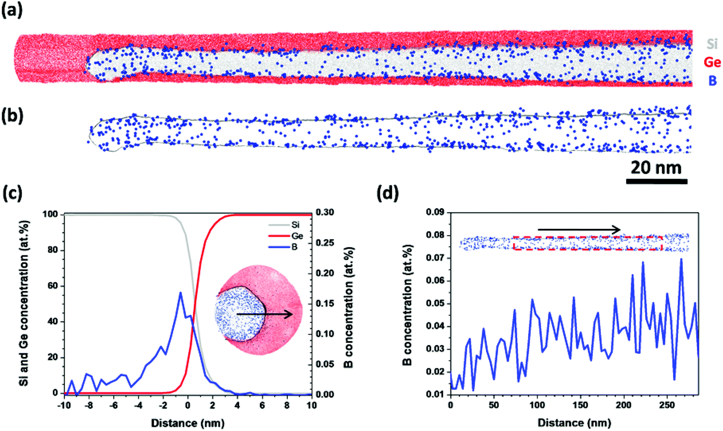 | ||
| Fig. 4 (a) Side-view atom map of a Si/Ge core–shell NW (10 nm-thick slice). The 20 at% Si iso-concentration surface is also shown. (b) B atom map of a Si/Ge core–shell NW. The B concentration along (c) the radial direction and (d) the growth axis of a Si/Ge core–shell NW. The black arrows in (c) and (d) indicate the directions along which the B concentration was measured. | ||
Along the growth axis, the average B concentration increased gradually from the top to the bottom of the NW [Fig. 4(d)]. This is due to the tapered shape of the Si core grown by the VS process. The exposure time of the Si core to the B2H6 source gas increased from the top to the bottom during the VS process, so the number of B atoms incorporated into the Si core from the sidewall increased from the top to the bottom of the NW. This was also observed in phosphorus-doped Ge NWs.15
The inhomogeneous distribution of B atoms in the Si core will affect the electrical properties of the NWs.19 Therefore, we prepared another kind of Si/Ge core–shell NW at a lower temperature and B2H6 flux, which was expected to eliminate B incorporation via the VS process.17,37,38Fig. 5(a) shows a 10 nm-slice atom map of a NW of this kind, in which the tapered shape was eliminated. B atoms were effectively doped into the Si core, and no obvious B pile-up was observed in the outer region of the Si core [Fig. 5(b)]. This was confirmed in a 1D concentration profile of B along the radial direction [Fig. 5(c)]. Furthermore, the average B concentration remained constant along the growth direction, as shown in Fig. 5(d).
 | ||
| Fig. 5 (a) Side-view atom map of a Si/Ge core–shell NW grown at low temperature and with a low B2H6 flux (10 nm-thick slice). The 20 at% Si iso-concentration surface is also shown. (b) B atom map in a Si/Ge core–shell NW. B concentration along (c) the radial direction and (d) the growth axis of a Si/Ge core–shell NW. The black arrows in (c) and (d) indicate the directions along which the B concentration was measured. | ||
A comparison of Fig. 4 and 5 indicated that B incorporation via the VS process from the sidewall of the Si core was suppressed by decreasing the growth temperature and B2H6 flux, which enabled us to obtain homogeneously B-doped Si/Ge core–shell NWs. The VS process relies on high temperatures to activate the chemical decomposition of precursor gases, and the deposition rate is proportional to the reciprocal temperature.39 Thus, the reduction in the growth temperature could decrease the rate of B incorporation via the VS process. In addition, as the precursor gases, SiH4 and B2H6, can form a polarized SiH4–BH3 complex that is easily adsorbed on the Si core surface,40,41 a high B2H6 flux could enhance the B incorporation rate, which has previously been reported for the CVD growth of B-doped Si and Ge thin films.38,42 Therefore, the rate of B incorporation from the sidewall of the Si core was reduced by decreasing the growth temperature and B2H6 flux.
Conclusions
The B distributions in Ge/Si and Si/Ge core–shell NWs were studied by APT. B atoms were precisely doped into the Si regions of Ge/Si and Si/Ge core–shell NWs, and did not diffuse into the Ge regions. In the Ge/Si core–shell NWs, the B atoms were randomly distributed along both the radial direction and the growth axis in the Si shell. On the other hand, in the Si/Ge core–shell NWs, the B distributions were controlled by the growth temperature and B2H6 flux. The B atoms piled up in the outer region of the Si core and the B concentration gradually increased from the top to the bottom of the NW along the growth axis when the growth temperature and B2H6 flux were higher. However, the B atoms were randomly distributed and the B concentration remained constant along the growth axis when the growth temperature and B2H6 flux were decreased.Acknowledgements
We would like to express thanks to Dr K. Yoshida for fruitful discussion and to Dr H. Takamizawa, Mr N. Ebisawa, Mrs K. Tomura, and Mrs Y. Nozawa for their technical support. This work was in part supported by JSPS KAKENHI grant numbers: 15H05413 and 26246021.References
- Y. Cui and C. M. Lieber, Science, 2001, 291, 851 CrossRef CAS PubMed.
- W. Lu and C. M. Lieber, Nat. Mater., 2007, 6, 841 CrossRef CAS PubMed.
- T. J. Kempa, R. W. Day, S.-K. Kim, H.-G. Park and C. M. Lieber, Energy Environ. Sci., 2013, 6, 719 CAS.
- B. Tian and C. M. Lieber, Annu. Rev. Anal. Chem., 2013, 6, 31 CrossRef CAS PubMed.
- M. Dutta, L. Thirugnanam, P. V. Trinh and N. Fukata, ACS Nano, 2015, 9, 6891 CrossRef CAS PubMed.
- L. J. Lauhon, M. S. Gudiksen, D. Wang and C. M. Lieber, Nature, 2002, 420, 57 CrossRef CAS PubMed.
- J. Xiang, A. Vidan, M. Tinkham, R. M. Westervelt and C. M. Lieber, Nat. Nanotechnol., 2006, 1, 208 CrossRef CAS PubMed.
- I. A. Goldthorpe, A. F. Marshall and P. C. McIntyre, Nano Lett., 2008, 8, 4081 CrossRef CAS PubMed.
- Y. Zhao, J. T. Smith, J. Appenzeller and C. Yang, Nano Lett., 2011, 11, 1406 CrossRef CAS PubMed.
- Y. Hu, J. Xiang, G. Liang, H. Yan and C. M. Lieber, Nano Lett., 2008, 8, 925 CrossRef CAS PubMed.
- J. Xiang, W. Lu, Y. Hu, Y. Wu, H. Yan and C. M. Lieber, Nature, 2006, 441, 489 CrossRef CAS PubMed.
- W. Lu, J. Xiang, B. P. Timko, Y. Wu and C. M. Lieber, Proc. Natl. Acad. Sci. U. S. A., 2005, 102, 10046 CrossRef CAS PubMed.
- N. Fukata, M. Yu, W. Jevasuwan, T. Takei, Y. Bando, W. Wu and Z. Wang, ACS Nano, 2015, 9, 12182 CrossRef CAS PubMed.
- T. Xu, J. P. Nys, B. Grandidier, D. Stiévenard, Y. Coffinier, R. Boukherroub, R. Larde, E. Cadel and P. Pareige, J. Vac. Sci. Technol., B, 2008, 26, 1960 CAS.
- D. E. Perea, E. R. Hemesath, E. J. Schwalbach, J. L. Lensch-Falk, P. W. Voorhees and L. J. Lauhon, Nat. Nanotechnol., 2009, 4, 315 CrossRef CAS PubMed.
- R. A. Schlitz, D. E. Perea, J. L. Lensch-Falk, E. R. Hemesath and L. J. Lauhon, Appl. Phys. Lett., 2009, 95, 162101 CrossRef.
- N. Fukata, K. Sato, M. Mitome, Y. Bando, T. Sekiguchi, M. Kirkham, J.-I. Hong and Z. L. Wang, ACS Nano, 2010, 4, 3807 CrossRef CAS PubMed.
- E. Koren, N. Berkovitch and Y. Rosenwaks, Nano Lett., 2010, 10, 1163 CrossRef CAS PubMed.
- M. V. Fernández-Serra, C. Adessi and X. Blase, Phys. Rev. Lett., 2006, 96, 166805 CrossRef PubMed.
- N. Fukata, M. Mitome, T. Sekiguchi, Y. Bando and M. Kirkham, ACS Nano, 2012, 6, 8887 CrossRef CAS PubMed.
- B. Han, H. Takamizawa, Y. Shimizu, K. Inoue, Y. Nagai, F. Yano, Y. Kunimune, M. Inoue and A. Nishida, Appl. Phys. Lett., 2015, 107, 023506 CrossRef.
- K. Inoue, H. Takamizawa, Y. Shimizu, F. Yano, T. Toyama, A. Nishida, T. Mogami, K. Kitamoto, T. Miyagi, J. Kato, S. Akahori, N. Okada, M. Kata, H. Uchida and Y. Nagai, Appl. Phys. Express, 2013, 6, 046502 CrossRef.
- Y. Shimizu, H. Takamizawa, Y. Kawamura, M. Uematsu, T. Toyama, K. Inoue, E. E. Haller, K. M. Itoh and Y. Nagai, J. Appl. Phys., 2013, 113, 026101 CrossRef.
- D. E. Perea, J. E. Allen, S. J. May, B. W. Wessels, D. N. Seidman and L. J. Lauhon, Nano Lett., 2006, 6, 181–185 CrossRef CAS PubMed.
- J. E. Allen, E. R. Hemesath, D. E. Perea, J. L. Lensch-Falk, Z. Y. Li, F. Yin, M. H. Gass, P. Wang, A. L. Bleloch, R. E. Palmer and L. J. Lincoln, Nat. Nanotechnol., 2008, 3, 168 CrossRef CAS PubMed.
- O. Moutanabbir, D. Isheim, H. Blumtritt, S. Senz, E. Pippel and D. N. Seidman, Nature, 2013, 496, 78 CrossRef CAS PubMed.
- J. R. Riley, R. A. Bernal, Q. Li, H. D. Espinosa, G. T. Wang and L. J. Lauhon, ACS Nano, 2012, 6, 3898 CrossRef CAS PubMed.
- N. Jeon, B. Loitsch, S. Morkoetter, G. Abstreiter, J. Finley, H. J. Krenner, G. Koblmueller and L. J. Lauhon, ACS Nano, 2015, 9, 8335 CrossRef CAS PubMed.
- H. Blumtritt, D. Isheim, S. Senz, D. N. Seidman and O. Moutanabbir, Nanotechnology, 2014, 25, 435704 CrossRef CAS PubMed.
- D. E. Perea, J. L. Lensch, S. J. May and L. J. Lauhon, Appl. Phys. A, 2006, 85, 271 CrossRef CAS.
- R. Agrawal, R. A. Bernal, D. Isheim and H. D. Espinosa, J. Phys. Chem. C, 2011, 115, 17688 CAS.
- C. M. Eichfeld, S. S. A. Gerstl, T. Prosa, Y. Ke, J. Redwing and S. E. Mohney, Nanotechnology, 2012, 23, 215205 CrossRef PubMed.
- T. F. Kelly, D. J. Larson, K. Thompson, R. L. Alvis, J. H. Bunton, J. D. Olson and B. P. Gorman, Annu. Rev. Mater. Res., 2007, 37, 681 CrossRef CAS.
- T. F. Kelly and D. J. Larson, Annu. Rev. Mater. Res., 2012, 42, 1 CrossRef CAS.
- F. Vurpillot, B. Gault, B. P. Geiser and D. J. Larson, Ultramicroscopy, 2013, 132, 19 CrossRef CAS PubMed.
- W. Chen, V. G. Dubrovskii, X. Liu, T. Xu, R. Lardé, J. Philippe Nys, B. Grandidier, D. Stiévenard, G. Patriarche and P. Pareige, J. Appl. Phys., 2012, 111, 094909 CrossRef.
- C. B. Jin, J. E. Yang and M. H. Jo, Appl. Phys. Lett., 2006, 88, 193105 CrossRef.
- E. Tutuc, S. Guha and J. O. Chu, Appl. Phys. Lett., 2006, 88, 043113 CrossRef.
- H. Kanoh, O. Sugiura, P. A. Breddels and M. Matsumura, Jpn. J. Appl. Phys., 1990, 29, 2358 CrossRef CAS.
- S. W. Hu, Y. Wang and X. Y. Wang, J. Phys. Chem. A, 2003, 107, 1635 CrossRef CAS.
- S. W. Hu, J. Kim, P. Tarakeshwar and K. S. Kim, J. Phys. Chem. A, 2002, 106, 6817 CrossRef CAS.
- L. H. Hall and K. M. Koliwad, J. Electrochem. Soc., 1973, 120, 1438 CrossRef CAS.
Footnote |
| † Electronic supplementary information (ESI) available. See DOI: 10.1039/c6nr04384d |
| This journal is © The Royal Society of Chemistry 2016 |