DOI:
10.1039/C6NR04335F
(Paper)
Nanoscale, 2016,
8, 14184-14192
Unidirectional light scattering with high efficiency at optical frequencies based on low-loss dielectric nanoantennas†‡
Received
29th May 2016
, Accepted 28th June 2016
First published on 29th June 2016
Abstract
Dielectric nanoparticles offer low optical losses and access to both electric and magnetic Mie resonances. This enables unidirectional scattering along the incident axis of light, owing to the interference between these two resonances. Here we theoretically and experimentally demonstrate that an asymmetric dimer of dielectric nanoparticles can provide unidirectional forward scattering with high efficiency. Theoretical analyses reveal that the dimer configuration can satisfy the first Kerker condition at the resonant peaks of electric and magnetic dipolar modes, therefore showing highly efficient directional forward scattering. The unidirectional forward scattering with high efficiency is confirmed in our experiments using a silicon nanodisk dimer on a transparent substrate. This study will boost the realization of practical applications using low-loss and efficient subwavelength all-dielectric nanoantennas.
1. Introduction
Controlling visible light with nanoparticles smaller than the wavelength has been subject of high interest in many applications; for instance, improving the efficiency of solar cells,1 increasing the sensitivity of optical sensors2,3 and realizing optical nanocircuits.4 Plasmonic nanoparticles made of noble metals have been demonstrated as a potential building block for nanoantennas able to control electromagnetic waves even below the diffraction limit.5,6 Coherent oscillations of free electrons in metallic nanoparticles, called localized surface plasmon resonances, are capable of confining the electric field into a subwavelength area, while at the same time resonantly enhancing scattering into the far field. However, substantial energy losses are inevitable, especially at visible light wavelengths, because of the presence of free electrons and their ohmic losses. This drawback has hampered the realization of the aforementioned applications using metallic plasmonic nanoparticles7 and stimulated the study of high-refractive-index dielectric nanoparticles as an alternative. For instance, dimers or oligomers of silicon nanostructures have been revealed to enhance and confine the electromagnetic field into the small gap, and to increase the scattering efficiency, without appreciable heat generation.8–16 These dielectric nanoantennas can be exploited, for example, by spectroscopic techniques such as fluorescence microscopy or surface enhance Raman scattering, where undesired heat could disturb the response of the sample.17
Furthermore, dielectric nanostructures possess not only electric but also magnetic resonances, even without considering complex shapes or arrangements.18–26 The magnetic resonances derive from the rotation of the displacement current inside the dielectric particles, showing a strong far-field scattering comparable to that of the electric modes.18–21 The presence of these magnetic resonances makes constructive and destructive interferences with the electric modes possible. At certain wavelengths, the electromagnetic wave can then be scattered from the dielectric nanoparticles selectively either in the forward direction, or in the backward direction.27–31 This unidirectional forward and backward scattering can be obtained when the first Mie coefficients a1 and b1 satisfy the equations a1 = b1 and a1 = −b1, respectively. These so-called Kerker conditions were proposed first with an ideal magnetic particle in 1983,32 then theoretically and experimentally examined using realistic dielectric materials recently with the expectation that this could open the path to realize high-performance directional low-loss nanoantennas.27–31 However, the scattering efficiency at the Kerker conditions is generally quite low for spherical particles. This is because the spherical dielectric particles have the electric and magnetic resonances with considerably large spectral separation in terms of resonant wavelength and intensity, and the Kerker conditions are fulfilled far from the resonant peaks.28,30 Heterodimer structure using gold and silicon nanospheres was investigated to enhance the scattering intensity with high directionality by interference between broad and narrow-band hybrid modes; however, the structure with metals still suffers from substantial ohmic losses.33 These losses could cause not only the reduction in scattering efficiency but also substantial heat which is undesirable for some spectroscopic applications.11,17 A theoretical study on dielectric spheroids and core–shell particles has revealed that tuning the aspect ratio of the spheroid or the core radius of the core–shell particle can shift the electric and magnetic dipole modes to the same resonant wavelengths.34–36 However, these structures are quite difficult to experimentally fabricate on the nanometer scale with fine precision. Dielectric nanodisks with low aspect ratio could be another possible candidate to obtain unidirectional forward scattering with high efficiency.31 However, in order to optimize resonant intensity and peak width, only adjusting the aspect ratio of the structure itself could be insufficient; for instance, relatively high refractive index substrate and surrounding media are reportedly required to optimize high transmittance.37
In this study, we investigate an asymmetric dimer configuration of dielectric nanoparticles, silicon in particular, as a novel solution to achieve directional scattering with high efficiency. The resonant wavelengths of dielectric nanostructures are tuneable by changing the dimension of the particles.18 Also previous studies revealed that dielectric dimers can offer strong coupling between the electric resonance excited in one particle and the magnetic one in the other if the two particles are placed close to each other.9,38 This study will use a detailed theoretical analysis based on an asymmetric dimer of spherical silicon nanoparticles to investigate the basic proof of concept of Kerker-like unidirectional forward scattering but with high scattering efficiency near the resonance. Furthermore, a practical configuration of a dimer of asymmetric silicon nanodisks on a transparent substrate will be used to experimentally demonstrate highly efficient unidirectional forward scattering of visible light from the nanoantenna. We will also discuss a design to obtain a multi-wavelength or broadband response by adding more finely tuned nanoparticles. The dielectric nanoantennas introduced in this paper could be a key unit constituting metasurfaces and nanometer scale devices such as efficient solar cells and optical sensors.
2. Methods
2.1 Numerical simulations
Numerical simulations were carried out using a FDTD solver (Lumerical) to calculate the optical responses of the silicon nanospheres in air and silicon nanodisks on a sapphire substrate. For nanospheres in air, a total-field scattered-field source with polarization parallel to the dimer axis was used to calculate the field scattered to the forward and backward hemispheres. For nanodisks on a sapphire substrate, we combined two Gaussian beams the phase of which were reversed to obtain a dark field beam source with polarization parallel to the dimer axis. The scattered field was integrated on the far field hemispheres with a collection angle below 53°, which corresponds to the objective lens of NA 0.8 used in the experiment. Scattering efficiency was calculated by dividing integrated scattered power by the dark field source power. This setting for the disk case enables us to compare numerical and experimental results. In the gap of the dimer, the mesh size was refined to 0.5 nm and 2 nm in the case of the sphere dimer in air and the disk dimer on substrate, respectively, to ensure convergence of results.
2.2 Theoretical analyses
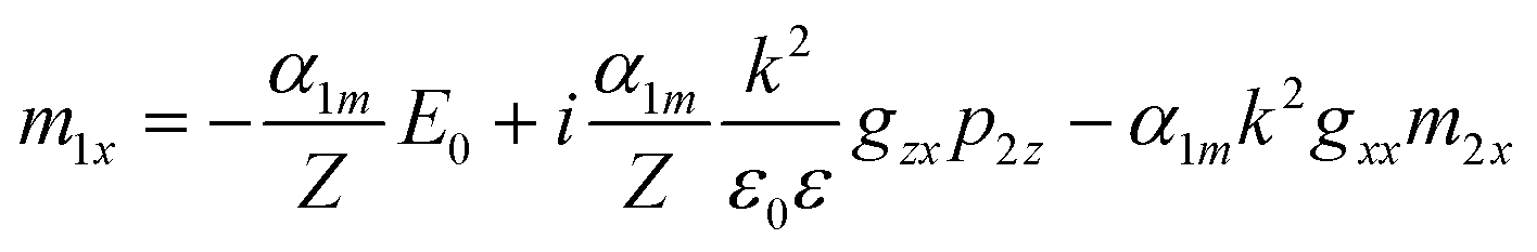
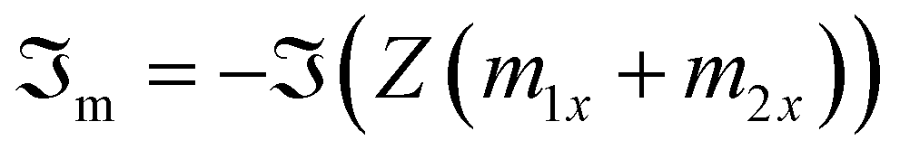
Details of the analytical dipole–dipole model are given in our previous papers.9,39 Briefly, when a plane wave illuminates the dimer with electric polarization along to the dimer axis (p-polarization), the electric and magnetic dipolar resonances excited in the particle are| | | p1y = ε0εα1eE0 + α1ek2gyyp2y | (1) |
| | | p2y = ε0εα2eE0 + α2ek2gyyp1y | (2) |
| | | p1z = −α1ek2gxxp2z + iε0εα1eZk2gzxm2x | (3) |
| | | p2z = −α2ek2gxxp1z + iε0εα2eZk2gzxm1x | (4) |
| |  | (5) |
| |  | (6) |
where pjy and pjz are the electric dipole moments excited in the jth (j = 1, 2) particle along the y-axis and z-axis, respectively, mjx is a magnetic dipole moment along the x-axis, ε0 is the vacuum permittivity, ε is the relative permittivity of the loss-less media, E0 is the incident electric field, k is the wavenumber in vacuum, Z is the vacuum impedance, αje and αjm are the electric and magnetic polarizability of the jth particle, and gyy, gxx and gzx are the scalar green functions. The components of the electric and magnetic dipoles in the two particles are given by the solution of these equations.
2.3 Fabrication of silicon nanoparticles on a sapphire substrate
Silicon single disks and dimers were fabricated by electron beam lithography using an epitaxially grown silicon-on-sapphire substrate with a polished backside. The substrate was coated with positive tone resist PMMA (poly(methyl methacrylate)) and baked at 180 °C for 2 minutes. Exposure was followed by a development procedure with MIBK (methyl isobutyl ketone)![[thin space (1/6-em)]](https://www.rsc.org/images/entities/char_2009.gif) :IPA (isopropanol) = 1:3 solution. Then a 40 nm Cr thin layer was deposited by thermal evaporation, followed by lift-off process with acetone solution. Subsequently the pattern was transferred to the silicon layers using reactive ion etching with the Cr nanostructures as a mask. The Cr mask was removed with commercial Cr etchant solution to obtain the final sample. Each nanoantenna was separated at a distance of 5 μm for single antenna measurement.
:IPA (isopropanol) = 1:3 solution. Then a 40 nm Cr thin layer was deposited by thermal evaporation, followed by lift-off process with acetone solution. Subsequently the pattern was transferred to the silicon layers using reactive ion etching with the Cr nanostructures as a mask. The Cr mask was removed with commercial Cr etchant solution to obtain the final sample. Each nanoantenna was separated at a distance of 5 μm for single antenna measurement.
2.4 Dark field scattering measurement of single nanoantennas
The scattered field from the silicon nanoantennas was collected using an optical dark field microscope (Nikon, Ti-U) equipped with a Xe lamp, spectrometer and charge-coupled device (CCD) camera. The incident light was illuminated from a dark field objective with an incident angle θi = 60–70°. The incident light was polarized parallel to the dimer axis by a linear polarizer placed on the light path. The polarization direction was confirmed by inserting another polarizer right over the fabricated sample. In the case of forward scattering, another dark field objective set below the sample collected the scattered field (Fig. 1a). Backward scattering was detected by the same dark field objective used for illumination (Fig. 1b). The NA of the objectives for light illumination and collection was 0.8, which corresponds to a maximum collection angle of θs = 53°. The signal from the sample was normalized by a flat pellet of barium sulfate fine powder after being subtracted by the signal from the substrate without any particle.
 |
| | Fig. 1 Schematic images of the optical measurement setup. Detailed illustration of the darkfield single nanoantenna measurement setups for the forward scattering (a) and backward scattering (b). | |
3. Results and discussion
3.1 Numerical and theoretical analysis of an asymmetric silicon spherical dimer
We first numerically investigated an asymmetric dimer of silicon spherical nanoparticles in air using the finite-element time-domain (FDTD) simulation method and an analytical dipole–dipole model developed in previous works9,39 to verify the achievement of the Kerker condition in the dimer case. Note that the spherical nanoparticles were used in this section since the full Mie theory can be applied giving us the exact solution of the resonant modes.
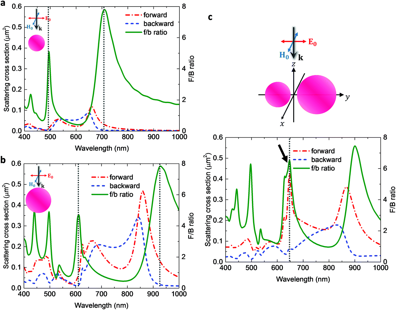
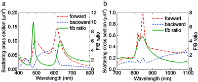
Fig. 2a–c show numerical results of the scattering spectra to the forward and backward direction and their ratio (F/B ratio) for single and dimer configurations. Two silicon spherical nanoparticles, whose diameters were 165 nm and 225 nm, were placed in air forming a dimer. For the theoretical analysis, we first used a separation distance of 5 nm to obtain strong coupling between the two particles. This dimer was illuminated by a plane wave polarized parallel to the dimer axis. Two broad peaks were observed around λ = 530 nm and 660 nm, and around λ = 660 nm and 860 nm in the scattering spectra, which correspond to the electric and magnetic dipolar resonances of the small and large particles, respectively. The scattering peaks observed at shorter wavelengths than the dipolar modes were attributed to higher-order mode resonances. In the F/B ratio spectra of the single spheres, two peaks were observed at wavelengths shorter than the electric dipole resonance and longer than magnetic dipole resonance, at which the first Kerker condition was achieved. However, the scattering efficiency to the forward direction at those wavelengths was very low, as reported previously, since the Kerker condition occurs away from the resonance peaks.28,30 The asymmetric dimer structure, on the other hand, showed a distinct new peak in its F/B ratio spectrum around λ = 650 nm, at which the forward scattering presented a peak and backward scattering was suppressed. This demonstrates unidirectional scattering to the forward direction with high scattering efficiency using the asymmetric dimer configuration. The wavelength showing this unidirectional scattering was close to the wavelength at which the magnetic dipolar resonance in the small particle and the electric dipolar resonance in the large are excited.
 |
| | Fig. 2 Configuration and results of the FDTD simulation. (a–c) Spectra of scattering cross section to the forward and backward direction and F/B ratio of the 165 nm diameter single sphere (a), the 225 nm diameter single sphere (b) and the dimer of these spheres (c). Insets are configurations used in the calculation. | |
The other peaks in the F/B ratio spectra of the dimer configuration derive from the response of each individual particle; for example, the peak of F/B ratio at λ = 900 nm of the dimer structure agrees well with that at λ = 925 nm of the large single particle. The scattering efficiencies at these wavelengths, however, were low compared to the new peak around λ = 650 nm. Please note that we integrated the scattered field throughout hemispheres in the forward and backward direction to calculate the scattering efficiencies and F/B ratio since this condition is close to the experimental demonstration described below. A previous theoretical work showed that a single silicon nanodisk which has diameter of 620 nm and thickness of 220 nm exhibited more than 103 front to back ratio at NIR wavelengths.31 However, that number was calculated with an ideal point dipolar source and considering a singular forward and backward direction point (270° and 90° respectively). When the structure was illuminated by a plane (or Gaussian) wave, and the scattered light was collected throughout both hemispheres in the far field, the nanodisk exhibited a F/B ratio of around 8 (see Fig. S1 in ESI†). This F/B ratio is comparable with those of the single spheres and the dimer shown in Fig. 1 given the same calculation method is used.
Fig. 3a shows the cross-section of radiation patterns of the scattered field on x–z plane at the wavelengths of maximum F/B ratios. The scattering intensity of the dimer in the 270° direction, which corresponds to direct forward scattering, was more than 10 times larger than those of single spheres. This enhancement in intensity clearly showed the advantage of the asymmetric dimer which can fully utilize the scattering resonance for unidirectional forward scattering. A small fraction of scattering to the backward direction was also observed in the far-field distribution of the dimer, possibly due to the presence of magnetic quadrupoles excited near the electric dipolar response of the larger sphere. The far field patterns on the y–z plane are shown in Fig. S2,† where the higher scattering intensity of the dimer was also confirmed. The electric field in the y–z plane was monitored at λ = 647 nm (Fig. 3b) to explore the resonances excited in the dimer. The typical rotation and oscillation of the displacement current, which correspond to the magnetic and electric resonances respectively, were observed in the small and large spheres. The electric resonance in the large particle showed not only an y-component but also a z-component, since an electric resonance along to the z-axis was induced by the interaction with the magnetic resonance of the small particle.9 Intense confinement and enhancement of the electric field was generated in the gap, suggesting the presence of coupling between the electric and magnetic near-field dipolar resonances of each particle. The hot spot generated at the gap introduces another key advantage of this asymmetric dimer over the single disk configuration. As reported,9–12,17 the hot spot of dielectric nanodimers can be applied to surface enhanced spectroscopic applications. In fact, we would expect that combining the highly efficient unidirectional forward scattering with the hot spot generated at the gap of the dimer could open up the path to highly sensitive spectroscopic applications in nanometer scale.
 |
| | Fig. 3 (a) Scattering pattern in far field from the single spheres and dimer configuration projected in x–z plane. (b) Electric field intensity and coupling between the resonances. Cross section of electric field intensity inside and near the dimer configuration at 647 nm illumination in the y-z plane. White arrows in the figure show the real part of electric field vectors at each calculation cell. | |
To verify the achievement of the first Kerker condition, we analyzed the dimer configuration using an analytical dipole–dipole model described in detail in ref. 9 and 39. The electric and magnetic dipoles excited perpendicular to the incident axis in the small (p1y and m1x) and large (p2y and m2x) nanoparticles contribute to the directional scattering along the incident axis. The first Kerker condition can be fulfilled when the Mie coefficients of electric and magnetic dipolar resonances are equal. The contribution of the electric and magnetic dipoles both in real and imaginary parts are calculated as follows,
| |  | (7) |
| |  | (8) |
| |  | (9) |
| |  | (10) |
where
ε0 is the vacuum permittivity,
ε is the relative permittivity of the lossless media, and
Z is the vacuum impedance. In order to achieve the first Kerker condition, we need to satisfy the following.
The real and imaginary part of the electric and magnetic dipolar resonances were plotted in Fig. 4. The eqn (11) and (12) were satisfied around 650 nm at which unidirectional forward scattering was observed in the FDTD numerical simulation. This agreement strongly suggest that the first Kerker condition was achieved with the asymmetric dimer configuration around 650 nm, at which the resonant scattering peak was also observed. Note that the analytical dipole–dipole model we used includes all the possible dipolar couplings (electric-electric, magnetic-magnetic and electric-magnetic).9,39 As shown in Fig. 3b, the electric–magnetic coupling was dominant and contributed most to the unidirectional forward scattering.
 |
| | Fig. 4 Theoretical analysis using the dipole–dipole model. The real and imaginary part of the electric and magnetic dipolar resonances excited in the dimer configuration calculated using the analytical dipole–dipole model. | |
We now compare our asymmetric dimer configuration with a symmetric one, which exhibits a directional Fano-like resonance. This resonance can be obtained in the symmetric silicon dimer structure due to the interaction between the sharp magnetic dipolar resonance and the electric dipolar resonance broadened by strong coupling between the two particles.13 This strong coupling is possible only when the two particles are placed very close to each other.9 The scattering and F/B ratio spectra of an asymmetric dimer of 165 nm and 225 nm diameter silicon spherical nanoparticles and of a symmetric dimer of 165 nm diameter nanoparticles are shown in Fig. 5a–d, for gap of 5 nm or 20 nm. With the smaller gap, the forward scattering cross section has a resonant peak at 647 nm for the asymmetric dimer, and at 657 nm for the symmetric one. The F/B ratio at the resonant maximum was almost the same between the two configurations. However, the situation changed significantly when the gap separation is increased to 20 nm. Both the forward scattering and the F/B ratio spectra of the asymmetric dimer showed little change even for the larger gap. In contrast, the maximum forward scattering efficiency of the symmetric dimer dropped by 12%, and the forward scattering and F/B ratio peaks were shifted, showing more separation from each other. Fig. 5e shows the F/B ratio at the forward scattering maximum as a function of the gap separation distance for both dimers. As the gap increased, the F/B ratio of the symmetric dimer structure dropped more rapidly than that of the asymmetric one. In addition, the maximum of forward scattering efficiency also showed a drop only in the case of symmetric dimer (Fig. 5f, also see Fig. S3 in ESI†). These differences in behaviour with gap size are due to the fact that strong coupling is necessary to achieve a Fano resonance owing to the broadening of the electric mode. However, the fulfilment of the Kerker condition requires only the overlap of the independent electric and magnetic resonances and, therefore, becomes less dependent on the coupling amplitude. These results would make the asymmetric dimer superior to the symmetric one for practical applications since gap sizes are not so critical in the Kerker case, enabling realization with less demanding lithography.
 |
| | Fig. 5 Comparison between Kerker-like asymmetric and Fano-like symmetric dimer structures. (a, b) Spectra of scattering cross section to the forward and backward direction and F/B ratio of the asymmetric dimer (a) and symmetric dimer (b) with the gap separation of 5 nm. (c, d) Spectra of the asymmetric dimer (c) and symmetric dimer (d) with the gap separation of 20 nm. (e, f) F/B ratio (e) and forward scattering efficiency (f) as a function of the gap separation of asymmetric (black, solid line, full square) and symmetric (red, broken line, open circle) dimers. | |
Also note that the wavelength of the electric and magnetic resonances generated in dielectric particles is tuneable by changing the dimension of the nanoparticles. As an example, we show in Fig. 6 the calculated scattering and F/B spectra of a dimer with silicon spherical particles of 110 nm and 150 nm diameter (Fig. 6a), and of 225 nm and 310 nm diameter (Fig. 6b), both with a gap separation of 5 nm. Efficient unidirectional forward scattering was confirmed as well around λ = 480 nm and λ = 860 nm, which were shifted from λ = 650 nm in the former dimer case due to the change in the dimension of the nanoparticles. Furthermore, the rescalability of highly efficient unidirectional scattering is not restricted to the optical regime. It is well known that the scattering properties of a dielectric object are fully scalable with identical properties from DC to light as long as the size parameter of the object is the same.28,40,41 Therefore, the concept introduced in this study of using asymmetric dimer can be used from the optical to the microwave regime.
 |
| | Fig. 6 Scattering properties shifted to the boundaries of the visible regime. Spectra of scattering cross sections to the forward and backward directions and F/B ratio of the dimer using silicon spheres of 110 nm and 150 nm diameter (a) and the dimer using silicon spheres of 225 nm and 310 nm diameter (b). | |
3.2 Experimental demonstration of the unidirectional scattering from asymmetric silicon dimers
We fabricated dimers of silicon nanodisks on transparent sapphire substrates using a lithography method described in detail in the Method section.
Insets of Fig. 7a–c show the SEM images of a fabricated nanodisk dimer and isolated single nanodisks. From the top side, the shape of the structures was almost an exact circle and the gap of the dimer was clear without any residuals. The lateral view of the fabricated dimer showed that the side wall of the disks vertically reached the surface of the substrate. The diameters of the disks were 125 nm and 155 nm for the small and large particles respectively, both with a thickness of 220 nm. These parameters were chosen for the disks because a high aspect ratio favours for the electric and magnetic dipolar resonances to be well separated,42 and hence suitable to study the overlap of the electric dipolar resonance of one particle and the magnetic resonance of the other. The gap of the dimer structure was around 20 nm, which is close to the resolution limit of our electron beam lithography equipment.
 |
| | Fig. 7 Experimentally measured scattering properties and comparison with simulations. (a–c) Scattering spectra to the forward and backward directions obtained in dark field single nanoantenna measurements of a single disk of 125 nm diameter (a), a single disk of 155 nm diameter (b) and the dimer of these two disks (c). (inset) SEM images of the fabricated samples with a scale bar of 100 nm. (d–f) Scattering spectra to the forward and backward directions and the F/B ratio calculated using the FDTD method. | |
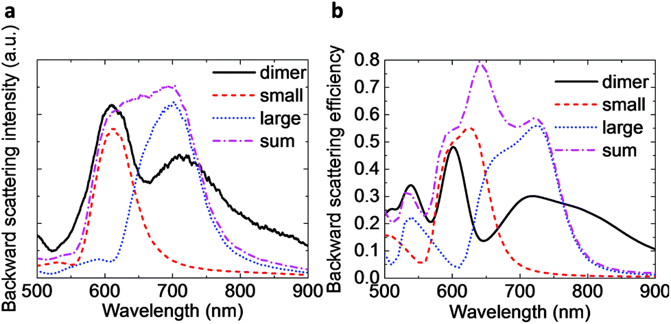
To experimentally confirm the directional forward scattering, we conducted nanoparticle dark field spectroscopy measurements for the single and dimer disks into the forward and backward scattering directions. The experimental setup is described in detail in the Methods section. In Fig. 7, we show the forward and backward scattering spectra obtained in the experiment (a–c) and compare with numerical simulation (d–f). The forward scattering spectra of the single disks have two resonant peaks at λ = 585 nm and λ = 623 nm for the small disk, and λ = 642 nm and λ = 718 nm for the large one. Their backward scattering spectra, which have peaks at λ = 613 nm and λ = 703 nm for the small and large disks, respectively, showed no clear dip around the wavelengths of the forward scattering peaks. In the dimer spectra, however, the largest forward scattering peak was observed around λ = 660 nm, at which the backward scattering was clearly suppressed. This result shows that preferential forward scattering was achieved with high forward scattering efficiency only for the dimer configuration.
A numerical study based on the FDTD method was carried out to analyze and interpret the experimental findings (Fig. 7d–f). The experimentally obtained scattering spectra agreed well with those numerically calculated. The spectra of the single disks presented high F/B ratios at wavelengths shorter than the electric dipolar resonances and longer than the magnetic ones. However, the directional forward scattering was achieved away from any resonant peaks and the forward scattering intensity was low, as well as in the single sphere case. In the asymmetric dimer case, in contrast, the peak of the forward scattering and the dip of the backward scattering were observed at the same wavelength around λ = 650 nm, leading to the high F/B ratio with strong forward scattering. These results showed that placing the two disks in a proximity to get strong coupling between the electric and magnetic dipolar resonance resulted in increasing the scattering efficiency and at the same time in improving the F/B ratio. Note that the calculated F/B ratio was lower than in the sphere case. The increase in the incident angle caused the reduction in the F/B ratio because disks on a substrate do not have a perfect symmetry like spheres in air. The illumination from a wide incident angle, hence, could cause the distortion in the resonances, disturbing the coupling between the two nanoparticles. When incident light is normal or close to normal to the substrate, the F/B ratio increases significantly and can reach values of around 15 (see Fig. S4 in ESI†).
The experimental results only showed minor differences when compared to the simulations. The small differences can be attributed to the imperfectness of the fabricated structures. We conducted the same measurement with other dimers, which revealed small differences amongst each other in the shape of the spectra but the clear reproducibility of the unidirectional forward scattering and some small peaks which agreed well with the spectra obtained in the simulation (see Fig. S5 in ESI†).
Backward scattering spectra were also compared in detail between single and dimer disks. In the spectra obtained experimentally (Fig. 8a), there was no dip observe d just by summing the spectra of single disks, while a clear dip of the backward scattering appeared in the dimer spectrum around λ = 660 nm. The backward scattering spectra obtained in the simulation are plotted in Fig. 8b, showing a similar tendency, and confirming that only the dimer structure has a dip around 650 nm. This comparison suggests that the suppression of backward scattering and directional forward scattering can be obtained with the dimer configuration where strong coupling between the electric and magnetic dipole in each particle is observed. Note that the unidirectional forward scattering with the dimer of silicon nanodisks on a substrate is also spectrally scalable similarly to the sphere case. The electric and magnetic dipolar resonance can be tuned simply by changing the height and/or diameter of the disk shape.43
 |
| | Fig. 8 Comparison of experimental (a) and theoretical (b) scattering spectra to the backward direction of the single disks, the numerical sum of these two disks and the dimer configuration. | |
The theoretical analysis and experimental demonstration with the dimer of nanospheres and high-aspect ratio nanodisks showed that the concept of using asymmetric dimer for unidirectional forward scattering with high efficiency is not restricted by the shape of the nanoparticles. The proposed idea could be applied to any arbitrary shapes including spheres, spheroids, high or low aspect ratio disks and rectangles.
3.3 Expansion of the idea for multi-wavelength and broadband response
The dimer configuration showed unidirectional forward scattering with high scattering efficiency at a certain wavelength that can be tuned with the particle size ratio. However, other applications such as solar cells and lighting instruments may require multi-wavelengths or broadband responses to improve their performance. In order to extend the wavelength range which shows unidirectional forward scattering, a trimer configuration was also explored. As an example, three silicon spheres aligned in line with diameter of 165 nm, 225 nm, and 310 nm and a gap of 5 nm between each particle were investigated with FDTD simulations using incident light with polarization parallel to the trimer axis (Fig. 9a). We chose these three diameters to obtain the overlapping between the electric and magnetic dipolar resonances at two different wavelengths in visible regime as shown in Fig. 2c and 6b. Fig. 9b shows forward and backward scattering spectra from the trimer and their F/B ratio. Large F/B ratios were obtained around λ = 650 nm and λ = 850 nm, where the forward scattering also showed resonant peaks. This result shows that the proposed asymmetric configurations are not limited to one wavelength, but can be extend to multi-wavelengths resonances. Note that the multi-wavelength response obtained in this study is distinguishable from previous works where the oligomer configuration was used for highly directional nanoantennas based on Yagi-Uda like structures.44–46 The oligomer proposed here consists of nanoparticles which are designed to provide more overlapping between electric and magnetic modes throughout the desired range of wavelength and, hence, could reach a broadband unidirectional forward scattering with high efficiency.
 |
| | Fig. 9 (a) Schematic image of the configuration used in calculation. (b) Scattering spectra of the trimer. Scattering cross section to the forward and backward direction and F/B ratio of the trimer using silicon spheres of 165 nm, 225 nm and 310 nm diameter. | |
4. Conclusions
We revealed that highly efficient unidirectional forward scattering can be obtained using dimers of asymmetric silicon nanoparticles (spherical or cylindrical). Theoretical and numerical analyses of the spherical dimer showed that this configuration is capable of scattering light to the forward direction selectively with high efficiency by fulfilling the first Kerker condition between the electric dipolar resonance excited in one particle and the magnetic in the other. This unidirectional scattering was experimentally confirmed by dark field scattering measurements with a dimer of asymmetric silicon disks on a sapphire substrate. Our study shows that finely tuned and aligned dielectric nanoparticles act as low-loss nanoantennas which can route light with high efficiency, and hence boost the realization of practical metasurface and nanometer scale devices using optical subwavelength nanoantennas. Also, the presence of the hot spot, when coupled to the highly efficient unidirectional forward scattering demonstrated in this work, could help improve existing spectroscopic techniques.
Acknowledgements
The authors acknowledge funding provided by grants the EPSRC Reactive Plasmonics Programme EP/M013812/1, the Leverhulme Trust (UK), the Royal Society ONR Global, and the US Army Transatlantic Research Office. The authors kindly acknowledge M. Rahmani for helping with the fabrication of samples and T. Roschuk for helping with the optical measurement setup. S. A. M. further acknowledges the Lee-Lucas Chair and Royal Society.
References
- H. A. Atwater and A. Polman, Nat. Mater., 2010, 9, 205–213 CrossRef CAS PubMed.
- S. M. Nie and S. R. Emery, Science, 1997, 275, 1102–1106 CrossRef CAS PubMed.
- P. J. Tarcha, J. DeSaja-Gonzalez, S. Rodriguez-Llorente and R. Aroca, Appl. Spectrosc., 1999, 53, 43–48 CrossRef CAS.
- N. Engheta, Science, 2007, 317, 1698–1702 CrossRef CAS PubMed.
-
S. Maier, Plasmonics: fundamentals and applications, Springer, New York, 2007 Search PubMed.
- D. K. Gramotnev and S. I. Bozhevolnyi, Nat. Photonics, 2010, 4, 83–91 CrossRef CAS.
- J. B. Khurgin, Nat. Nanotechnol., 2015, 10, 2–6 CrossRef CAS PubMed.
- M. M. Sigalas, D. A. Fattal, R. S. Williams, S. Y. Wang and R. G. Beausoleil, Opt. Express, 2007, 15, 14711–14716 CrossRef CAS PubMed.
- P. Albella, M. A. Poyli, M. K. Schmidt, S. A. Maier, F. Moreno, J. J. Saenz and J. Aizpurua, J. Phys. Chem. C, 2013, 117, 13573–13584 CAS.
- R. M. Bakker, D. Permyakov, Y. F. Yu, D. Markovich, R. Paniagua-Dominguez, L. Gonzaga, A. Samusev, Y. Kivshar, B. Luk'yanchuk and A. I. Kuznetsov, Nano Lett., 2015, 15, 2137–2142 CrossRef CAS PubMed.
- P. Albella, R. A. de la Osa, F. Moreno and S. A. Maier, ACS Photonics, 2014, 1, 524–529 CrossRef CAS.
- J. van de Groep, T. Coenen, S. A. Mann and A. Polman, Optica, 2016, 3, 7 Search PubMed.
- J. H. Yan, P. Liu, Z. Y. Lin, H. Wang, H. J. Chen, C. X. Wang and G. W. Yang, ACS Nano, 2015, 9, 2968–2980 CrossRef CAS PubMed.
- J. H. Yan, P. Liu, Z. Y. Lin, H. Wang, H. J. Chen, C. X. Wang and G. W. Yang, Nat. Commun., 2015, 6, 7042 CrossRef CAS PubMed.
- A. E. Miroshnichenko and Y. S. Kivshar, Nano Lett., 2012, 12, 6459–6463 CrossRef CAS PubMed.
- K. E. Chong, B. Hopkins, I. Staude, A. E. Miroshnichenko, J. Dominguez, M. Decker, D. N. Neshev, I. Brener and Y. S. Kivshar, Small, 2014, 10, 1985–1990 CrossRef CAS PubMed.
- M. Caldarola, P. Albella, E. Cortes, M. Rahmani, T. Roschuk, G. Grinblat, R. F. Oulton, A. V. Bragas and S. A. Maier, Nat. Commun., 2015, 6, 7915 CrossRef CAS PubMed.
- A. B. Evlyukhin, C. Reinhardt, A. Seidel, B. S. Luk'yanchuk and B. N. Chichkov, Phys. Rev. B: Condens. Matter, 2010, 82, 12 CrossRef.
- A. Garcia-Etxarri, R. Gomez-Medina, L. S. Froufe-Perez, C. Lopez, L. Chantada, F. Scheffold, J. Aizpurua, M. Nieto-Vesperinas and J. J. Saenz, Opt. Express, 2011, 19, 4815–4826 CAS.
- A. B. Evlyukhin, S. M. Novikov, U. Zywietz, R. L. Eriksen, C. Reinhardt, S. I. Bozhevolnyi and B. N. Chichkov, Nano Lett., 2012, 12, 3749–3755 CrossRef CAS PubMed.
- A. I. Kuznetsov, A. E. Miroshnichenko, Y. H. Fu, J. B. Zhang and B. Luk'yanchuk, Sci. Rep., 2012, 2, 6 Search PubMed.
- M. K. Schmidt, R. Esteban, J. J. Saenz, I. Suarez-Lacalle, S. Mackowski and J. Aizpurua, Opt. Express, 2012, 20, 13636–13650 CrossRef CAS PubMed.
- A. B. Evlyukhin, R. L. Eriksen, W. Cheng, J. Beermann, C. Reinhardt, A. Petrov, S. Prorok, M. Eich, B. N. Chichkov and S. I. Bozhevolnyi, Sci. Rep., 2014, 4, 7 Search PubMed.
- G. Boudarham, R. Abdeddaim and N. Bonod, Appl. Phys. Lett., 2014, 104, 4 CrossRef.
- Z.-Y. Jia, J.-N. Li, H.-W. Wu, C. Wang, T.-Y. Chen, R.-W. Peng and M. Wang, J. Appl. Phys., 2016, 119, 074302 CrossRef.
- A. E. Krasnok, C. R. Simovski, P. a. Belov and Y. S. Kivshar, Nanoscale, 2014, 6, 7354–7361 RSC.
- M. Nieto-Vesperinas, R. Gomez-Medina and J. J. Saenz, J. Opt. Soc. Am. A, 2011, 28, 54–60 CrossRef CAS PubMed.
- J. M. Geffrin, B. Garcia-Camara, R. Gomez-Medina, P. Albella, L. S. Froufe-Perez, C. Eyraud, A. Litman, R. Vaillon, F. Gonzalez, M. Nieto-Vesperinas, J. J. Saenz and F. Moreno, Nat. Commun., 2012, 3, 8 Search PubMed.
- S. Person, M. Jain, Z. Lapin, J. J. Saenz, G. Wicks and L. Novotny, Nano Lett., 2013, 13, 1806–1809 CrossRef CAS PubMed.
- Y. H. Fu, A. I. Kuznetsov, A. E. Miroshnichenko, Y. F. Yu and B. Luk'yanchuk, Nat. Commun., 2013, 4, 6 Search PubMed.
- I. Staude, A. E. Miroshnichenko, M. Decker, N. T. Fofang, S. Liu, E. Gonzales, J. Dominguez, T. S. Luk, D. N. Neshev, I. Brener and Y. Kivshar, ACS Nano, 2013, 7, 7824–7832 CrossRef CAS PubMed.
- M. Kerker, D. S. Wang and C. L. Giles, J. Opt. Soc. Am., 1983, 73, 765–767 CrossRef.
- H. Wang, P. Liu, Y. L. Ke, Y. K. Su, L. Zhang, N. S. Xu, S. Z. Deng and H. J. Chen, ACS Nano, 2015, 9, 436–448 CrossRef CAS PubMed.
- B. S. Luk'yanchuk, N. V. Voshchinnikov, R. Paniagua-Domínguez and A. I. Kuznetsov, ACS Photonics, 2015, 2, 150616161431005 Search PubMed.
- W. Liu, J. Zhang, B. Lei, H. Ma, W. Xie and H. Hu, Opt. Express, 2014, 22, 16178 CrossRef PubMed.
- R. R. Naraghi, S. Sukhov and A. Dogariu, Opt. Lett., 2015, 40, 585–588 CrossRef PubMed.
- M. Decker, I. Staude, M. Falkner, J. Dominguez, D. N. Neshev, I. Brener, T. Pertsch and Y. S. Kivshar, Adv. Opt. Mater., 2015, 3, 813–820 CrossRef CAS.
- U. Zywietz, M. K. Schmidt, A. B. Evlyukhin, C. Reinhardt, J. Aizpurua and B. N. Chichkov, ACS Photonics, 2015, 2, 913–920 CrossRef CAS.
- P. Albella, T. Shibanuma and S. A. Maier, Sci. Rep., 2015, 5, 8 Search PubMed.
- D. S. Filonov, A. E. Krasnok, A. P. Slobozhanyuk, P. V. Kapitanova, E. A. Nenasheva, Y. S. Kivshar and P. A. Belov, Appl. Phys. Lett., 2012, 100, 4 CrossRef.
- B. Rolly, J. M. Geffrin, R. Abdeddaim, B. Stout and N. Bonod, Sci. Rep., 2013, 3, 5 Search PubMed.
- P. Moitra, B. A. Slovick, Z. G. Yu, S. Krishnamurthy and J. Valentine, Appl. Phys. Lett., 2014, 104, 5 CrossRef.
- J. van de Groep and A. Polman, Opt. Express, 2013, 21, 26285–26302 CrossRef CAS PubMed.
- A. E. Krasnok, A. E. Miroshnichenko, P. A. Belov and Y. S. Kivshar, JETP Lett., 2011, 94, 593–598 CrossRef CAS.
-
A. E. Krasnok, A. E. Miroshnichenko, P. A. Belov and Y. S. Kivshar, in 5th International Workshop on Theoretical and Computational Nano-Photonics (TaCoNa-Photonics), Amer Inst Physics, MELVILLE, 2012, vol. 1475, pp. 22–24.
- B. Rolly, B. Stout and N. Bonod, Opt. Express, 2012, 20, 20376–20386 CrossRef PubMed.
Footnotes |
| † Electronic supplementary information (ESI) available: F/B ratio of the optimized single disk; comparison between the asymmetric and symmetric dimer with 30 nm gap; far field patterns on the y-z plane correlation between incident angle and F/B ratio; scattering spectra of nanodisk dimers on a sapphire substrate with different dimensions; scattering spectra of dimers obtained in experiments. See DOI: 10.1039/c6nr04335f |
| ‡ Data availability. The data that support the findings of this study are available from the corresponding authors on request (E-mail: E-mail: datainquiryEXSS@imperial.ac.uk). |
|
| This journal is © The Royal Society of Chemistry 2016 |
Click here to see how this site uses Cookies. View our privacy policy here. 
 Open Access Article
 This Open Access Article is licensed under a