
 Open Access Article
 This Open Access Article is licensed under a
 Creative Commons Attribution 3.0 Unported Licence
Defining the origins of electron transfer at screen-printed graphene-like and graphite electrodes: MoO2 nanowire fabrication on edge plane sites reveals electrochemical insights†
Samuel J.
Rowley-Neale
,
Dale A. C.
Brownson
and
Craig E.
Banks
*
Faculty of Science and Engineering, Manchester Metropolitan University, Chester Street, Manchester M1 5GD, UK. E-mail: c.banks@mmu.ac.uk; Web: http://www.craigbanksresearch.com Fax: +44 (0)1612476831; Tel: +44 (0)1612471196
First published on 4th August 2016
Abstract
Molybdenum (di)oxide (MoO2) nanowires are fabricated onto graphene-like and graphite screen-printed electrodes (SPEs) for the first time, revealing crucial insights into the electrochemical properties of carbon/graphitic based materials. Distinctive patterns observed in the electrochemical process of nanowire decoration show that electron transfer occurs predominantly on edge plane sites when utilising SPEs fabricated/comprised of graphitic materials. Nanowire fabrication along the edge plane sites (and on edge plane like-sites/defects) of graphene/graphite is confirmed with Cyclic Voltammetry, Scanning Electron Microscopy (SEM) and Raman Spectroscopy. Comparison of the heterogeneous electron transfer (HET) rate constants (k°) at unmodified and nanowire coated SPEs show a reduction in the electrochemical reactivity of SPEs when the edge plane sites are effectively blocked/coated with MoO2. Throughout the process, the basal plane sites of the graphene/graphite electrodes remain relatively uncovered; except when the available edge plane sites have been utilised, in which case MoO2 deposition grows from the edge sites covering the entire surface of the electrode. This work clearly illustrates the distinct electron transfer properties of edge and basal plane sites on graphitic materials, indicating favourable electrochemical reactivity at the edge planes in contrast to limited reactivity at the basal plane sites. In addition to providing fundamental insights into the electron transfer properties of graphite and graphene-like SPEs, the reported simple, scalable, and cost effective formation of unique and intriguing MoO2 nanowires realised herein is of significant interest for use in both academic and commercial applications.
Introduction
Carbon based electrode materials have long been utilised in a plethora of analytical and industrial electrochemical applications.1–8 Their popularity has arisen due to their distinct advantages when compared to traditional noble metal based electrodes, such as being comparatively cheap and easily obtainable, whilst out-performing traditional metals with their structural polymorphism, chemical stability, wide operable potential windows and relatively inert electrochemistry.1,2 However, despite the vast number of studies and applications for carbon-based electrodes, researchers disagree over which structural characteristic is the predominate origin of heterogeneous electron transfer (HET) kinetics at graphitic surfaces;9–13 in contention as to whether it is the edge plane or basal plane sites.13,14 Whilst it is clear that the HET kinetics of the edge- and basal-planes are anisotropic,13 the proportion of the electrochemical activity assigned to each structural characteristic is highly controversial. There have been numerous studies reporting that, in comparison to the edge plane sites, basal planes are effectively inert.13–16 It is inferred that HET occurs predominantly from graphite/graphene's edge plane contributions.13–16 Conversely, reports have claimed that (under certain limited conditions) measurable electrochemical activity is observed at the basal plane,10,13,17–19 most notably when using scanning electrochemical cell microscopy.10 Such studies have demonstrated that the basal plane sites of freshly cleaved/exposed highly ordered pyrolytic graphite (HOPG) exhibit favourable electrochemical reactivity.10 However, this finding is time dependant and the observed HET activity diminishes proportionally with exposure to air,19 eventually reaching a stage where the HET observed at the basal plane is negligible in comparison to the edge plane sites (at one hour post-exposure).13,19,20 This time-based diminishment of HET reactivity at freshly exposed basal planes effectively eliminates any prolonged contribution to the HET kinetics for a graphitic electrode in many real world situations, where there is no immediate use of the electrode post the fresh exposure of its basal planes.Exploring the voltammetry of HOPG has proven to be a useful approach in order to investigate and understand the electrochemical properties of carbon-based electrodes, allowing for generalised conclusions.1,14,21–25 Within the literature, the two most commonly employed HOPG structural orientations are the basal plane orientated HOPG and edge plane orientated HOPG, denoted BPPG and EPPG respectively. As would be expected, EPPG has a high geometric coverage/contribution of edge plane sites and has been shown to exhibit fast/reversible HET kinetics; making it an ideal electrode material for a range of applications where fast HET is favourable.1,11,26–28 Furthermore, BPPG has been well characterised in the literature and the voltammetric signatures observed towards common redox probes (for example, [Fe(CN)6]4−/3− and [Ru(NH3)6]3+/2+) generally indicate slow/unfavourable HET properties at BPPG when compared to EPPG.14,22,23,29 The improved electrochemical properties of EPPG in contrast to the BPPG are typically inferred (with the earlier insights) to be due to the beneficial architecture of EPPG comprising a large number of exposed (reactive) edge plane sites, with its orientation of such sites “almost” ideal.1,12,13,22,23 It is evident that HOPG is an ideal material to study the electrochemical properties of carbon based materials: it is however, costly.24
Walter et al.30 and Davies et al.14 have reported the electrochemical deposition of MoO2 onto the edge planes of HOPG, producing Mo nanowires for various applications. Note that the reported molybdenum oxides deposited under such conditions comprise a mixture of MoO2 and MoO3, with the general description of MoO2 being denoted within the literature.31 From these studies and others like it,30,32–34 it has been shown that metal and metal oxides preferentially nucleate on the edge plane like-sites/defects of HOPG. This method is often referred to as “step edge decoration” within the literature.30,32–34 Moreover, in further work by Davies and colleagues the anisotropic electrochemistry of edge and basal planes was examined using this selective coating method.14,31,35 Findings showed, after the BPPG has had the majority of its edge planes decorated with MoO2, a near complete blocking of the cyclic voltammetric response towards [Ru(NH3)6]3+/2+ was observed. The authors then passivated/blocked the entire surface of their BPPG electrode (utilising nitrophenyl radicals, creating an electrochemically inert coating, blocking the basal planes that remained exposed) so that no HET was observed.14 In the final step, the authors selectively removed the MoO2 nanowires (via HCl treatment) that were shielding the electrochemically ‘reactive’ edge plane sites, revealing/re-exposing them. Crucially, subsequent voltammetry (utilising only the exposed edge plane sites) matched that exhibited prior to the blocking treatments being performed (i.e. utilising the unmodified BPPG electrode).14 This work demonstrated unambiguously that the edge plane like-sites/defects of graphite are the predominant origin of electron transfer in HOPG based electrode materials, exhibiting significantly enhanced HET kinetics when compared to the basal planes terraces, which have no (or limited/negligible) influence on the observed cyclic voltammetry in this case.14 In our work, we intend to extend this understanding further, to encompass that of both graphene-like and graphite screen-printed electrodes (SPEs) for the first time.
The use of SPEs is becoming more prevalent due to their numerous advantages over other traditional carbon based electrodes, such as their ultra-low production cost, competitive and variable electron transfer properties/performance, and the ability to tailor designs and mass-produce such electrodes.36,37 As a result of the tailorability in the inks utilised, it is possible to fabricate SPEs that have varied edge plane and basal plane contributions, thus varying the HET properties of the electrodes produced.37,38 Furthermore, this variability extends to utilising alternative carbon sources, such as graphene (GSPE) and graphite (ESPE) based SPEs.13 Randviir et al.37 showed that GSPEs have inherently slower HET kinetics when compared to ESPEs as a result of the fewer number of active edge plane like-sites/defects and a higher proportion of (comparably) inert basal plane domains present.1,39 Such variations originate from the nature of the different ‘graphene’ and ‘graphite’ inks used during the respective electrodes’ production. The varying compositions and resultant distinct HET properties of the aforementioned SPEs make them ideal candidates to study the structural contributions towards the overall electrochemical response at carbon-based electrodes. We propose to de-convolute the true proportion of HET kinetics assigned to edge and basal plane structural contributions at SPEs through observing changes in the electrochemical behaviour of metal deposition whilst fabricating unique nano-structures.
There is significant interest in the production of metal nano-structures via the step decoration method outlined above.40 Particular attention is focused on metal nanowires due to the interesting electronic,41 magnetic,42 and mechanical properties that they possess.43 They have consequently been utilised in a wide variety of applications; such as in sensors,44,45 nanoscale photonics,34 and electronics.46,47 The requirement for relatively expensive HOPG as a template material in the production of such metal nano-structures results in real world cost limitations to their wholescale manufacturing. Consequently, there is a significant need for cost effective and more easily obtainable template alternatives to HOPG. One alternative to HOPG is the use of carbon based SPEs.48
Herein, we utilise SPEs as a low-cost alternative for HOPG to gain insight into the anisotropic HET properties of graphitic-based electrodes. Through investigation of the process of decorating ESPEs and GSPEs with MoO2 using the methodology outlined by Zach et al.32 and Walter et al.,30 we determine the electrochemical contributions from the edge and basal plane sites of such materials and reveal insights into the fundamental electrochemical reactive sites (HET activity) of graphene/graphitic (carbon) based electrodes and for the first time, SPEs.
Experimental section
All chemicals (analytical grade or higher) were used as received from Sigma-Aldrich without any further purification. All solutions were prepared with deionised water of resistivity not less than 18.2 MΩ cm and were vigorously degassed prior to electrochemical measurements with high purity, oxygen free nitrogen; this step was utilised to remove any trace of oxygen, which if present may convolute the experimentally acquired results due to the oxygen reduction reaction occurring.49,50Electrochemical measurements were performed using an Ivium Compactstat™ (Netherlands) potentiostat. Measurements were carried out using a typical three electrode system with a Pt wire and a saturated calomel electrode (SCE) as the counter and reference electrodes respectively. The working electrodes utilised herein were screen-printed graphite (ESPE) and graphene-like (GSPE) electrodes; fabricated in-house with appropriate stencil designs (3 mm working diameter) using a DEK 248 screen-printing machine (DEK, Weymouth, UK).
For the fabrication of the SPEs, first, a carbon based ink formulation was screen-printed onto a polyester (Autostat, 250 μm thickness) flexible film. Note that different carbon based inks were used; with graphite (product code C2000802P2; Gwent Electronic Materials Ltd, UK) utilised for the ESPEs and a graphene-like ink used for the GSPEs (product code HDPlas™ Graphene Ink SC213; Haydale Ltd, UK). This layer was cured in a fan oven at 60 °C for 30 min. Next, a silver/silver chloride reference electrode was included by screen-printing Ag/AgCl paste (product code C2040308D2; Gwent Electronic Materials Ltd, UK) onto the polyester substrates, which was subsequently cured as previously stated. Finally, a dielectric paste (product code D2070423D5; Gwent Electronic Materials Ltd, UK) was printed onto the polyester substrate to cover the connections and in doing so defined the carbon based electrode's working area. The stencil design utilised to fabricate the SPEs for this work has been reported previously.51 After a further curing at 60 °C for 30 min the screen-printed electrodes are ready to use. Note that for the purpose of this work, electrochemical experiments were performed using only the inbuilt working electrode of the SPEs, with external reference and counter electrodes utilised (as detailed earlier) instead of the SPE's on-board counter and reference.
The full physicochemical characterisation of the (unmodified) ESPEs and GSPEs utilised in this work has been reported previously (those interested are directed to ref. 44 and 50). The specific ESPEs and GSPEs utilised herein were found to exhibit HET rate constants, k°, of ca. 1.56 × 10⁻³ and 6.41 × 10⁻⁴ cm s−1 respectively,37,52 measured using the outer-sphere redox probe [Ru(NH3)6]3+/2+ whilst employing the Nicholson method (as detailed below). As stated in the introduction, the unique morphological features of the graphite (ESPE) and graphene-like (GSPE) electrodes give rise to the distinct electrochemistry observed, with slower HET kinetics exhibited by the GSPE when compared to that of the ESPE. Note that the electrochemical response of an outer-sphere system is sensitive primarily to the electronic structure of the electrode material (electronic Density of States, DoS) and thus for the case of graphitic/carbon-based materials is sensitive to the respective coverage of ‘reactive’ edge plane sites (opposed to the relatively ‘un-reactive’ basal plane sites).53–56 The electrode acts merely as a source (or sink) of electrons and electron transfer is not influenced by the surface state (absence/presence of specific oxygen containing functionalities, or the surface cleanliness in terms of the presence of uncharged adsorbates),53–56 thus making [Ru(NH3)6]3+/2+ an ideal redox probe for the assessment of the carbon electrodes utilised herein.
In order to evaluate the effect of MoO2 deposition upon the SPE's HET properties, it is possible to employ the Nicholson method.57 This method is widely used within the literature to estimate the HET rate constant (k°) for semi-reversible electrochemical reactions via the following formula:
| φ = k°[πDnvF/RT]−1/2 |
where α is assumed to be 0.5.36

Independent physicochemical characterisation of the electrodeposited MoO2 was performed. Scanning electron microscope (SEM) images with accompanying energy dispersive spectroscopy (EDS) analysis was obtained using a JEOL JSM-5600LV model SEM. Raman Spectroscopy was performed using a ‘Renishaw InVia’ spectrometer equipped with a confocal microscope (×50 objective) spectrometer and an argon laser (514.3 nm excitation). Measurements were performed at a very low laser power level (0.8 mW) to avoid any heating effects. Raman mapping was performed using a ‘Thermo Scientific DXR Raman Microscope’ fitted with a 532 nm excitation laser.
Results and discussion
Optimising the coating (deposition) process
The method utilised for ‘decorating’ SPEs with MoO2 was adapted from Zach et al.32 and Walter et al.30 whom recently reported the electrodeposition of molybdenum oxides onto BPPG electrodes (made from HOPG) to produce nanowire structures, which (at the appropriate deposition potential) formed exclusively along edge plane steps and at edge plane like-sites/defects. In this work, we develop and extend this to graphene-like and graphite SPEs.In order to incorporate the aforementioned procedure herein, it was first necessary to ascertain at which potential the MoO2 electrochemically deposits/nucleates onto and subsequently ‘strips’ from the electrode surface in question. Utilising the SPEs (immersed in a solution of 1 mM Na2MoO4 in 1 M NaCl and 1 M NH4Cl, adjusted to pH 8.5 using liquid NH3),30 cyclic voltammetry was performed within the potential range of +0.5 to −1.5 V. Fig. 1 depicts a typical cyclic voltammogram where on the cathodic sweep the ‘deposition’ of MoO2 onto the electrode surface is evident via a peak at ca. −1.3 V. In this case, the reduction of Mo6+ to Mo4+ occurs through the following reaction mechanism: MoO42− + 2H2O + 2e− → MoO2 + 4OH−, producing our MoO2 nanowires.14,26,28,50 Further analysis of Fig. 1 reveals an oxidation peak at ca. −0.4 V (on the anodic sweep), corresponding to the inverse reaction noted above in which MoO2 is oxidised to MoO42− and re-dissolves into the solution (the subsequent ‘stripping’ step). The potential at which electrodeposition of MoO2 is observed corresponds to that used by Walter and co-workers.30
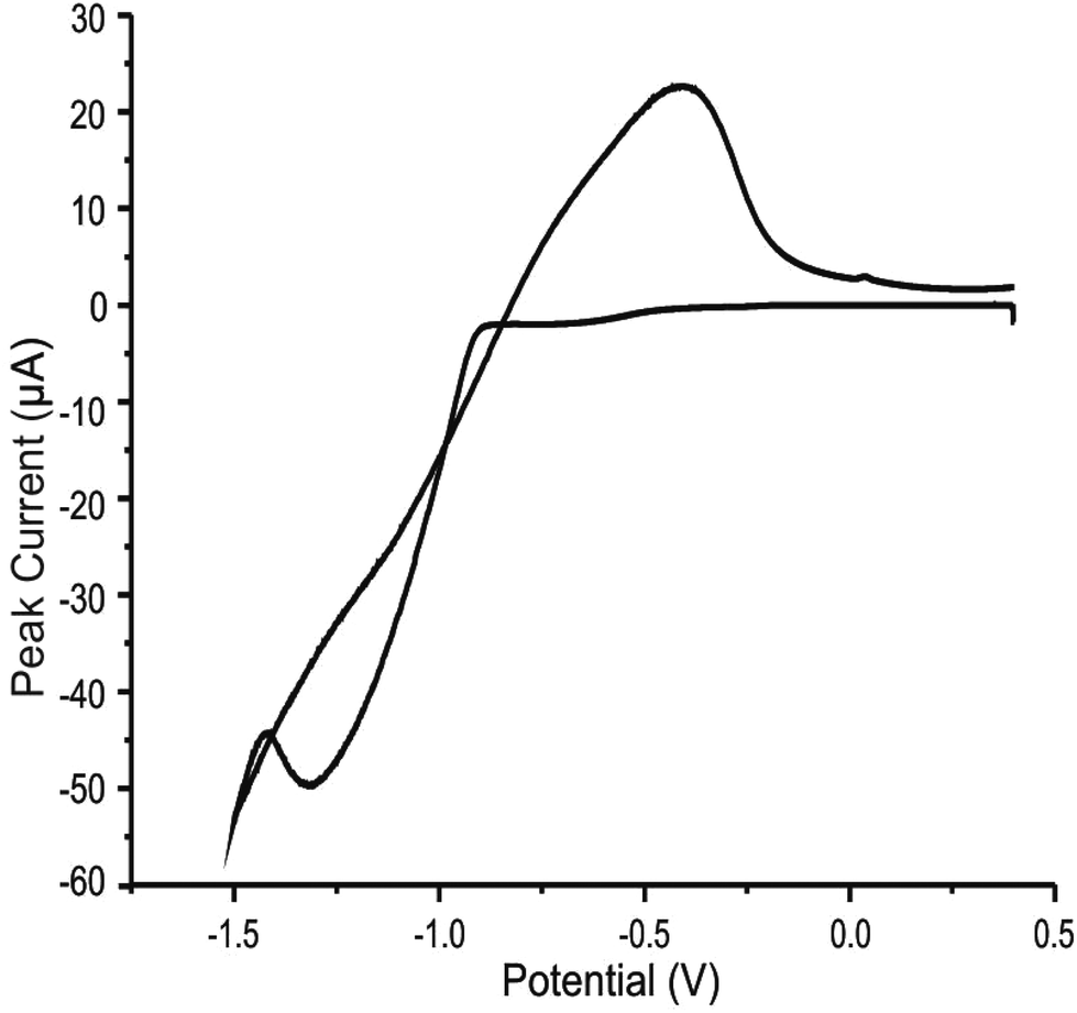 | ||
| Fig. 1 Typical cyclic voltammogram recorded in 1 mM Na2MoO4 (with 1 M NaCl and 1 M NH4Cl, adjusted to pH 8.5), showing the disposition and stripping of MoO2 at an ESPE. Scan rate: 5 mV s−1 (vs. SCE). | ||
Based upon analysis of the typical cyclic voltammogram reported above (Fig. 1), further optimisation (data not shown), and in line with previous literature reports, subsequent electrodeposition of MoO2 nanowires onto our SPEs was achieved using chronoamperometry; performed at either −0.78 (onset of deposition) or −0.92 V (fully initiated deposition) for specific durations.14,30,32,33 Following the establishment of a suitable potential for electrodeposition via chronoamperometry, it was necessary to vary the duration that electrodeposition was performed. In previous work the mean thickness of nanowire deposition was shown to be dependent on the deposition time, thus allowing wires with controlled diameters to be prepared.35 In this work, utilising a range of deposition times (at the above optimised potentials) and performing detailed interpretation with SEM and cyclic voltammetry allowed us to determine deposition times that corresponded to a range of nanowire coverages. As such, deposition times of 256, 384, 512 and 640 seconds were implemented within this work and encompass varied nanowire coverages, from partial to complete electrode coverages. Investigations utilising the range of deposition potentials and times determined above will allow us to observe the effects of the resultant variations in coating/coverage of the SPE surface and the implications of this towards subsequent voltammetry (electron transfer kinetics); thus, the corresponding SEMs and voltammetry are presented later. Note that for the purpose of nanowire fabrication and analysis, immediately after deposition, the respective electrode was removed from the coating solution and any excess solution remaining on the surface was gently removed (rinsed off) with deionised water prior to further testing.
Physicochemical characterisation of MoO2 coated SPEs (edge sites)
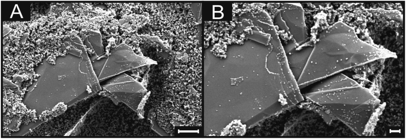
Fig. 2(B) and (C) show SEM images of a typical graphite/graphene flake found in both ESPEs and GSPEs. As is readily observed in Fig. 2(B), the basal plane is several μm in diameter, whereas the thickness of the graphitic sheet (the exposed edge plane sites) observed in Fig. 2(C) is ca. 100–200 nm. Following the coating procedure detailed above, MoO2 nanowires were electrodeposited onto the surface of an ESPE utilising a chronoamperometric procedure lasting 256 seconds at a deposition potential of −0.92 V (corresponding to fully initiated deposition). The SEM images in Fig. 2(E) and (F) were recorded immediately after MoO2 deposition and are distinct from those obtained prior to the process, where now an ensemble of nanowires ca. 100–200 nm in diameter is evident. As detailed earlier, the average thickness of such nanowires has been shown to depend on the deposition time and potential utilised.35 As such, deposition resulting from a potential of −0.78 V (again for 256 seconds) was performed and the resultant SEM images are depicted in Fig. 3. Upon comparison of Fig. 2(E) and 3, it is evident that relatively ‘thin’ (length: ca. 3 μm, width: ca. 50 nm) MoO2 nucleation has occurred on the edge plane sites of the SPEs (comprising graphite flakes) when utilising a potential of −0.78 V. Conversely, using the greater potential of −0.92 V resulted in a ‘thick’ nucleation (length: ca. 3 μm, width: ca. 200 nm) of the MoO2 nanowires occurring.30 Generally, the shortness and uniform morphology of the electrodeposited MoO2 nanowires can be attributed to the amorphous nature of the morphological features comprising the graphite flakes found within the ink of our SPEs. | ||
| Fig. 2 Cyclic voltammetric response towards 1 mM [Ru(NH3)6]3+/2+ in 0.1 M KCl at a bare/unmodified ESPE (A) and using an ESPE following MoO2 deposition (D). Scan rate: 100 mV s−1 (vs. SCE). Note that MoO2 deposition in D was achieved via chronoamperometry at −0.92 V for 256 seconds in 1 mM Na2MoO4, 1 M NaCl, 1 M NH4Cl (adjusted to pH 8.5). SEM images of a bare/unmodified graphite flake (with an observable edge plane site exposed) found upon the surface of an ESPE (B and C) and of a graphitic flake found upon the surface of an MoO2 electrodeposited ESPE (E and F). Scale bars: 1 μm in B and E, and 200 nm in C and F respectively. SEM magnifications were ×30k and ×150k magnification respectively for the progressive images. | ||
 | ||
| Fig. 3 SEM images of a graphitic island comprising an ESPE following being coated (using a pH 8.5 coating solution of 1 mM Na2MoO4, 1 M NaCl and 1 M NH4Cl) at −0.78 V for 256 seconds. Images show MoO2 deposition on the edge plane sites. (A) ×30k magnification (scale bar: 1 μm), (B) ×50k magnification (scale bar: 200 nm). | ||
The two experiments performed above confirm that the MoO2 nanowires are indeed electrodeposited onto edge plane like-sites/defects, with the experiment at the lower deposition potential (−0.78 V) producing incomplete/discontinuous nanowires. Through observation of the incomplete/discontinuous nanowires, it is possible to see the edge plane sites/steps of the graphitic structure emerging from the ends and from beneath the said nanowires. This provides conclusive evidence for the production of MoO2 nanowires using ESPEs and GSPEs as the underlying substrates. Of note is the clear selectivity for the graphitic edge plane (rather than basal plane) sites for MoO2 deposition, which concurs well with previous studies and indicates that ‘edge planes sites are the predominant structures contributing to HET’ occurring on a graphitic electrode's surface (see later for further investigations).12,14,31,58 However, note that further increasing the electrodeposition potential and/or time results in a decreased selectively of nucleation. Fig. 4 depicts the surface of an ESPE following the attempted nanowire deposition utilising a chronoamperometric procedure lasting 640 seconds at a deposition potential of −0.92 V. Electrodeposition for time periods less than 640 seconds can lead to incomplete coverage and the exposure of graphitic sites, such as that seen in ESI Fig. 1.† The resultant ‘thick’ electrodeposited ‘film’ has encompassed and engulfed the entire electrode surface, evidently expanding out from the edge plane like-sites/defects. It is evident that throughout the process, the basal plane sites of the graphene/graphite SPEs remain relatively uncovered, except when the available edge plane sites have been utilised, in which case the MoO2 deposition expands and grows from the ‘reactive’ edge sites, covering the entire surface of the electrode.12,54,58
 | ||
| Fig. 4 Cyclic voltammetric response (A) towards 1 mM [Ru(NH3)6]3+/2+ in 0.1 M KCl utilising an ESPE following MoO2 deposition via chronoamperometry at −0.92 V for 640 seconds in 1 mM Na2MoO4, 1 M NaCl, 1 M NH4Cl; adjusted to pH 8.5. Scan rate: 100 mV s−1 (vs. SCE). Corresponding SEM images showing complete MoO2 deposition/coverage of the ESPE surface at ×10k magnification (B, scale bar: 1 μm) and ×30k magnification (C, scale bar: 1 μm). | ||
Independent physicochemical characterisation was next performed in order to determine the composition of the nucleated materials to unambiguously confirm the presence of the proposed electrodeposited MoO2 nanowires. First, Raman spectroscopy and Raman mapping were performed on both an unmodified ESPE and an ESPE following the electrodeposition process utilising a deposition potential of −0.92 V for 256 seconds. ESI Fig. 2† depicts the resultant Raman spectra of the aforementioned unmodified ESPE (red) and electrodeposited ESPE (black). The Raman spectra of the unmodified ESPE is as expected and as previously reported,37,52 exhibiting a peak at ca. 1580 cm−1 (G band), which is typical of graphitic materials.52,54,59 Accompanying the G band is a peak at ca. 1355 cm−1 (D band), which is characteristic of graphitic defects typically observed in commercially available graphite samples and in SPEs.37,54 Finally, the presence of a small peak (relative to the peak height of the G band) at ca. 2700 cm−1 (2D band) is also characteristic of graphitic materials,54,59 thus confirming the high quality graphitic constituents of the SPEs utilised. Notably, in the spectra of the unmodified ESPE, there are no visible Raman peaks in the region of 100–1000 cm−1. Conversely, when analysing the Raman spectra recorded at the ESPE that has undergone our electrodeposition process (see ESI Fig. 2†), in addition to the characteristic graphitic peaks detailed above, characteristic peaks associated with MoO2 are evident between ca. 100 to 1000 cm−1.60 Notably, individual peaks at ca. 200, 363 and 871 cm−1 are present,60 indicating that the electrodeposited nanowires(material) are(is) indeed comprised of molybdenum oxides and the intended MoO2.
To further support the SEM analysis depicted previously, Raman mapping was also performed in order to offer insight into how/where the electrodeposited MoO2 nanowires form. Raman maps of the aforementioned electrodes were recorded at the Raman intensity of 871 cm−1, which is indicative of MoO2 (as determined above).60 ESI Fig. 3(A) and (B)† shows an optical image and 400 point Raman map of a blank/unmodified ESPE. Although a graphitic flake is visible in the optical image presented, the Raman map depicts a featureless area. There is no indication of MoO2 present and importantly there is no variation in the Raman intensities recorded at 871 cm−1 when the map intercepts the various morphological features of the underlying SPE (i.e. there is no change/difference recorded at the contrasting edge and basal plane sites). ESI Fig. 3(C) and (D)† depict the respective optical image and 400 point Raman map of an ESPE following the electrodeposition process, giving rise to MoO2 nanowire formation (chronoamperometry for 256 seconds at −0.92 V). Close inspection of ESI Fig. 3(D)† clearly shows that the nucleation of MoO2 has occurred onto the SPE surface, as indicated by ‘dark’ patches/areas that seem to follow distinctive patterns. Upon comparing the optical image in ESI Fig. 3(C)† indicating the respective area utilised for the Raman map, it is evident that the MoO2 nanowire electrodeposition appears to occur at the edge planes of the graphite flake visible. Further indicating the presence and formation of MoO2 nanowires on the surface of our SPEs, but more importantly, occurring specifically at the edge plane like-sites/defects comprising the graphitic material.
Last, ESI Fig. 4† depicts an SEM image of a GSPE (following the electrodeposition process noted above at −0.92 V for 384 seconds) with complimentary EDS mapping analysis. EDS mapping was performed to offer insight into the elemental composition of the electrode surface over the electrodeposited area shown. Analysis of the EDS map depicts the coverage of Mo and O on the surface of the ESPE with an atomic percentage of 12.1% and 21.7% respectively. The respective ratio is 1.0![[thin space (1/6-em)]](https://www.rsc.org/images/entities/char_2009.gif) :1.8 for Mo:O. This composition correlates with expected values for the structure of MoO2 (ca. 1.0:2.0 for Mo:O respectively), supporting the former analysis performed and indicating the successful electrodeposition of MoO2 onto the surface of the SPEs.
:1.8 for Mo:O. This composition correlates with expected values for the structure of MoO2 (ca. 1.0:2.0 for Mo:O respectively), supporting the former analysis performed and indicating the successful electrodeposition of MoO2 onto the surface of the SPEs.
Physicochemical characterisation has confirmed the composition and presence of MoO2 nanowires/films, generated via the electrodeposition process indicated. We have demonstrated a procedure allowing the production of variable/tailored MoO2 nanowires onto the surface of SPEs (more specifically, originating at the edge plane like-sites/defects present). Our cheap, versatile and tailored/bespoke SPEs (ESPEs and GSPEs) can be utilised (and the deposition process manipulated) in order to produce nanowires of varying morphologies. The reported simple, scalable and cost effective formation of unique and intriguing MoO2 nanowires and films realised herein (utilising graphite and graphene SPEs) is of significant interest for use in both academic and commercial applications.
Electrochemical characterisation/implications
Having developed the method to selectively electrodeposit and fabricate MoO2 nanowires onto the edge plane like-sites/defects of our SPEs (effectively covering/blocking/inhibiting them), we next explore the resultant electrochemical implications. The distinctive patterns alone, observed in the electrochemical process of nanowire decoration, show that electron transfer occurs predominantly on edge plane sites when utilising SPEs fabricated/comprised of graphitic materials. However, by altering the amount of MoO2 deposition and varying the degree to which said edge plane sites are covered/blocked, we turn our attention towards identifying the role of the edge plane like-sites/defects on the observed voltammetry and monitor the HET performance of our SPEs when correlated to varied ‘blockage’ and MoO2 coverage.
Fig. 2(A) depicts a typical cyclic voltammogram of 1 mM [Ru(NH3)6]3+/2+ (0.1 M KCl) obtained utilising an unmodified ESPE. Inspection of Fig. 2(A) reveals a reduction peak at ca. −0.27 V and an oxidation peak at ca. −0.12 V, resulting in a peak-to-peak separation (ΔEP) of 0.15 V (at 100 mV s−1), which agrees well with the literature.36,37Fig. 2(D) illustrates a comparable cyclic voltammogram obtained at a MoO2 coated ESPE (following an electrodeposition process at −0.92 V for 256 seconds, as detailed above). Interestingly, the voltammetry of [Ru(NH3)6]3+/2+ at the MoO2 coated ESPE exhibits a reduction peak at ca. −0.32 V and an oxidation peak at ca. −0.09 V, resulting in a ΔEP of 0.23 V. As observed, the ESPE with MoO2 nanowires instead of edge plane like-sites/defects (where these sites have been coated/blocked) gives a response with a larger ΔEP than that of the unmodified ESPE. This indicates slower electrode kinetics (HET) in the former case and agrees with the hypothesis that edge plane sites are the predominant origin of electron transfer at graphitic materials,13,14,54 in which the SPE's (comprised of graphite and graphene, see later) response is thus similar to that of HOPG, that is, of a nano-band array.29 The ΔEP and resultant HET rates, k°, of such a random array of nano-bands comprising edge plane sites will depend on the surface coverage, Θ, and respective electron transfer rate constant,  , in which
  is the HET rate constant of the nano-band material. Therefore, above, the ‘reactive’ edge plane sites are blocked/coated with MoO2, resulting in a lower global coverage,
  , and thus an overall decrease in the observed HET rates. Notably, although MoO2 is electrically conductive (i.e. it is not completely insulating), it is a poor electron transfer material.13,14 As such, one might certainly expect a MoO2 electrode to exhibit slower electrode kinetics than (for example) that of a noble metal and of the HET exhibited by the edge plane like-sites/defects of HOPG.13,14 Consequently, as
  is expected to be greater than
  , the increased ΔEP resulting from covering and effectively blocking the edge plane like-sites/defects (reducing the
  ) of our SPEs is easily explained. Of course, if the uncovered (and unaffected) basal plane sites of the graphitic material were the primary reactive sites, then we would expect to observe no changes in the voltammetry. This fact, that we perceive a blocking as a result of reduced HET rates, indicated by a larger ΔEP, when inhibiting the electrochemical reactivity of the edge planes, proves that the edge plane like-sites/defects are the predominant origin of electron transfer at graphitic SPEs. Indeed, the electrochemical reactivity, k°, of the edge and basal planes comprising HOPG have previously been reported as ca. 0.022 and less than 10−9 cm s−1 respectively,29 which (as indicated above) allows one to infer that the basal planes are ‘effectively/comparably’ inert. Although we are considering the presence and reactivity of ‘edge sites’ and ‘basal sites’, note that a range of different ‘defect sites’ will likely be present, which act as further ‘edge sites’ in terms of their reactivity and as such, if they are not blocked/covered, will allow electron transfer akin to that of the edge planes.11,13
We next explore the HET rate constants, k°, of the unmodified and MoO2 coated ESPEs in order to gain further insights. Note that the electrochemical performance/properties of our ESPEs and GSPEs are benchmarked throughout this work utilising k° calculations towards the commonly employed redox probe, [Ru(NH3)6]3+/2+ (1 mM, in 0.1 M KCl), as detailed in the Experimental section and as utilised above. Considering the electrodes above (and as depicted in Fig. 2), that is, an unmodified ESPE and a MoO2 coated ESPE (electrodeposition at −0.92 V for 256 seconds), the corresponding k° values were estimated respectively at ca. 1.56 × 10⁻³ (bare/unmodified ESPE) and 7.02 × 10⁻⁴ cm s−1 (MoO2 coated ESPE). Comparison of the k° values at the unmodified and nanowire coated ESPE clearly indicates a reduction in the electrochemical reactivity of the SPE when the edge plane sites are effectively blocked/coated with MoO2. This further supports the aforementioned crucial insights into the electrochemical properties of these SPEs and indicates that electron transfer occurs predominantly on the edge plane like-sites/defects present on carbon/graphitic-based electrodes.
To observe the effects of varied MoO2 coverage/coating (and resulting variations in the  ) at the graphene-like and graphite SPEs (GSPEs and ESPEs respectively), we next utilised a range of deposition times and potentials in our chronoamperometric process and considered the electrochemical implications of these towards the subsequent voltammetry. The resultant data, including respective ΔEP and k° values, is presented in Table 1. Inspection of Table 1 reveals a correlation/trend, indicating that (when utilising both SPE types) an increase in MoO2 nanowire deposition/coverage (i.e. when increasing the deposition time and/or potential utilised, as described earlier, corresponding to a decreased coverage/availability of edge plane like-sites/defects (i.e. a smaller
  )), results in larger ΔEP and reduced k° values. Interested readers are directed to ESI Fig. 7,† which depicts SEMs of an ESPE surface after undergoing electrodeposition for various durations, highlighting the above inferences. With respect to the earlier optimisation and physicochemical characterisation, given that the electrodeposited MoO2 nanowires ‘reside on’ and ‘effectively block’ the edge plane like-sites/defects of our SPEs, the observed decrease in HET kinetics (apparent when increasing nanowire coverage and decreasing
  ) is further evidence that the origin of electron transfer can be attributed to these ‘active’ edge plane sites at graphitic materials.
| Time (s) | SPE type | Potential (−0.78 V) | Potential (−0.92 V) | ||
|---|---|---|---|---|---|
| k° (cm s−1) | ΔEP (V) | k° (cm s−1) | ΔEP (V) | ||
| NP; it was not possible to determine a value due to the lack of visible redox peaks (i.e. a completely blocked electrode surface resulted, with limited electron transfer occurring). | |||||
| 256 | Graphite (ESPE) | 1.42 × 10⁻³ | 0.17 | 7.02 × 10⁻⁴ | 0.23 |
| 384 | Graphite (ESPE) | 1.18 × 10⁻³ | 0.19 | NP | NP |
| 512 | Graphite (ESPE) | 7.04 × 10⁻⁴ | 0.21 | NP | NP |
| 640 | Graphite (ESPE) | 6.74 × 10⁻⁴ | 0.25 | NP | NP |
| 256 | Graphene (GSPE) | 1.25 × 10⁻³ | 0.18 | 7.92 × 10⁻⁴ | 0.22 |
| 384 | Graphene (GSPE) | 8.18 × 10⁻⁴ | 0.20 | NP | NP |
| 512 | Graphene (GSPE) | 7.99 × 10⁻⁴ | 0.21 | NP | NP |
| 640 | Graphene (GSPE) | 7.87 × 10⁻⁴ | 0.23 | NP | NP |
It is interesting to note that in some instances of high MoO2 coverage, it was not possible to determine the electrochemical values of ΔEP and k°. Such occurrences were due either to the absence of visible redox peaks or the complete lack of observable voltammetry at the given electrodeposited/coated SPE (i.e. in the case of completely covering/blocking the electrode surface with MoO2, this resulted in limited underlying electron transfer occurring). It is apparent from Table 1 that greater MoO2 electrodeposition (lower  ) results in reduced HET rates. This correlation continues until a complete blocking of the underlying electron transfer processes occurs. In such cases (as evidenced in Fig. 4), the coverage of MoO2 corresponds to that described earlier, where all of the available edge plane sites are exhausted/covered and resultantly, MoO2 deposition expands outwards from the nucleated edge sites, covering/engulfing and blocking the entire surface of the electrode via creating a thick film. Fig. 4 shows the accompanying SEMs that are typical of this stage of coverage, in which an ESPE underwent MoO2 electrodeposition at −0.92 V for 640 seconds. Fig. 4 also shows the resultant cyclic voltammetric response towards [Ru(NH3)6]3+/2+ (1 mM, in 0.1 M KCl), where the absence of visible redox peaks is apparent. The gradual inhibition of the SPE's HET rates corresponding to a decreased
  (and increased MoO2 nanowire coverage) until a complete blocking of the underlying electron transfer reactivity/ability is achieved, further confirms the inferences of this work. The distinct electron transfer properties of edge and basal plane sites on graphitic materials are clearly presented and indicate favourable/greater electrochemical reactivity at the edge planes in contrast to limited reactivity at the basal plane sites.
Although the results/trends reported in this paper are observed at both the ESPEs and GSPEs (see Table 1) it is noted that upon the initial deposition of MoO2 nanowires onto the GSPE (and results obtained thereafter) an increased k° value is observed. Indeed, the k° value (and resultant electrochemical HET performance) of the unmodified GSPE remains ‘less’ than that of the nanowire modified GSPEs throughout. Given that, by its nature, the GSPE (i.e. graphene) has a lower global coverage of edge plane  than that of the ESPE (i.e. graphite) and resultantly has a large geometric contribution of basal plane comprising its structure, it is likely that the respective HET rates, k°, of the materials (that is,
  , as inferred previously),12,13,54 result in the modified MoO2 layer being ‘more electrochemically reactive/favourable’ in the case of single-layer graphene's basal plane (and that of the GSPE), resulting in the observed occurrence. Further, it may be likely that in blocking/coating graphene's single edge plane band with MoO2, favourable changes in the mass transport mechanism present occur (with respect to improving [Ru(NH3)6]3+/2+ transport to/from the basal planes) and result in improvements to the observed voltammetry.11,13 Whatever the cause, this is a fascinating observation that will require further (more in-depth and separate) examination. Another consideration is the noticeable capacitance (capacitive current) observed when performing electrochemistry with the MoO2 nanowires electrodeposited on the SPE's surface. The observed capacitance increases proportionally as one effectively blocks the reactive surface of the electrode with additional MoO2 and resultantly this effect continues (increasing) until the entire electrode surface is blocked/coated with MoO2 (corresponding to the ‘thick film’ formation as noted above), in which case there are no observable redox peaks for the electrochemical processes studied herein (only a capacitive current). This is as expected when one effectively passivates an underlying electrode and may have interesting academic/industrial implications for various applications.
A further interesting point to consider is the effect that nanowire fabrication imparts upon the magnitude of the peak currents observed. It has previously been reported that a change in electrode kinetics from that of a ‘fully reversible electron transfer process’ to the case of a ‘fully irreversible process’ will give rise to a marginal decrease in the voltammetric peak current, which, as governed by the Randles–Ševćik equation, is attributed to the reversible/irreversible limits differing by a factor of 1.27.21 Thus in our case, if we take an ESPE, which exhibits reversible electrode kinetics, and modify the surface with MoO2 nanowires so that electron transfer is inhibited (resulting in a modified electrode exhibiting irreversible electrode kinetics), a reduction in the magnitude of the peak current should be observed by a factor of 1.27. Indeed, we observe only marginal alterations in the peak currents obtained following initial/partial nanowire fabrication and prior to the complete blocking process of the ESPE's surface.21 However, due to the interference caused by the above noted ‘capacitive current’ shielding/distorting the expected voltammetric peaks, we are unable to analyse any further correlations occurring in the deviating peak currents.
Finally, cyclic voltammetry with both unmodified and MoO2 nanowire modified ESPEs was performed towards other redox couples and gave the exact same results as observed above. ESI Fig. 5† depicts the typical cyclic voltammetric responses towards N,N,N′,N′-tetramethyl-p-phenylenediamine (TMPD) in 0.1 M KCl and 1 mM Feaq2+/3+ in 0.2 M HClO4, (Feaq2+/3+ solution was made from Fe(NH4)2-(SO4)2-6H2O and 70% HClO4).61 ESI Fig. 5(A) and (B)† clearly show (in line with previous insights) that selectively blocking the edge plane like-sites/defects (and effectively passivating the entire surface) of our SPEs with MoO2 nanowire arrays following an electrodeposition process at −0.92 V for 640 seconds, in both instances, results in an inhibited and reduced electrochemical performance (where the underlying HET properties have been, essentially, blocked). Thus, the previous inferences are further confirmed/strengthened.
Conclusions
In this work, we have fabricated MoO2 nanowire arrays onto graphene and graphite based SPEs for the first time. We have shown that the electrochemical process of nanowire decoration occurs selectively onto the edge plane like-sites/defects of these graphitic materials. Exploring the cyclic voltammetry and resultant electrochemical properties of unmodified and nanowire electrodeposited SPEs has provided crucial insights towards exposing and answering some fundamental questions. Comparison of the HET rate constants, k°, at unmodified and nanowire coated SPEs shows a reduction in the electrochemical reactivity of SPEs when the edge plane sites are effectively blocked/coated with MoO2. This clearly illustrates the distinct electron transfer properties of edge and basal plane sites on graphitic materials, indicating favourable electrochemical reactivity at the edge planes in contrast to limited reactivity at the basal plane sites. We now know categorically that the edge plane like-sites/defects of our SPEs are responsible for the cyclic voltammetry observed. What, however, are the implications for the basal plane of graphitic materials? In line with previous studies,13,14,19,29,54 the results of our electrodeposition experiments and ‘site knock out’ protocol performed herein demonstrate that the basal plane cannot be completely inert. However, it is inferred that is significantly smaller than
  (otherwise we would have observed completely different voltammetry). Essentially, the edge plane like-sites/defects of graphitic-based electrode materials are shown to be the prominent origin of electron transfer (and the observed voltammetric/electrochemical response, exhibiting anomalously fast electrochemical reactions), where in comparison, the basal plane is effectively inert.13,14,19,29,54 Given that all graphitic electrodes are made of the same fundamental building blocks (that is, graphene sheets), there is no reason why these findings cannot be applied to the other prevalent (or newly emerging) carbon-based electrode materials utilised in the field.
Acknowledgements
D. A. C. Brownson acknowledges funding from the Ramsay Memorial Fellowships Trust and all authors acknowledge a British Council Institutional Link grant (no. 172726574) for the support of this research.Notes and references
- R. L. McCreery, Chem. Rev., 2008, 108, 2646–2687 CrossRef CAS PubMed.
- D. A. C. Brownson and C. E. Banks, Electrochem. Commun., 2011, 13, 111–113 CrossRef CAS.
- M. Lu, K. E. Toghill and R. G. Compton, Electroanalysis, 2011, 23, 1089–1094 CrossRef CAS.
- M. Musameh, J. Wang, A. Merkoci and Y. Lin, Electrochem. Commun., 2002, 4, 743–746 CrossRef CAS.
- A. Koca, Int. J. Hydrogen Energy, 2009, 34, 2107–2112 CrossRef CAS.
- Y. Shen, J. Liu, J. Jiang, B. Liu and S. Dong, J. Phys. Chem. B, 2003, 107, 9744–9748 CrossRef CAS.
- J. Yin, J. B. Jia and L. D. Zhu, Int. J. Hydrogen Energy, 2008, 33, 7444–7447 CrossRef CAS.
- D. A. C. Brownson, P. J. Kelly and C. E. Banks, RSC Adv., 2015, 5, 37281–37286 RSC.
- A. T. Valota, I. A. Kinloch, K. S. Novoselov, C. Casiraghi, A. Eckmann, E. W. Hill and R. A. W. Dryfe, ACS Nano, 2011, 5, 8809–8815 CrossRef CAS PubMed.
- M. A. Edwards, P. Bertoncello and P. R. Unwin, J. Phys. Chem. C, 2009, 113, 9218–9223 CAS.
- D. A. C. Brownson and C. E. Banks, The Handbook of Graphene Electrochemistry, Springer, London, 2014 Search PubMed.
- D. A. C. Brownson, L. J. Munro, D. K. Kampouris and C. E. Banks, RSC Adv., 2011, 1, 978–988 RSC.
- D. A. C. Brownson, D. K. Kampouris and C. E. Banks, Chem. Soc. Rev., 2012, 41, 6944–6976 RSC.
- T. J. Davies, M. E. Hyde and R. G. Compton, Angew. Chem., Int. Ed., 2005, 44, 5121–5126 CrossRef CAS PubMed.
- C. E. Banks, R. R. Moore, T. J. Davies and R. G. Compton, Chem. Commun., 2004, 1804–1805 RSC.
- C. E. Banks, T. J. Davies, G. G. Wildgoose and R. G. Compton, Chem. Commun., 2005, 829–841 RSC.
- G. Zhang, P. M. Kirkman, A. N. Patel, A. S. Cuharuc, K. McKelvey and P. R. Unwin, J. Am. Chem. Soc., 2014, 136, 11444–11451 CrossRef CAS PubMed.
- A. N. Patel, M. G. Collignon, M. A. O'Connell, W. O. Y. Hung, K. McKelvey, J. V. Macpherson and P. R. Unwin, J. Am. Chem. Soc., 2012, 134, 20117–20130 CrossRef CAS PubMed.
- S. C. S. Lai, A. N. Patel, K. McKelvey and P. R. Unwin, Angew. Chem., Int. Ed., 2012, 51, 5405–5408 CrossRef CAS PubMed.
- C. G. Williams, M. A. Edwards, A. L. Colley, J. V. Macpherson and P. R. Unwin, Anal. Chem., 2009, 81, 2486–2495 CrossRef CAS PubMed.
- D. A. C. Brownson, C. W. Foster and C. E. Banks, Analyst, 2012, 137, 1815–1823 RSC.
- K. K. Cline, M. T. McDermott and R. L. McCreery, J. Phys. Chem., 1994, 98, 5314–5319 CrossRef CAS.
- K. R. Kneten and R. L. McCreery, Anal. Chem., 1992, 64, 2518–2524 CrossRef CAS.
- H. Chang and A. J. Bard, Langmuir, 1991, 7, 1143–1153 CrossRef CAS.
- C. E. Banks and R. G. Compton, Analyst, 2006, 131, 15–21 RSC.
- D. A. C. Brownson, M. Gomez-Mingot and C. E. Banks, Phys. Chem. Chem. Phys., 2011, 13, 20284–20288 RSC.
- D. A. C. Brownson, R. V. Gorbachev, S. J. Haigh and C. E. Banks, Analyst, 2012, 137, 833–839 RSC.
- L. C. S. Figueiredo-Filho, D. A. C. Brownson, O. Fatibello-Filho and C. E. Banks, Analyst, 2013, 138, 4436–4442 RSC.
- T. J. Davies, R. R. Moore, C. E. Banks and R. G. Compton, J. Electroanal. Chem., 2004, 574, 123–152 CrossRef CAS.
- E. C. Walter, M. P. Zach, F. Favier, B. J. Murray, K. Inazu, J. C. Hemminger and R. M. Penner, ChemPhysChem, 2003, 4, 131–138 CrossRef CAS PubMed.
- M. E. Hyde, T. J. Davies and R. G. Compton, Angew. Chem., Int. Ed., 2005, 44, 6491–6496 CrossRef CAS PubMed.
- M. P. Zach, K. H. Ng and R. M. Penner, Science, 2000, 290, 2120–2123 CrossRef CAS PubMed.
- M. P. Zach, K. Inazu, K. H. Ng, J. C. Hemminger and R. M. Penner, Chem. Mater., 2002, 14, 3206–3216 CrossRef CAS.
- X. Ji, C. E. Banks, W. Xi, S. J. Wilkins and R. G. Compton, J. Phys. Chem. B, 2006, 110, 22306–22309 CrossRef CAS PubMed.
- M. E. Hyde, T. J. Davies and R. G. Compton, Angew. Chem., 2005, 117, 6649–6654 CrossRef.
- C. W. Foster, J. P. Metters and C. E. Banks, Electroanalysis, 2013, 25, 2275–2282 CAS.
- E. P. Randviir, D. A. C. Brownson, J. P. Metters, R. O. Kadara and C. E. Banks, Phys. Chem. Chem. Phys., 2014, 16, 4598–4611 RSC.
- E. Blanco, C. W. Foster, L. R. Cumba, D. R. D. Carmo and C. E. Banks, Analyst, 2016, 141, 2783–2790 RSC.
- F. Wantz, C. E. Banks and R. G. Compton, Electroanalysis, 2005, 17, 655–661 CrossRef CAS.
- C. Burda, X. Chen, R. Narayanan and M. A. El-Sayed, Chem. Rev., 2005, 105, 1025–1102 CrossRef CAS PubMed.
- J. Karthikeyan, V. Kumar and P. Murugan, J. Phys. Chem. C, 2015, 119, 13979–13985 CAS.
- X. Yao, X. Zhang and J. Wang, Int. J. Quantum Chem., 2015, 115, 607–617 CrossRef CAS.
- A. Kobler, T. Beuth, T. Klöffel, R. Prang, M. Moosmann, T. Scherer, S. Walheim, H. Hahn, C. Kübel, B. Meyer, T. Schimmel and E. Bitzek, Acta Mater., 2015, 92, 299–308 CrossRef CAS.
- S. H. Shen, I. S. Wang, H. Cheng and C. T. Lin, Sens. Actuators, B, 2015, 218, 303–309 CrossRef CAS.
- Q. Wan, Q. H. Li, Y. J. Chen, T. H. Wang, X. L. He, J. P. Li and C. L. Lin, Appl. Phys. Lett., 2004, 84, 3654–3656 CrossRef CAS.
- M. S. Gudiksen, L. J. Lauhon, J. Wang, D. C. Smith and C. M. Lieber, Nature, 2002, 415, 617–620 CrossRef CAS PubMed.
- Y. Li, F. Qian, J. Xiang and C. M. Lieber, Mater. Today, 2006, 9, 18–27 CrossRef CAS.
- C. W. Foster, R. O. Kadara and C. E. Banks, Screen-Printing Electrochemical Architectures, Springer, London, 2016 Search PubMed.
- A. B. Laursen, A. S. Varela, F. Dionigi, H. Fanchiu, C. Miller, O. L. Trinhammer, J. Rossmeisl and S. Dahl, J. Chem. Educ., 2012, 89, 1595–1599 CrossRef CAS.
- S. J. Rowley-Neale, D. A. C. Brownson, G. C. Smith, D. A. G. Sawtell, P. J. Kelly and C. E. Banks, Nanoscale, 2015, 7, 18152–18168 RSC.
- N. A. Choudry, D. K. Kampouris, R. O. Kadara and C. E. Banks, Electrochem. Commun., 2010, 12, 6–9 CrossRef CAS.
- L. R. Cumba, J. P. Smith, D. A. C. Brownson, J. Iniesta, J. P. Metters, D. R. D. Carmo and C. E. Banks, Analyst, 2015, 140, 1543–1550 RSC.
- L. C. S. Figueiredo-Filho, D. A. C. Brownson, M. Gomez-Mingot, J. Iniesta, O. Fatibello-Filho and C. E. Banks, Analyst, 2013, 138, 6354–6364 RSC.
- D. A. C. Brownson, S. A. Varey, F. Hussain, S. J. Haigh and C. E. Banks, Nanoscale, 2013, 6, 1607–1621 RSC.
- D. A. C. Brownson, A. C. Lacombe, M. Gomez-Mingot and C. E. Banks, RSC Adv., 2012, 2, 665–668 RSC.
- D. A. C. Brownson, L. C. S. Figueiredo-Filho, B. L. Riehl, B. D. Riehl, M. Gomez-Mingot, J. Iniesta, O. Fatibello-Filho and C. E. Banks, J. Mater. Chem. A, 2016, 4, 2617–2629 CAS.
- R. S. Nicholson, Anal. Chem., 1965, 37, 1351–1355 CrossRef CAS.
- D. A. C. Brownson, A. C. Lacombe, D. K. Kampouris and C. E. Banks, Analyst, 2012, 137, 420–423 RSC.
- A. C. Ferrari, Solid State Commun., 2007, 143, 47–57 CrossRef CAS.
- G. Solferino and A. J. Anderson, Chem. Geol., 2012, 322–323, 215–222 CrossRef CAS.
- P. Chen and R. L. McCreery, Anal. Chem., 1996, 68, 3958–3965 CrossRef CAS.
Footnote |
| † Electronic supplementary information (ESI) available. See DOI: 10.1039/c6nr04220a |
| This journal is © The Royal Society of Chemistry 2016 |