
 Open Access Article
 This Open Access Article is licensed under a
 Creative Commons Attribution 3.0 Unported Licence
Finite-size scaling in silver nanowire films: design considerations for practical devices†
Matthew J.
Large
 *ab,
Maria
Cann
c,
Sean P.
Ogilvie
b,
Alice A. K.
King
b,
Izabela
Jurewicz
a and
Alan B.
Dalton
*b
*ab,
Maria
Cann
c,
Sean P.
Ogilvie
b,
Alice A. K.
King
b,
Izabela
Jurewicz
a and
Alan B.
Dalton
*b
aUniversity of Surrey, Guildford, Surrey GU2 7XH, UK
bUniversity of Sussex, Falmer, East Sussex BN1 9RH, UK. E-mail: m.large@sussex.ac.uk; a.b.dalton@sussex.ac.uk
cM-Solv Ltd, Oxonian Park, Kidlington OX5 1FP, UK
First published on 27th June 2016
Abstract
We report the first application of finite-size scaling theory to nanostructured percolating networks, using silver nanowire (AgNW) films as a model system for experiment and simulation. AgNWs have been shown to be a prime candidate for replacing Indium Tin Oxide (ITO) in applications such as capacitive touch sensing. While their performance as large area films is well-studied, the production of working devices involves patterning of the films to produce isolated electrode structures, which exhibit finite-size scaling when these features are sufficiently small. We demonstrate a generalised method for understanding this behaviour in practical rod percolation systems, such as AgNW films, and study the effect of systematic variation of the length distribution of the percolating material. We derive a design rule for the minimum viable feature size in a device pattern, relating it to parameters which can be derived from a transmittance–sheet resistance data series for the material in question. This understanding has direct implications for the industrial adoption of silver nanowire electrodes in applications where small features are required including single-layer capacitive touch sensors, LCD and OLED display panels.
1. Introduction
Random silver nanowire (AgNW) networks have attracted significant attention in recent years as a potential alternative to Indium Tin Oxide (ITO) in many applications; particularly capacitive touch sensors. Recent market analysis suggests that AgNW films may attract up to a 10% share of the transparent conductor market by 2025, with a total market value of approximately $900 m per year.1 As such, it is critical to understand the behaviour of these materials in the context of real devices.Particulate films behave inherently differently as transparent conductors to continuous material films such as ITO. The most notable and well-studied difference is the presence of a “percolative” region in their transmittance–resistance curves.2–6 This is where the conductivity of the film scales as a power law with the particle density (measured either using the surface fraction4,6 or the film thickness2). This conductivity scaling is well understood in terms of percolation theory.7
The production of working devices from a transparent conductive film involves patterning of the material to produce isolated electrode structures. This can be easily achieved by either lithographic processes or laser ablation.8 For continuous materials like ITO the sensor design can rely on the sheet resistance of the film being constant for different feature sizes. For materials such as AgNW films, however, percolation theory predicts a more complex behaviour termed “finite-size scaling”.7 As feature sizes become progressively smaller, the average sheet resistance of the film varies according to a power law, and there is also an increase in the spatial variability. The prominence of these effects is also a function of the density of the nanowire network. Aspects of this behaviour have previously been experimentally observed.8,9
In this paper we show experimental observations of the finite-size scaling effect in industrially relevant AgNW films patterned by laser ablation, as well as simulation results. By applying established finite-size scaling theory we develop a design rule for small features in nanowire films. This rule relates the minimum feature size that maintains a constant film sheet resistance to the nanowire size distribution and film density. We expect this to have a significant impact on industrial-scale device design employing silver nanowire films as a transparent conductive layer.
2. Methods and materials
2.1 Silver nanowire material
AgNW dispersions were purchased from a commercial supplier and diluted from their as-received state with isopropanol (IPA) to a ratio of 0.75![[thin space (1/6-em)]](https://www.rsc.org/images/entities/char_2009.gif) :10 by weight. The mean length and length standard deviation are measured to be 〈l〉 = 12.4 μm and σl = 4.5 μm respectively (from AFM). The diameters are approximately normally distributed with 〈d〉 = 30 nm and σd = 4 nm.
:10 by weight. The mean length and length standard deviation are measured to be 〈l〉 = 12.4 μm and σl = 4.5 μm respectively (from AFM). The diameters are approximately normally distributed with 〈d〉 = 30 nm and σd = 4 nm.
2.2 Ultrasonic treatment and spray deposition
Ultrasonication of diluted AgNW dispersions was performed using a Fisher Scientific FB15051 ultrasonic bath (∼300 W nominal output power) in swept frequency mode. Spray deposition was performed using a consumer airbrush with a commercial air compressor (Impax IM200-12L). A spraying pressure of 5 bar was used.2.3 AFM characterisation
AFM measurements were performed on an NT-MDT AFM system in semi-contact mode, using cantilevers with a resonant frequency between 200 and 300 kHz. For length distribution measurements, three 100 × 100 μm fields were taken on each sample, and length measurements were made using ImageJ software.102.4 UV-Visible spectroscopy and sheet resistance measurements
UV-Visible spectral measurements were performed using both a Shimadzu UV2501PC dual-beam spectrophotometer and a Camspec M350 dual-beam spectrophotometer. Transmittance measurements for the un-coated substrates were taken for each sample. All transmittance values are measured at 550 nm unless otherwise stated.Sheet resistance for large films is measured in a two-point geometry by applying bar electrodes of silver paint (Agar Scientific G3790) with along-bar resistance of order 1 Ω to opposite ends of the sample. Measurements were made using a Keithley 2400 Sourcemeter. For patterned track structures, silver paint electrodes are also applied and the resistance of the track measured by an ISO-Tech IDM 61 Multimeter.
2.5 Laser processing
AgNW and ITO films are laser ablated using a 1064 nm laser (SPI G4 20 W HS series laser) with an 18 ns pulse duration (FWHM), operating at 100 kHz. The beam is focused through a telecentric F-theta lens and manipulated through a galvanometer scanner (ScanLab). Single shot laser ablation is overlapped through the scanner to produce electrically isolating scribes. The design is defined by a CAD drawing and split up into a number of tiles because of the limited scan field. These tiles are stitched together using step movements of an X–Y sample stage.The CAD design comprises an array of narrow tracks 30, 45, 60, 75 and 100 μm wide with contact pads at either end. The width of the patterned lines varies slightly depending on the film material because of the different ablation threshold fluences of ITO and AgNW films.9
3. Results and discussion
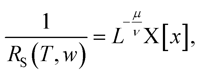
Large area films (of the order of 5 × 10 cm) of AgNWs on glass substrates are patterned by laser ablation to produce a set of “dog bone” track structures which have a conductive region of width w (and length l ≫ w) electrically isolated from the rest of the film material. Fig. 1(A) shows a characteristic optical micrograph of an isolated track structure from this study. The process of laser ablation of nanowire materials is described in detail elsewhere.11 For each value of w tested the average sheet resistance (and standard deviation in the sheet resistance) is measured over 21 samples to investigate the statistical effect of confining percolating nanowire films to narrow geometries. These results are shown in Fig. 1(C) and are compared to electrical percolation simulations of nanowire films in narrow-track geometries.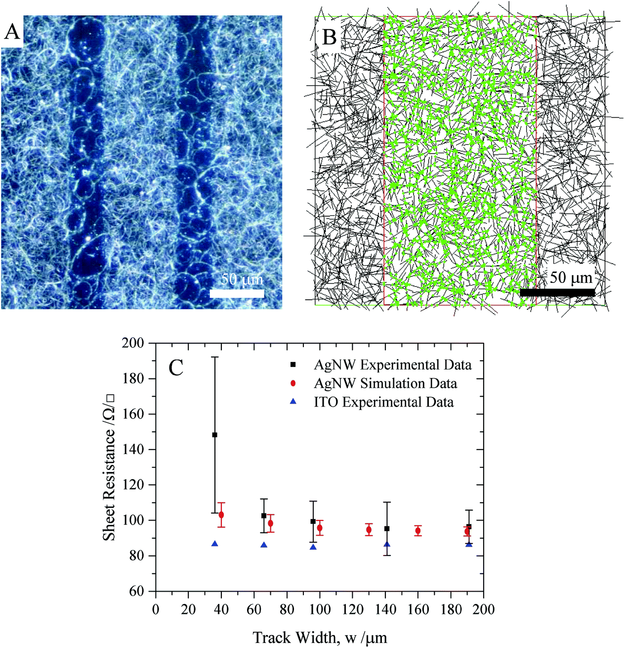 | ||
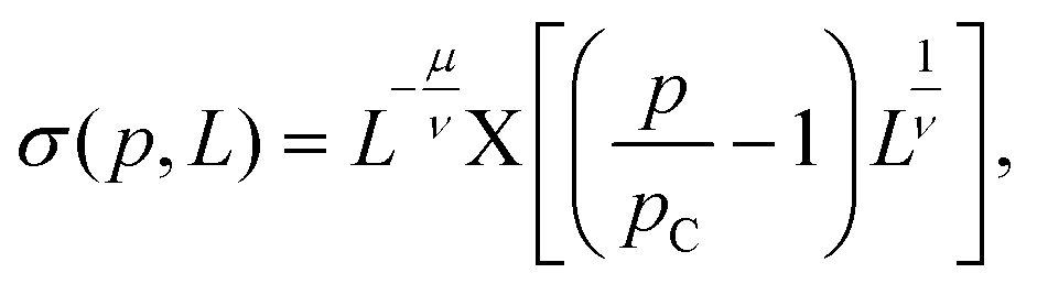
| Fig. 1 (A) Optical micrograph of a laser patterned AgNW film on a glass substrate, with a track structure which is 65 μm wide. (B) Example simulation of a nanowire film; black rods denote nanowires, the red area denotes the “track” region along which the resistance is calculated (between top and bottom edges of the domain), and green dots denote NW-NW junctions. (C) Comparison of measurements and simulations of the film sheet resistance as a function of track width for as-received AgNWs. Data for a comparable commercial ITO film is also shown. Each experimental data point was averaged from 21 individual measurements, with statistical outliers removed (see ESI† for details of the algorithm employed). Each simulation data point is averaged from 50 generations. | ||
The algorithm used in these simulations is a variation on that described by Li and Zhang;12,13 a detailed description is given in the ESI.†Fig. 1(B) gives an example of the model structure. AgNWs (black rods) are distributed isotropically on a square domain, with lengths sampled from the fitted distribution functions shown in Fig. 3(A). Only the sub-region of the AgNW network inside the red box is considered when the sheet resistance is calculated, simulating the narrow track structure; the NW–NW junctions in this area are shown (green dots). Electrical calculations are performed assuming a fixed value for the inter-nanowire junction resistance, and the nanowire resistivity used is that of bulk silver.
According to finite-size scaling (FSS) theory, any variable σ in a percolation problem that scales according to σ = σ0(p − pC)μ, in the infinite domain limit, can be described by;14
 | (1) |
For the case of electrical sheet resistance in real films we can translate eqn (1) to the continuum case;†
 | (2) |
Aspects of the percolation scaling of AgNW films which are relevant to the FSS behaviour can be deduced directly from transmittance–sheet resistance (T–R) measurements. As described elsewhere,15 the authors have developed a T–R model designed to describe the behaviour of rod-like percolating transparent conductor materials (such as metallic nanowires or carbon nanotubes) taking account of their length distribution;
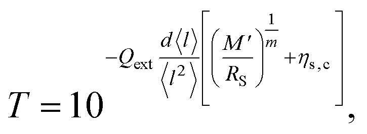
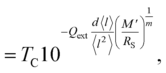
 | (3) |
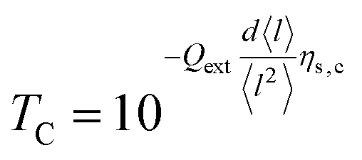
As can be seen in eqn (2) and (3), several parameters relevant to the FSS behaviour can be extracted from the T–R curve of a material by fitting eqn (3) to experimental T–R data; namely the conductivity exponent m and the length distribution parameter 〈l2〉/〈l〉 (and as a result the critical transmittance TC). The critical transmittance is defined in the limit that RS → ∞ in eqn (3), which is the film transmittance at the percolation threshold. The term TC is defined by the microstructural properties of the nanowires (diameter, length distribution statistics), their optical interactions (extinction efficiency) and the universal percolation threshold for rods.
Fig. 2(A) illustrates this T–R fitting on an experimental data series (a.k.a. T–R curve) for as-received AgNW material. Eqn (3) is fitted to the experimental data using 〈l2〉/〈l〉, M′ and m as fitting parameters, where d = (30 ± 4) nm was determined by TEM measurements. The optimised fit values are 〈l2〉/〈l〉 = (13.8 ± 0.2) μm, M′ = (1800 ± 200) Ω □−1 and m = 1.33 ± 0.044, where uncertainties were evaluated using a statistical “delete one” jackknifing procedure.18
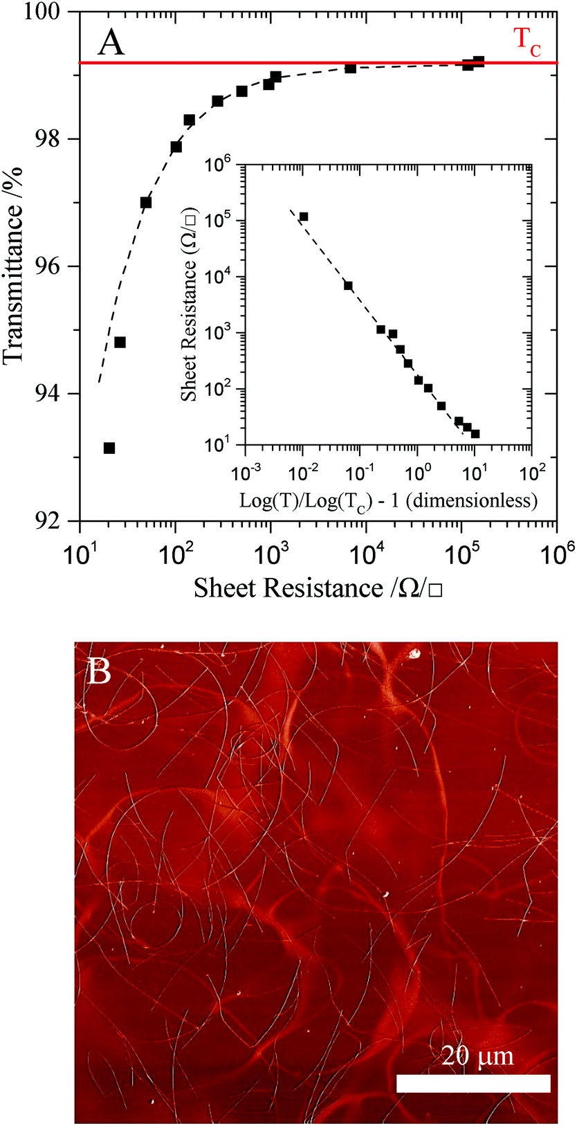 | ||
| Fig. 2 (A) Shows a T–R curve for the as-received AgNW material. The data is fitted in the percolative region using eqn (3). The value of TC resulting from this fit is shown. (Inset) gives a log–log plot of RS against logT/logTc − 1. The bulk and percolative regions can be distinguished by their gradient, with the bulk region having a gradient of −1 and the percolative region having a gradient of −m (where m is the percolative exponent of the sheet resistance). (B) Shows a phase contrast AFM image of a AgNW film with sheet resistance RS ≈ 10 kΩ □−1. | ||
Of particular practical importance is the minimum domain size for which a percolating system behaves as a continuous material. This is directly relevant to device design as we are able to dictate the smallest feature size which can be produced while maintaining a reliable sheet resistance in AgNW films.
This can be understood by plotting ln[σLμ/ν] against ln[x]. As demonstrated by Margolina and Herrmann,19 we find that the data tend to a linear relationship for large values of x (corresponding to large domain sizes and high film densities) and negatively deviate from this trend for lower values (smaller sizes and lower densities). The point at which this deviation becomes significant over many data sets describes the minimum domain size. The trend itself represents the “infinite limit” film behaviour, and can be practically defined in terms of the parameters m and M′ derived from T–R fitting of macroscopic films. In order to account for the fact that the values of m and M′ will vary between different AgNW materials, it is sensible to plot only the deviations of the data from the large-x trend calculated on a data set-wise basis. This can be shown to reduce to ln[RS(T, ∞)/RS(T, w)] (see ESI†).
By defining the value xmin as the point at which nanowire films cease to behave in a two-dimensional fashion, we can deduce an expression for the minimum physical feature size wmin for a given nanowire-based device;
 | (4) |
We see from eqn (4) that wmin is predicted to scale with the parameter 〈l2〉/〈l〉. By mixing nanowire populations with two different length distributions, it is therefore possible to manipulate the minimum feature size to accommodate different device geometries. Fig. 3(A) shows measured length distributions for the as-received AgNW material as well as material processed by ultrasonication for 180 s. Based on the mean and standard deviation of the fitted lognormal distribution we find that 〈l2〉/〈l〉 = (14.0 ± 0.1) μm for the as-received AgNWs (consistent with the value obtained from the T–R fit to the data of Fig. 2(A)).
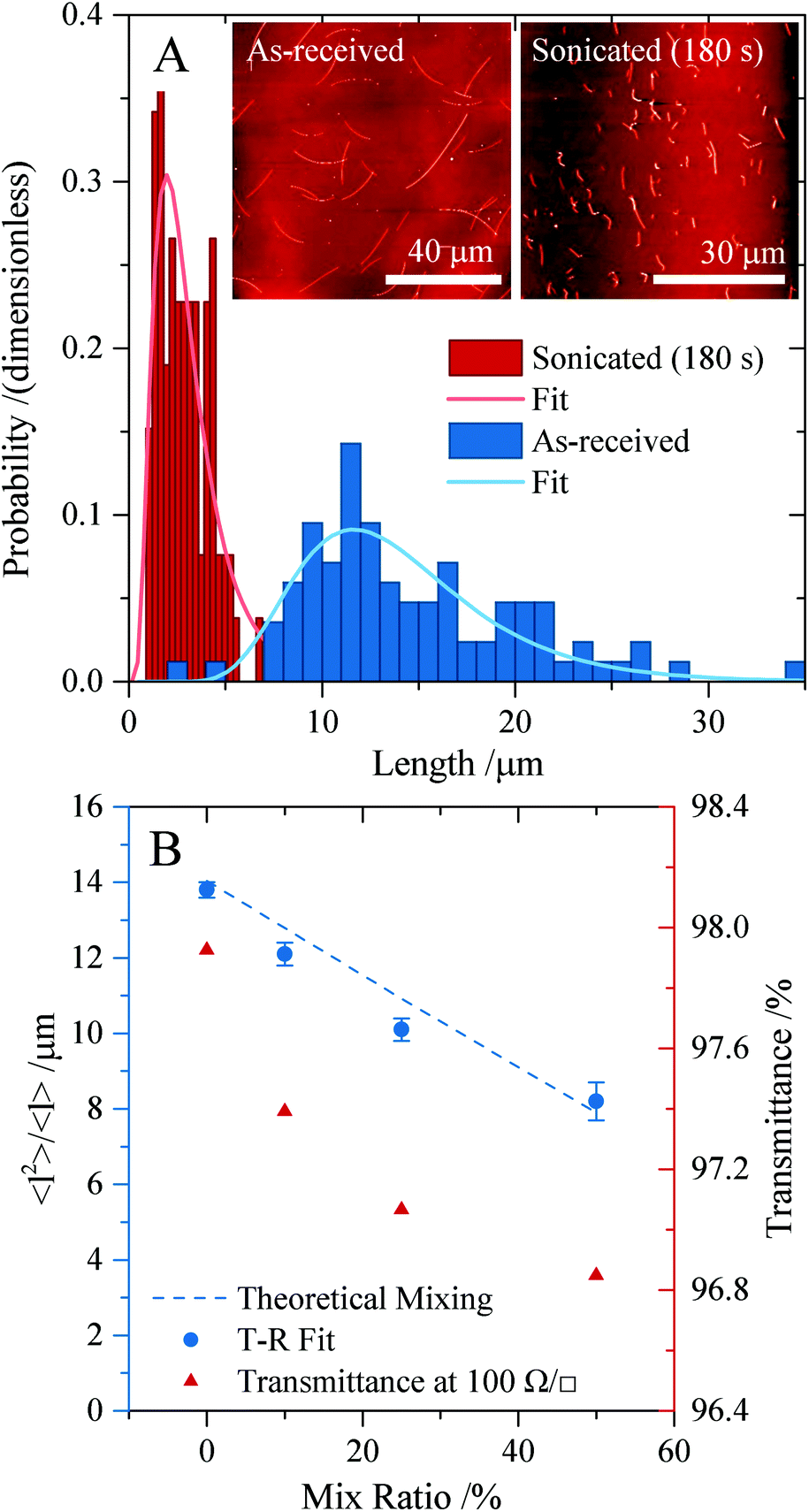 | ||
| Fig. 3 (A) AFM measured length distributions of as-received and sonicated AgNW material. The plot shows length histograms (for N ∼ 100) with fitted lognormal distribution functions. (Inset) characteristic AFM height images used for measurements, showing unsonicated (left) and sonicated (right) samples. (B) Fitted values for the length distribution parameter 〈l2〉/〈l〉 obtained from T–R curves of dispersions prepared by mixing unsonicated and sonicated dispersions with the given volume mixing ratio (left axis). Also shown is the transmittance of the mixed length films at RS = 100 Ω □−1 (right axis). | ||
Fig. 3(B) demonstrates the control of nanowire film properties via simple manipulation of the length distribution. The “long” and “short” nanowires are mixed in solution and T–R curves taken. Measurements of 〈l2〉/〈l〉 are obtained by the same T–R fitting method as shown in Fig. 2(A), and are compared with calculated values derived from the AFM measurements of Fig. 3(A). Also plotted is the approximate transmittance at 100 Ω □−1.
Fig. 4(A) compares plots of ln[RS(T, ∞)/RS(T, w)] against ln[x] for both experiments and simulations, aggregating data taken for each of the mixing ratios of short (sonicated) to long (unsonicated) nanowires shown in Fig. 3(B). The estimated value of xmin is indicated, and agrees well between the experimental and simulation data sets. The data are plotted with five-point moving averages (lines) as well as five-point moving standard deviations (shaded areas). Fig. 4(B) shows a plot of the T–R curve for the 0% mix ratio (as-received AgNW material) alongside the predicted value of wmin from eqn (4) for each value of RS. Fig. 4(C) plots the transmittance of AgNW films at 100 Ω □−1 (from Fig. 3(B)) with the predicted value of wmin as a function of mixing fraction for the volume ratios considered.
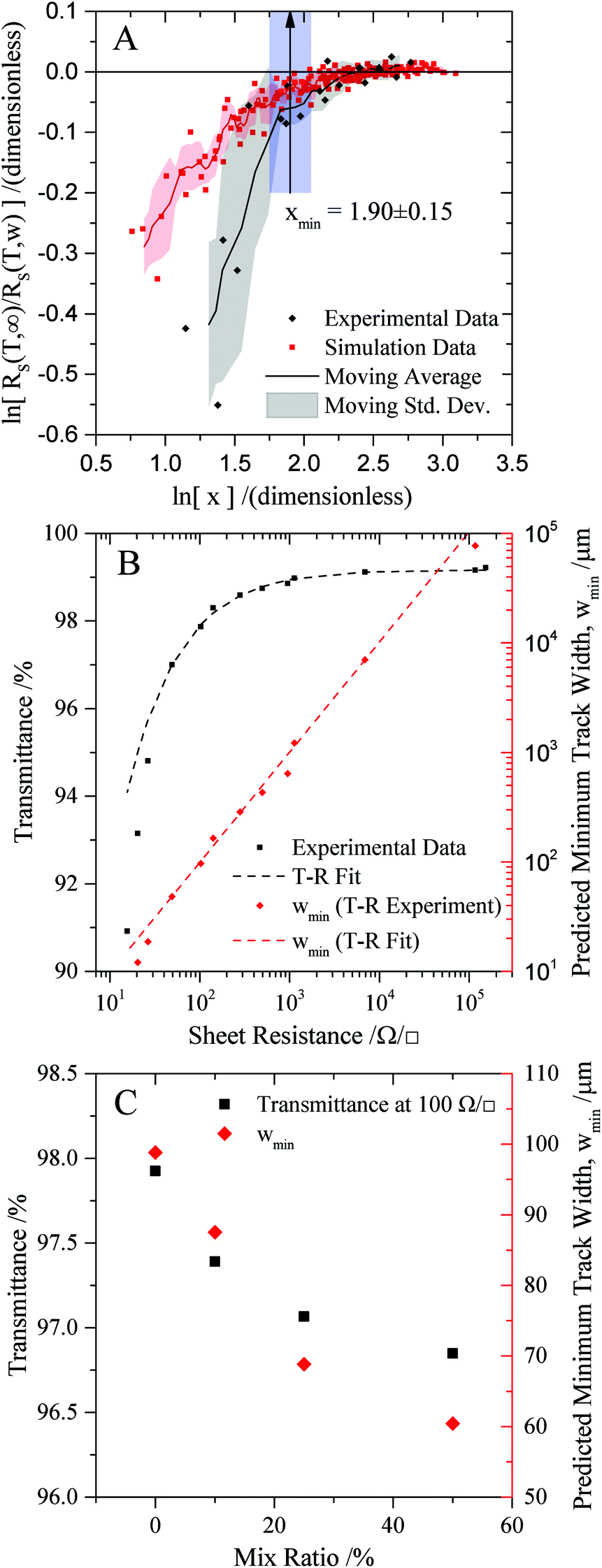 | ||
| Fig. 4 (A) Plot of ln[RS(T, ∞)/RS(T, w)] against ln[x], illustrating an estimation of xmin. Points represent experimental and simulation data; solid lines are five-point moving averages; shaded areas are five-point moving standard deviations. (B) T–R curve for as-received AgNWs, with a comparison to the minimum feature size predicted by eqn (4). Data points represent direct measurements (T–R) and predictions based on the experimental data (track width). Dashed lines represent values calculated based on the fitted values of eqn (3) to the data. (C) Plot of both the transmittance at 100 Ω □−1 and predicted minimum feature size wmin against the volume ratio of short (sonicated) to long (unsonicated) nanowire dispersions. | ||
It is evident from the data in Fig. 4(B) that this analysis places a restriction on the size of a film over which a T–R data series may be considered reliable; for values of RS ≥ 10 kΩ □−1 (in this specific case) the sample must have a minimum dimension in the range of 1 to 10 cm (for measurements of RS; values of T may be sampled over smaller areas provided that the material is uniformly deposited).
Fig. 4(C) demonstrates the value of mixing short and long nanowire populations. Although it is well established that reducing the mean length of a nanowire population produces qualitatively “inferior” films (in terms of their T–R curves),6 we see here that there is a trade-off available in terms of device design. By sacrificing 1% of the film transmittance at 100 Ω □−1, it is possible to obtain 40% smaller feature sizes in this specific case. This type of compromise may prove important in applications where the feature size and sheet resistance are dominant requirements over the film transmittance.
Thus far we have only considered pristine silver nanowire films. However there are examples in the literature of post-processing used to optimise film properties. It is understood that the NW–NW junction resistance is a dominant factor in determining RS;23 as such many researchers have developed processes for reducing the junction resistance.23–26 The finite-size scaling effect described in this work is, in a certain sense, a ‘geometrical’ property of the nanowire network at a given density. That is, provided post-processing affects only the distribution of junction resistances (and avoids adding new current paths), at a fixed density the predicted value of wmin should remain unchanged. However the act of lowering the junction resistance allows for the formation of films with equivalent sheet resistance using a lower material density. While this leads to an improvement in T–R performance (raising T at a fixed RS), we would anticipate that it will also increase wmin which may be undesirable depending on the application in question. As such there will be a trade-off between obtainable values of T, RS and wmin.
Looking towards the most restrictive devices in terms of transparent conductive film parameters, displays such as LCD and OLED panels, we may ask ourselves; what is necessary to make silver nanowires compatible with such applications? Modern mobile devices typically have the highest display resolutions, of 400 to 500 ppi (pixels per inch); this corresponds to a pixel pitch of 50 to 65 μm and therefore sub-pixel elements are likely to be of the order of 15 to 20 μm in size. For the material used in this study, we can suggest from Fig. 4(B) that a film with RS ≈ 10 Ω □−1 and T = 90% may be able to satisfy that requirement. This performance is comparable to that of state-of-the-art ITO films developed recently.20,21 For less stringent display applications such as televisions and computer monitors, where the pixel pitch tends to be higher (resolution between 200 and 300 ppi), we suggest that AgNWs are in principle able to compete with ITO based on this particular consideration. While prior demonstrations of LCD cells using AgNW electrodes exist,22 we believe that this is one of the first indications that these materials may be compatible with existing device architectures.
4. Conclusions
We have demonstrated an analysis of the finite-size scaling behaviour of practical silver nanowire films, considering the effects due to systematic variation of the nanowire length distribution. We find a design rule that allows a restriction to be placed on the minimum feature size used in a device design in order to maintain the sheet resistance of a large area film. As a result, it is evident that there is a trade-off available between film transmittance, sheet resistance, and minimum feature size which can be modified by manipulation of the nanowire length distribution.We suggest that with a minimum investment in experimental measurements (i.e. collection of T–R data series) it is possible to screen different nanowire materials in order to find candidates suitable for a given application, where a device design already exists. Alternatively, such information about a material may be used to elucidate the implications for device design.
Acknowledgements
The authors would like to gratefully acknowledge funding from M-Solv Ltd. This work was supported by the Engineering and Physical Sciences Research Council (EPSRC, grant numbers EP/K031562/1 and EP/M507775/1).References
- IDTechEx, Transparent Conductive Films (TCF) 2015–2025: Forecasts, Markets, Technologies, 2015, http://www.idtechex.com/tcf, (accessed June 2016).
- S. De, P. J. King, P. E. Lyons, U. Khan and J. N. Coleman, ACS Nano, 2010, 4, 7064–7072 CrossRef CAS PubMed.
- V. Scardaci, R. Coull, P. Lyons, D. Rickard and J. Coleman, Small, 2011, 7, 2621–2628 CrossRef CAS PubMed.
- S. Bergin, Y.-H. Chen, A. Rathmell, P. Charbonneau, Z.-Y. Li and B. Wiley, Nanoscale, 2012, 4, 1996–2004 RSC.
- S. Sorel, P. Lyons, S. De, J. Dickerson and J. Coleman, Nanotechnology, 2012, 23, 185201 CrossRef PubMed.
- R. Mutiso, M. Sherrott, A. R. Rathmell, B. J. Wiley and K. I. Winey, ACS Nano, 2013, 7, 7654–7663 CrossRef CAS PubMed.
- D. Stauffer and A. Aharony, Introduction to percolation theory, Taylor & Francis, London, 1994 Search PubMed.
- S. Hong, J. Yeo, J. Lee, H. Lee, P. Lee, S. S. Lee and S. H. Ko, J. Nanosci. Nanotechnol., 2015, 15, 2317–2323 CrossRef CAS PubMed.
- M. Cann, M. Large, S. Henley, D. Milne, T. Sato, H. Chan, I. Jurewicz and A. Dalton, Mater. Today Commun., 2016, 7, 42–50 CrossRef.
- ImageJ: Image Processing and Analysis in Java, http://imagej.nih.gov/ij/, (accessed June 2016).
- S. Henley, M. Cann, I. Jurewicz, A. Dalton and D. Milne, Nanoscale, 2014, 6, 946–952 RSC.
- J. T. Li and S.-L. Zhang, Phys. Rev. E: Stat. Phys., Plasmas, Fluids, Relat. Interdiscip. Top., 2009, 80, 040104(R) CrossRef PubMed.
- J. Li and S.-L. Zhang, Phys. Rev. E: Stat. Phys., Plasmas, Fluids, Relat. Interdiscip. Top., 2010, 81, 021120 CrossRef PubMed.
- J. Li and M. Östling, Phys. Rev. E: Stat. Phys., Plasmas, Fluids, Relat. Interdiscip. Top., 2012, 86, 040105 CrossRef PubMed.
- M. Large, J. Burn, A. King, S. Ogilvie, I. Jurewicz and A. Dalton, Sci. Rep., 2016, 6, 25365 CrossRef PubMed.
- Lumerical Solutions, FDTD Solutions, http://www.lumerical.com/tcad-products/fdtd/, (accessed June 2016).
- S. Mertens and C. Moore, Phys. Rev. E: Stat. Phys., Plasmas, Fluids, Relat. Interdiscip. Top., 2012, 86, 061109 CrossRef PubMed.
- J. Shao and D. Tu, The Jackknife and Bootstrap, Springer-Verlag, New York, 1995 Search PubMed.
- A. Margolina and H. J. Herrmann, Phys. Lett. A, 1984, 104, 295–298 CrossRef.
- U. Betz, M. Kharrazi Olsson, J. Marthy, M. F. Escolá and F. Atamny, Surf. Coat. Technol., 2006, 200, 5751–5759 CrossRef CAS.
- T. Minami, Thin Solid Films, 2008, 516, 5822–5828 CrossRef CAS.
- H.-G. Park, G.-S. Heo, S.-G. Park, H.-C. Jeong, J. Lee and D.-S. Seo, ECS Solid State Lett., 2015, 4, R50–R52 CrossRef CAS.
- D. Langley, M. Lagrange, G. Giusti, C. Jiménez, Y. Bréchet, N. Nguyen and D. Bellet, Nanoscale, 2014, 6, 13535–13543 RSC.
- I. Jurewicz, A. Fahimi, P. Lyons, R. Smith, M. Cann, M. Large, M. Tian, J. Coleman and A. Dalton, Adv. Funct. Mater., 2014, 24, 7580–7587 CrossRef CAS.
- Y.-J. Shiau, K.-M. Chiang and H.-W. Lin, Nanoscale, 2015, 7, 12698–12705 RSC.
- J.-H. Chang, K.-M. Chiang, H.-W. Kang, W.-J. Chi, J.-H. Chang, C.-I. Wu and H.-W. Lin, Nanoscale, 2015, 7, 4572–4579 RSC.
Footnote |
| † Electronic supplementary information (ESI) available: Description of percolation simulation algorithm; details of statistical processing of experimental measurements; further detail of finite-size scaling theory as it applies to AgNW films. See DOI: 10.1039/C6NR03960J |
| This journal is © The Royal Society of Chemistry 2016 |