
 Open Access Article
 This Open Access Article is licensed under a
 Creative Commons Attribution 3.0 Unported Licence
Ultra-small photoluminescent silicon-carbide nanocrystals by atmospheric-pressure plasmas†
Sadegh
Askari
ab,
Atta
Ul Haq
a,
Manuel
Macias-Montero
a,
Igor
Levchenko
c,
Fengjiao
Yu
d,
Wuzong
Zhou
d,
Kostya (Ken)
Ostrikov
ef,
Paul
Maguire
 a,
Vladimir
Svrcek
g and
Davide
Mariotti
*a
a,
Vladimir
Svrcek
g and
Davide
Mariotti
*a
aNanotechnology & Integrated Bio-Engineering Centre, Ulster University, BT37 0QB, UK. E-mail: d.mariotti@ulster.ac.uk
bDepartment of Physics, Chemistry and biology (IFM), Linköping University, SE-581 83 Linköping, Sweden
cSchool of Chemistry, Physics and Mechanical Engineering, Queensland University of Technology, Brisbane QLD 4000, Australia
dEaStChem, School of Chemistry, University of St Andrews, St Andrews, KY16 9ST, UK
eInstitute for Future Environments and School of Chemistry, Physics and Mechanical Engineering, Queensland University of Technology, Brisbane QLD 4000, Australia
fCSIRO-QUT Joint Sustainable Processes and Devices Laboratory, Commonwealth Scientific and Industrial Research Organization, P.O. Box 218, Lindfield, NSW 2070, Australia
gResearch Center of Photovoltaics, National Institute of Advanced Industrial Science and Technology-AIST, Central 2, Tsukuba, Japan
First published on 23rd September 2016
Abstract
Highly size-controllable synthesis of free-standing perfectly crystalline silicon carbide nanocrystals has been achieved for the first time through a plasma-based bottom-up process. This low-cost, scalable, ligand-free atmospheric pressure technique allows fabrication of ultra-small (down to 1.5 nm) nanocrystals with very low level of surface contamination, leading to fundamental insights into optical properties of the nanocrystals. This is also confirmed by their exceptional photoluminescence emission yield enhanced by more than 5 times by reducing the nanocrystals sizes in the range of 1–5 nm, which is attributed to quantum confinement in ultra-small nanocrystals. This method is potentially scalable and readily extendable to a wide range of other classes of materials. Moreover, this ligand-free process can produce colloidal nanocrystals by direct deposition into liquid, onto biological materials or onto the substrate of choice to form nanocrystal films. Our simple but efficient approach based on non-equilibrium plasma environment is a response to the need of most efficient bottom-up processes in nanosynthesis and nanotechnology.
1. Introduction
Elemental silicon nanocrystals (NCs) have been proposed as a promising material for optoelectronic, biomedical imaging and diagnostic applications.1–3 Additional important features can be achieved by alloying silicon, for instance with carbon. In the bulk form, silicon carbide (SiC) is known as a chemically inert, extremely hard, key material for high power, high frequency and high temperature electronic devices and it is recognized as a candidate for next generation photonics and electronics.4–9The origin of photoluminescence in NCs in general can vary dramatically depending on the surface states and degree of quantum confinement. In SiC NCs, as well as in most Si-based NCs, the photoluminescence origin and its performance is further complicated by potential transitions between direct and indirect behaviour. However, while this represents a complex system to be studied, it can also offer important application opportunities. New findings show that SiC is an excellent material for single photon emitters and quantum computation, for instance through the incorporation of defects in SiC nanoparticles.5
SiC is a poor light emitter in the bulk form due to its indirect bandgap. Efficient and stable photoluminescence has been now reported from SiC NCs in the range from ultra-violet to yellow.10–14 This feature has triggered research on SiC NCs with a range of potential applications including biomedical applications.10,13–16 In opposition to silicon NCs, Si–C bonds makes SiC NCs chemically stable and thus additional surface passivation is not needed. SiC NCs are dispersible in different liquids including water that allows preparing clear colloids from small NCs (<5 nm) for living cell applications. Therefore, size-dependent, efficient and stable photoluminescence combined with the advantageous material properties of SiC, makes SiC NCs highly attractive candidates for a very wide range of applications.
However, the synthesis of SiC NCs is extremely challenging due to the high melting temperature and hardness of bulk silicon carbide. Electrochemical etching of solid SiC wafers or wet chemical etching of SiC powder is often used10,12 but significant limitations such as the need for strong acids (e.g. hydrofluoric acid), expensive raw materials (crystalline high-purity SiC wafers) and considerable nanocrystal aggregation still exist. Furthermore, these traditional methods do not ensure sufficient level of control over the NCs properties and in particular, over the size distribution, which requires additional size-selective steps. These challenges impede a wide use of SiC NCs in many state-of-the-art applications. Unfortunately, attempts to modify or enhance the above described methods did not lead to the significant boost of SiC NCs characteristics, since the main drawbacks are the manifestations of top-down nature of the methods used.
Here we present a gas phase method based on atmospheric pressure plasma, which for the first time demonstrates ligand-free synthesis of highly crystalline ultra-small (down to 1.5 nm) SiC NCs and can address the current synthesis challenges. Specifically, we report size-controlled fabrication of free-standing SiC NCs with efficient photoluminescence without any further surface chemical treatment. The method is a convenient, environmentally friendly, inexpensive one-step process with an apparent potential for scalability. Furthermore, the accurate control over the NCs size has allowed for the first time to reveal important insights into the crystal structure and nanocrystal optical properties.
2. Results and discussion
2.1. Description of the experimental set-up
A schematic diagram of the plasma reactor used for the synthesis of SiC NCs is shown in Fig. 1a. Fig. 1b shows the photo of the plasma reactor and discharge and Fig. 1c is a typical transmission electron microscopy (TEM) image of the synthesized SiC NCs. The plasma was generated within a rectangular glass tubing with an internal cross section of 0.5 mm × 5 mm (0.3 mm wall thickness). Two identical copper electrodes placed at both sides of the rectangular glass tubing formed the contact area of 5 mm × 20 mm between the copper electrodes and the glass tubing. Therefore the volume of the plasma is determined by the electrode-glass contact area and the 0.5 mm internal tubing gap. The plasma is sustained by radio frequency (RF) power at 13.56 MHz. The gas flow direction is along the longer length of the plasma, i.e. along the 20 mm long electrode side. The background gas for sustaining the plasma is argon. Tetramethylsilane (TMS), used as precursor, was delivered to the reactor using a bubbler with a given flow of argon bubbling through it, hereafter TMS flow. The results presented in this paper relate to three different flow rates of argon through the bubbler: 0.4 sccm, 2.4 sccm and 5.0 sccm. The total gas flow rate through the reactor was maintained constant at 1000 sccm and the applied RF power is fixed at 100 W. The plasma reactor was installed in a nitrogen-filled stainless steel chamber to provide controlled experimental conditions and avoid air contamination (see ESI, Fig. S1†).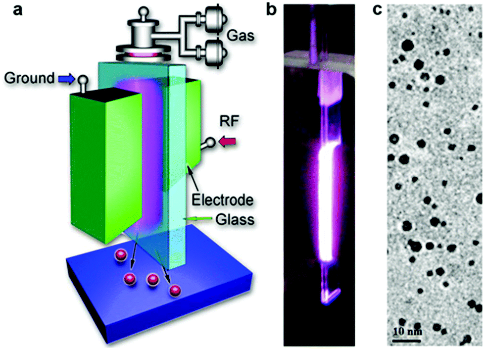 | ||
| Fig. 1 (a) Schematic diagram for the atmospheric pressure plasma reactor (RF stands for radio frequency). (b) Side-view photo showing the ignited plasma (gas flow is in the up-down direction). (c) Typical transmission electron microscopic image of the nanoparticles produced with 5 sccm argon flow through the bubbler. | ||
2.2. Material characterization
The bubbler was used to control the flow and concentration of TMS in the plasma, and eventually, the size of the NCs. Typical TEM images of the samples of different sizes are presented in Fig. 2. Fig. 3 reports the corresponding size distributions determined by TEM analysis (∼500 NCs per sample were considered); these were then used to produce log-normal fits and corresponding geometric means (Dp) and standard deviations (σ) at the different synthesis conditions.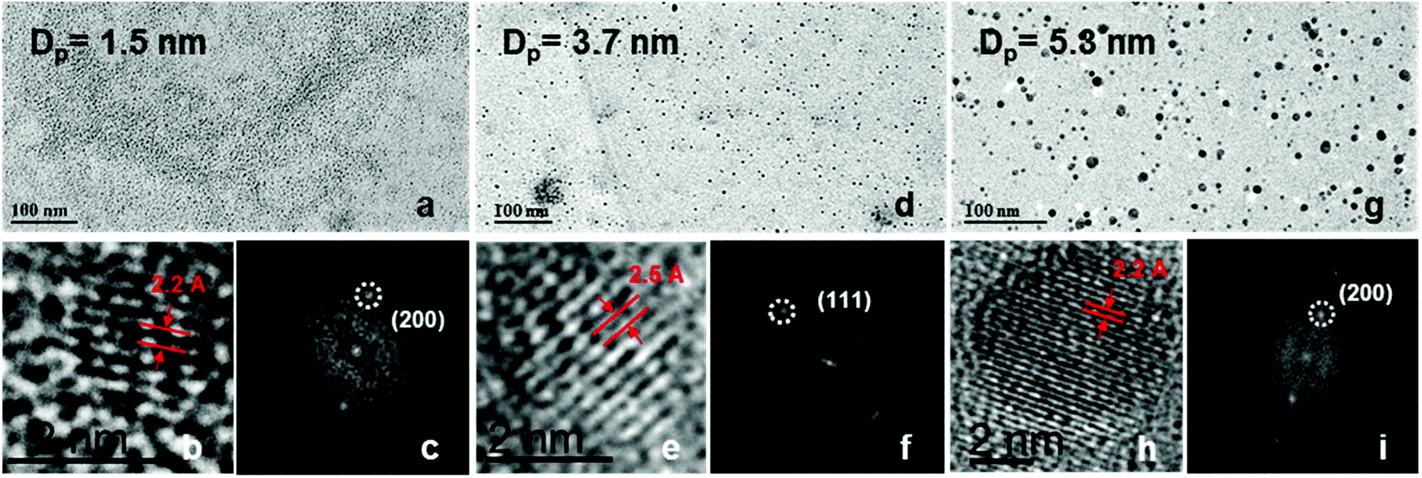 | ||
| Fig. 2 Transmission electron microscopy, (a, d, g) low magnification and (b, e, h) high resolution images with corresponding (c, f, i) fast Fourier transform (FFT) analysis for SiC nanocrystals produced at three different precursor flow conditions: (a–c) 0.4 sccm, (d–f) 2.4 sccm and (g–i) 5 sccm, where the lattice spacing of the high resolution images are 0.22 nm, 0.25 nm and 0.22 nm, respectively. | ||
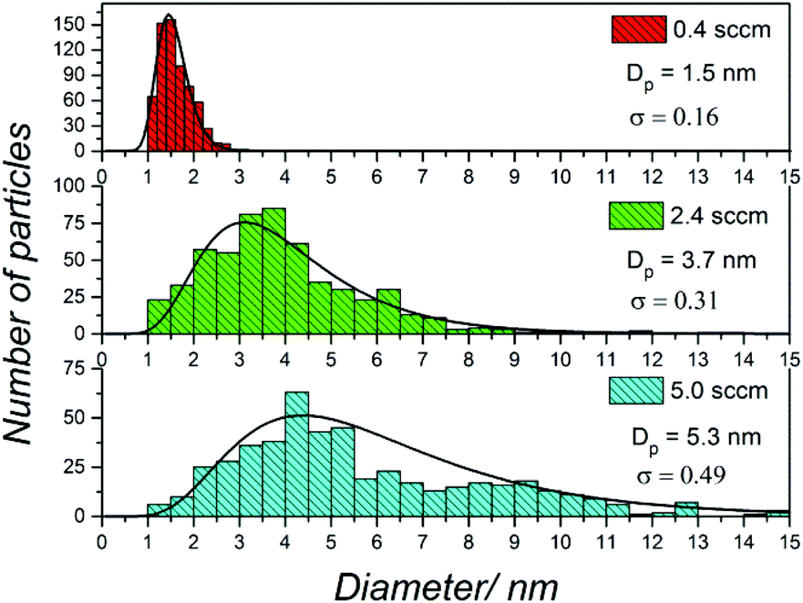 | ||
| Fig. 3 Size distribution determined from transmission electron microscopy (TEM) images of SiC nanocrystals (NCs) produced at three different precursor flow conditions (0.4 sccm, 2.4 sccm and 5 sccm), which correspond to the TEM images shown in Fig. 2. The geometric mean value (Dp) and standard deviation (σ) determined by fitting the experimental distribution with a log normal distribution are also provided. | ||
The size distribution for all three conditions fit log-normal distributions which have been observed frequently from NCs synthesised in atmospheric pressure plasma17,18 or other methods.19Fig. 2a–c shows TEM results for a sample prepared with 0.4 sccm TMS flow rate, which produced spherical and very well separated NCs. The corresponding size distribution of the NCs under this synthesis condition (Fig. 3, top) shows that NCs have a fairly narrow distribution with a mean diameter of 1.5 nm. The TEM results for a sample produced with 2.4 sccm TMS flow are shown in Fig. 2d–f with corresponding size distribution in Fig. 3 (middle). Also in this case, the NCs are very well separated and have a narrow size distribution with 3.7 nm mean size. Finally, with 5 sccm TMS flow, larger NCs can be produced (Fig. 2g–i) with a mean diameter of 5.3 nm (Fig. 3, bottom). The TEM results confirm the relationship between TMS flow and size of the NCs, whereby a higher flow (i.e. higher TMS concentration) leads to larger NCs. The size analysis shows that smaller particles are easier to produce with a narrower distribution; nonetheless, our results still show better size control than other methods reported in the literature.20
SiC exhibits strong polytypism with hundreds of crystalline structures and varying stacking sequences.21,22 SiC polytypes have identical arrangements in the two dimensions of the hexagonal basal plane and are different in the third dimension of the Si–C bilayer perpendicular to the basal plane. Three of the most frequent and most important polytypes result from pure cubic (β) stacking (3C-SiC) and hexagonal (α) stacking (specifically, 4H-SiC and 6H-SiC), which correspond to the zinc-blende and wurtzite structures. However, the identification of the polytype in NCs, compared to bulk SiC, has to be approached with caution for two reasons. Firstly, the limited number of planes can make it difficult to clearly observe diffraction, especially for the 4H or 6H hexagonal crystal structure. For the same reason X-ray diffraction analysis may not produce a clear spectrum also due to substantial broadening of the peaks.21,23 Secondly, lattice spacing and crystal structure of NCs (especially for NCs in the strong quantum confinement regime) is expected to deviate from the known bulk configurations due to surface reconstruction; this may prevent altogether the formation of the same polytypes as found in bulk SiC.20–23
From a theoretical point of view, the definition of the cubic or hexagonal crystal structures only makes sense for an extended repetition of the crystal planes; crystal structures become identical when the number of crystal planes is limited.21,24 For NCs with sizes below ∼1 nm in diameter, only one crystal structure exists,20,24 while for NCs with larger diameters (∼1–3 nm), both 4H-SiC and 6H-SiC are expected to be identical. In the latter case the number of planes may be sufficient to differentiate, at least in principle, the hexagonal structures from the 3C-SiC crystal structure; however all three structures may appear very similar due to experimental limitations. Particles with diameter above ∼3 nm may then present fully developed crystals structures with a sufficient number of planes for 3C-, 4H- and 6H-SiC polytypes to establish their characteristic crystalline configurations.
TEM analysis of our samples has revealed lattice spacings close to 0.22 nm (e.g.Fig. 2b and h) which could be indexed to either the (200) planes or the (104) planes of the 3C-SiC or hexagonal SiC, respectively.20,25 Spacing of 0.25 nm (e.g.Fig. 2e) were also found that belongs to the (111) planes of 3C-SiC with a cubic unit cell parameter of 0.43591 nm.25 These lattice spacing values and plane assignments are confirmed by fast Fourier transform analysis (FFT) of the corresponding high resolution images (Fig. 2c, f and i). No particular relationship was however found between the size and the frequency of any of the lattice spacing. These observations support the assignment of a cubic crystal structure as more probable than the hexagonal one for all NCs considering that (104) planes have generally very low probability of being observed.20,21 The diffraction patterns of SiC NCs ensembles is in full agreement with the assignment of the 3C-SiC crystal structure for NCs produced at all three different synthesis conditions (see ESI, Fig. S2†). For all NCs produced here, the crystal structure is also consistent with the chemical composition of SiC NCs.
The chemical composition is further confirmed by Fourier transform infrared spectroscopy (FTIR) and X-ray photoelectron spectroscopy (XPS), see Fig. 4. A typical FTIR spectrum is presented in Fig. 4a for the SiC NCs produced at 2.4 sccm TMS flow corresponding to a mean diameter of 3.7 nm. The FTIR of SiC NCs synthesized at other conditions (not shown) produced the same features as shown in Fig. 4a. Several major bands are observed; the strongest band is at ∼780 cm−1 and is attributed to the Si–C stretching mode.26,27 The predominance of this peak confirms the formation of Si–C bonds and corroborates the SiC crystal structure identified by TEM. The peak at 1020 cm−1 can be assigned to C–H2 wagging in Si–[CH2]n–Si bonds.28 Absorption from Si–O–Si and/or Si–O–C asymmetric stretching is also possible in this range however they generally exhibit a broader feature due to varying stoichiometric arrangements.29,30 The 1254 cm−1 peak can be attributed to CH2 (or CH3) symmetric bending mode in [Si–CH2/3]n groups.28 Si–H stretching modes can be seen around 2110 cm−1.1 The weak peaks around 1400 cm−1 could be attributed to the C–CH3 bonds as the methyl asymmetric and symmetric bending in C–CH3 gives absorbance peaks at 1460 cm−1 and 1375 cm−1.30,31 The band in the range 2850–3000 cm−1 is typical of C–H stretching in –CH3 and –CH2 groups.28,31
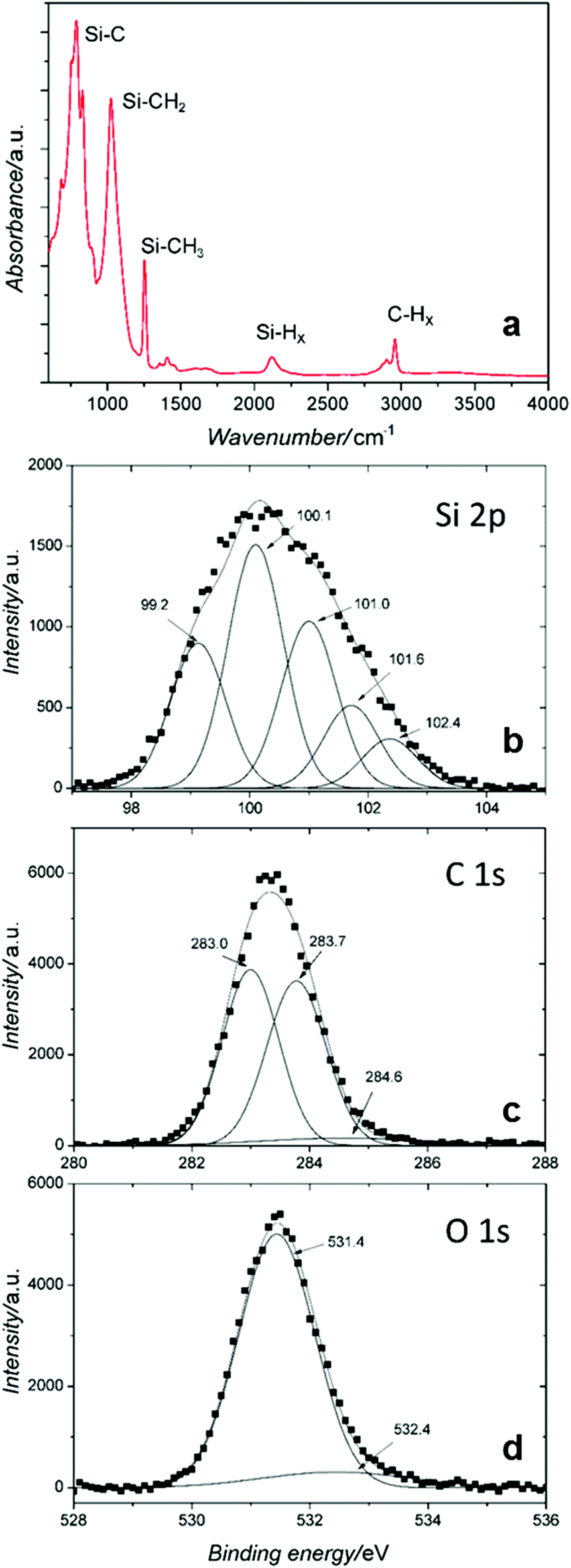 | ||
| Fig. 4 (a) Fourier transform infrared spectrum of SiC nanocrystals produced with 2.4 sccm precursor flow. (b–d) High resolution X-ray photoelectron spectra of SiC nanocrystals. (b) The Si 2p peak is formed by five peaks: Si–Si or/and Si–H at 99.2 eV, high- (101.0 eV) and low-coordinated (100.1 eV) Si–C bonds, O–Si–C at 101.6 and Si–O at 102.4 eV. (c) C 1s is fitted with high-coordinated C–Si at 283.0 eV, C–H at 283.7 eV and C–C at 284.6 eV. (d) O 1s is fitted with O–Si–C at 531.4 eV and high coordinated O–Si at 532.4 eV. | ||
Fig. 4b–d show high-resolution XPS profiles of the sample produced at 2.4 sccm TMS flow for the three main peaks: Si 2p, C 1s and O 1s. The spectral deconvolution of the peaks is carried out by fitting Gaussian curves. The Si 2p core peak consists of five peaks assigned to Si–Si or/and Si–H (99.2 eV), low- and high-coordinated Si–C bonds (100.1 eV and 101.0 eV), O–Si–C (101.6 eV) and Si–O (102.4 eV),26,31 which again confirm the presence of Si–C bonds. The C 1s is deconvoluted into two strong peaks from high-coordinated C–Si (283 eV) and C–H bond (283.7 eV); the low C–C peak at 284.6 eV confirms the majority of Si–C core bonds.26,31 The O 1s curve is fitted well with the profile from O–Si–C bond (531.4 eV) and high-coordinated Si–O at 532.4 eV is essentially absent.
The overall combined XPS-FTIR results support the TEM analysis suggesting the formation of SiC NCs due to Si–C bonds observed throughout. The XPS Si 2p peak at 99.2 eV may suggest the presence of Si–H surface terminations, however also C–H terminations are observed (XPS C 1s peak at 283.7 eV and also FTIR absorption, see Fig. 4c and a, respectively). Different terminations may arise at different facets of the NCs whereby oxidation is very limited and seem to have taken place only at the Si–H terminated surface; selective and minor oxidation is supported by the O 1s peak attributed to Si–O with carbon backbond (i.e. C–Si–O) and the absence of Si–O absorption in the FTIR around 1100 cm−1. The chemical and crystal structure of the NCs has an impact on their optical properties and in particular on the PL emission.
2.3. Photoluminescence of the SiC nanocrystals
The PL emission of SiC NCs has been attributed to molecular transitions in some cases due to defects,32 bandgap transitions that are affected by quantum confinement (QC) or transitions taking place at the surface that may also be affected by QC.12,33 The role of QC in PL emission of SiC NCs has been under debate.23,32,34,35 One reason has been the lack of a synthesis method with accurate control over size of NCs. Support for QC has mostly been based on the PL peak shift when excited at different wavelengths.11,12,36 However, this evidence is not conclusive as surface defects can lead to similar behavior. It is noteworthy that the surface of NCs produced using etching methods is heavily passivated with bonded oxygen (O and OH bonds) which influences their optical properties. Previous computational studies confirms the sensitivity of the PL originating from defect states and surface terminations, which in turn depends on the preparation methods.22,37,38QC is expected to influence various properties of NCs when the size approaches the corresponding Bohr exciton radius. However the Bohr radii and optical properties strongly depend also on the crystal structure.24 For instance a bandgap of ∼2.20–2.35 eV (3C-SiC, cubic),20,21,32,34 ∼3.30 eV (4H-SiC, hexagonal)20,21 or 2.86–3.02 eV (6H-SiC, hexagonal)20,23 has been observed for the different polytypes. The corresponding Bohr radii are 2.0 nm (3C-SiC),20,23 1.2 nm (4H-SiC)20 and 0.7 nm (6H-SiC),20,23 respectively. Due to the absence of different polytypes for ultra-small NCs, the bandgap, Bohr radii, quantum confinement effects and optical properties are expected to converge into behaviors that closely resemble that of 3C-SiC NCs as the diameter is reduced.20
On the basis of our size and crystal structure analysis, our smallest SiC NCs have a mean radius (1.5 nm/2 = 0.75 nm) comparable with or smaller than the Bohr radii of all polytypes, so that regardless of its crystal structure we should expect QC effects, e.g. increased PL intensity and widening of the bandgap. As these 1.5 nm diameter NCs are likely to resemble a 3C-SiC crystal structure, a strong QC is very likely. A degree of quantum confinement should also be observed in the NC with mean diameter of 3.7 nm (1.85 nm radius), which is also smaller than the 2.0 nm Bohr radius of 3C-SiC. Finally, the largest NCs with 5.4 mean diameter and a 3C-SiC crystal structure will likely present bulk-like optical properties with the characteristic weak luminescence of indirect bandgap bulk SiC.23
The PL spectra for different excitation wavelengths (230–280 nm) of the NCs dispersed in ethanol are shown in Fig. 5. The overall emission intensity increases with increasing excitation wavelength. This is in part due to the excitation source having different intensities at different wavelengths so that the emission is normally overall stronger for longer excitation wavelengths that have stronger excitation intensity. While generally PL results could be normalized, in Fig. 5 we preferred to present the data in its raw format for clarity and to prevent the different emission curves to overlap. In addition, the increasing trend is also partly due to the excitation wavelength approaching the energy of the emission peaks whereby emitting states are more efficiently excited when the excitation energy is above but close to the corresponding energy. The PL profile of the smallest NCs (mean diameter 1.5 nm with 0.4 sccm TMS flow) comprises two major emission bands peaking with multiple peaks at 300–360 nm and at 409 nm. The position of the emission peaks are not visibly shifted for the different excitation wavelengths (see also ESI†). The PL profile of the larger NCs (Fig. 5b and c) is similar to that of the smaller NCs except that the emission at 375–450 nm is absent; as it can be seen in Fig. 5a–c (and also in the ESI†), the position of the peaks at about 306.8 nm, 323.5 nm, 335.0 nm and 356.8 nm is unchanged for NCs with different sizes.
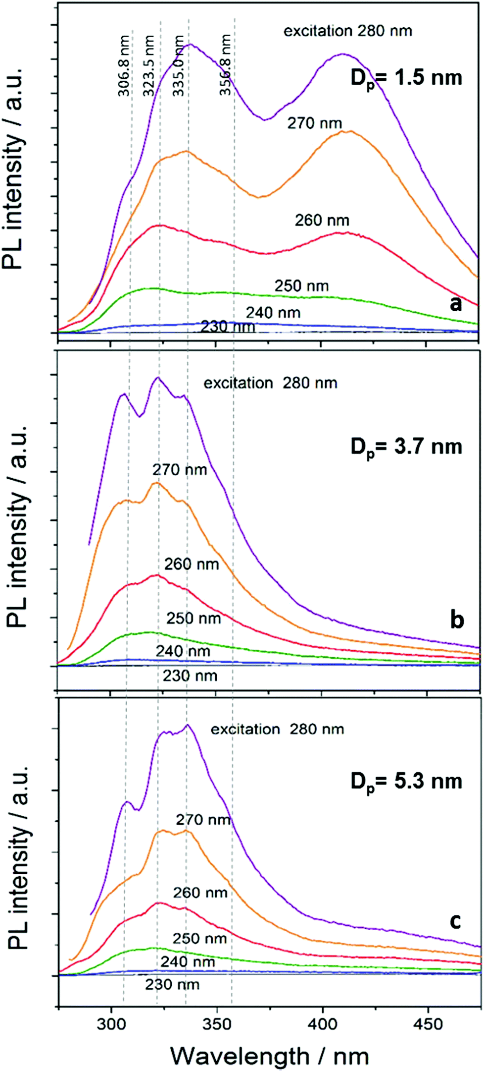 | ||
| Fig. 5 Photoluminescence spectra of SiC nanocrystals with three different mean diameter 1.5 nm (a), 3.7 nm (b) and 5.3 nm (c) dispersed in ethanol. The excitation wavelength varies in the range 230–280 nm. | ||
The multiple peaks appearing in all spectra of Fig. 5 in the range 300–360 nm have not been observed before and have not been discussed in the literature. At the same time, the synthesis conditions and controlled quality of these SiC NCs exceeds that of NCs produced with other methods. At this time we are therefore unable to conclusively assign the origin of this emission band, however the regular multi-peak structure at fixed wavelengths suggest radiative recombination at the surface. If defect states were present, these would be located in the gap and therefore expected to emit in the red part of the spectra. Furthermore, our NCs do not exhibit any other evidence of defect states as found in other NCs (see further below). Despite the size distribution, no shift occurs in the PL upon changing the excitation wavelength. It follows that, most likely, this emission originates from surface states with similar terminations and due to the interruption of the stacking sequence. The four main peaks (356.8 nm, 335.0 nm, 323.5 nm and 306.8 nm) correlate with the luminescence of stacking faults39 from irregular stacking sequences that are enhanced as the diameter and surface area of the NCs is increased. Indeed, it is expected and calculations show that H-terminated NCs of this size should emit in this region.37
The peak at 409 nm (∼3 eV) in Fig. 5a is believed to be the result of bandgap transitions. This is supported by the bulk bandgap value of 2.20–2.35 eV for 3C-SiC, which is increased to ∼3 eV due to quantum confinement in NCs with 1.5 nm mean diameter. This is also consistent with theoretical and experimental results found in the literature (see further below).32,34,37 The peak maximum does not exhibit any noticeable shift mainly due to the very narrow size distribution (Fig. 3-top) and weak excitation dependence of ultra-small NCs.20 PL emission in this range (400–500 nm) was previously associated to 6H polytype inclusions and related stacking faults of 4 nm diameter NCs.32 In our 1.5 nm diameter NCs, however, the development of a 6H stacking sequence is not possible as demonstrated by our TEM analysis. Furthermore, defect-related emission typical of hexagonal structure generally includes stronger peaks at ∼430–450 nm,20,23,32,34 which are not observed in our samples and corroborates the absence of defects and the cubic crystal structure of our 1.5 nm mean diameter NCs.
The larger NCs (Fig. 5b and c) do not show any defect-related emission in the range 400–500 nm nor bandgap transitions since quantum confinement is expected to be weak (3.7 nm NCs) or non-existent (5.3 nm NCs). This is further confirmed by the emission yield of NCs being drastically reduced with increasing the NCs size. We measured the absolute PL quantum yield (QY) for the NCs deposited on quartz substrates and excited with the laser beam at wavelength 280 nm. The values obtained are 13.2%, 8.4% and 2.6% for the NCs with a mean diameter 1.5 nm, 3.7 nm and 5.3 nm, respectively. The higher QY for the smaller NCs is further evidence of QC effects with values similar to that reported for a number of SiC NCs and some other direct bandgap quantum dots.20,23
In order to produce emission originating from bandgap transitions of the larger NCs we have excited the samples with a longer wavelength (365 nm). Excitation at 365 nm is more efficient in producing PL emission of larger NCs because it is closer to their expected PL peak wavelength and it avoids the excitation of high energy states (300–360 nm) observed in Fig. 5. In Fig. 6 (obtained with 365 nm excitation), the PL emission peaks at 555 nm and 564 nm for the NCs with mean diameter of 3.7 nm and 5.3 nm, respectively. The non-symmetric shape of the PL emission of these two samples is due to the 400 nm cut-off filter used for these measurements, required to prevent the strong excitation reaching the detector. The dashed lines in Fig. 6 show the corresponding Gaussian fits to the curves and clarify the effect of the cut-off filter. If we consider the Gaussian fits, the PL of the two samples peak at 537 nm (3.7 nm NCs) and 550 nm (5.3 nm NCs), which correspond to a bandgap of ∼2.3 eV and ∼2.2 eV, respectively. These peak wavelengths are in good agreement with the expected bandgap of 3C-SiC, with weak or no confinement for the 3.7 nm and 5.3 nm NCs. The PL emission for the sample with the 1.5 nm mean diameter NCs is also included in Fig. 6 and is consistent with our previous measurement of Fig. 5a. However, in Fig. 6 the PL emission at 409 nm is highly distorted by the non-linear cut-off filter.
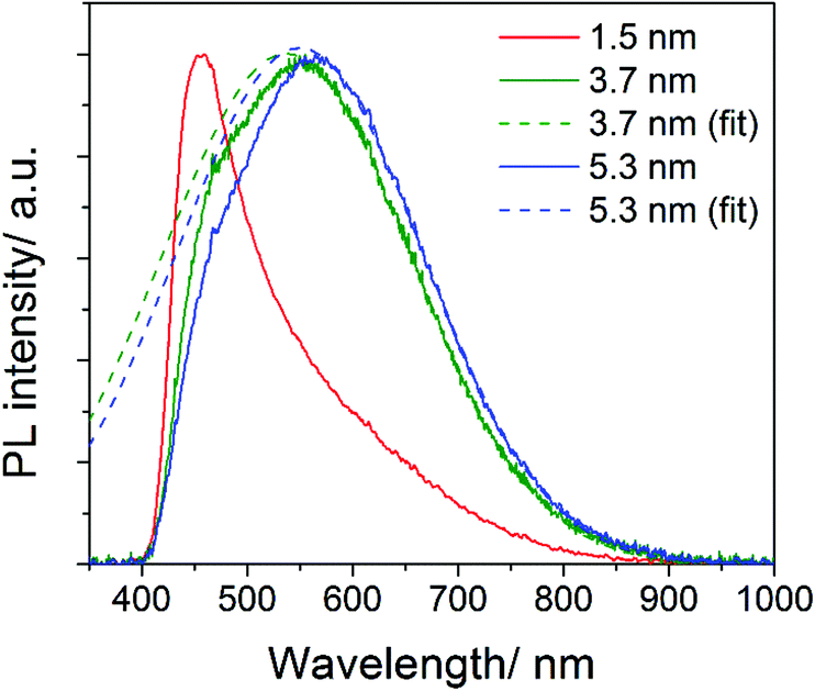 | ||
| Fig. 6 Photoluminescence (PL) spectra of SiC nanocrystals with three different mean diameters dispersed in ethanol. The excitation wavelength is 365 nm. The measurements included a 400 nm cut-off filter which distorts the PL emission. Gaussian fits have been produced for two of the curves. | ||
Our measurements therefore suggest bandgaps close to 3.0 eV, 2.3 eV and 2.2 eV for our NCs with mean diameter of 1.5 nm, 3.7 nm and 5.3 nm, respectively. Theoretical calculations predict the bandgap to increase to 6.2 eV, 2.65 eV or 2.485 eV for NCs with diameters of 0.5 nm, 1.83 nm or 8 nm,32,34 respectively, which are consistent with our findings. Experimental results reported in the literature have attributed bandgap emission with energies of 2.8 eV, 2.64 eV or 2.39 eV for NCs with diameters of 1.5 nm, 1.83 nm or 4 nm, respectively.32,34 Also these experimental results are in-line with ours, although some differences may exist due to different surface characteristics as well as differences in the size measurements.
It is interesting that the emission band of the larger SiC NCs with excitation at 365 nm (Fig. 6) covers almost the entire visible region and might be used for white-light emission in solid state lighting. White light is usually achieved with a trichromatic approach (mixing blue, green and red emitting NCs) and therefore white emission from the same NCs can be very attractive.40,41 Efficient luminescence from inorganic NCs is usually achieved with surface passivation with ligands or with core–shell configurations. SiC has the advantage of highly stable chemistries for a wide range of conditions therefore offering good application opportunities.
In summary, the analysis above indicates that for excitation with high energy photons, much of the recombination and photo-emission exhibit typical peaks at fixed wavelengths (300–360 nm). Only the smallest NCs are able to produce bandgap-related PL due to the strong quantum confinement and increased QY (13.2%). However, when the excitation photon energy is sufficiently small to avoid recombination at higher energy the PL from bandgap transitions of the larger NCs is also observed (Fig. 6). The peak wavelengths of the bandgap transitions for the different NCs is consistent with bandgap widening, from ∼2.2 eV (bulk-like) of the NCs with 5.3 nm mean diameter, to ∼2.3 eV of the NCs with 3.7 nm mean diameter and to ∼3.0 eV of the 1.5 nm diameter NCs. Our results also show that the synthesis method presented here enables accurate size-tunable synthesis of SiC NCs with very low levels of surface defects from oxygen contaminations; i.e. the C![[double bond, length as m-dash]](https://www.rsc.org/images/entities/char_e001.gif) O, O–Si and OH bands are absent in the FTIR spectrum and very limited oxidation is detected by XPS. This confirms that when the synthesis method allows for adequate control over the surface characteristics and size distribution, quantum confinement effects are clearly observable (e.g. increased QY and widening of the bandgap).
O, O–Si and OH bands are absent in the FTIR spectrum and very limited oxidation is detected by XPS. This confirms that when the synthesis method allows for adequate control over the surface characteristics and size distribution, quantum confinement effects are clearly observable (e.g. increased QY and widening of the bandgap).
Finally we should note that dispersiblity, stability and efficient PL of SiC NCs are important factor for applications such as biological labelling. The prepared aqueous colloids of SiC NCs are transparent and we did not observe any agglomeration or sedimentation of the NCs in our samples stored for several months.
2.4. Plasma-induced crystallization chemistry
TMS has been widely used for deposition of thin films of SiC or other compounds of Si.42–44 Spectroscopic studies of plasmas containing TMS shows that the TMS is dissociated by the plasma resulting in intermediate species including Si and Si–Hx.44,45 However full dissociation of TMS and Si atomization is required to produce the Si–C bond network because partial dissociation would “cage” Si atoms within Si–C bonds that can only lead to structures with a Si–C–C–Si network. The formation of SiC NCs demonstrates the effectiveness of our plasma design in achieving full TMS dissociation and Si atomization due to electron-induced collisions; this is further supported by optical emission spectroscopy of the TMS/argon plasma which confirms the presence of atomic Si in our plasma (see Fig. S3 in the ESI†).Following dissociation, the presence of radical species leads to initial nucleation, nanoparticle growth and crystallization. The process of crystalline particle formation is closely linked to the unique non-thermal environment involving interaction with charged species, i.e. ions and hot electrons. The crystallization process is believed to take place due to selective nanoparticle heating and due to ion and electron surface bombardment during growth,18 while the overall gas temperature remains close to room temperature. Therefore, a high density of energetic electrons plays an important role in nanoparticle crystallization in addition to efficient dissociation of the precursor. We previously demonstrated that the efficient heating of nanoparticles through interaction with the charged species in this type of plasmas can lead to the growth of Si NCs.18 The synthesis of SiC NCs here demonstrates that the formation of crystalline particles follow a very similar path for different Si-based precursors (e.g. silane and TMS).
2.5. Important features of the process
The NCs production rate, or throughput, of our current set-up was evaluated via mass measurement, for a 10 minutes deposition at 2.4 sccm TMS flow. The observed production rate of 82.8 mg h−1 is higher than the values reported for methods such as etching or laser ablation in liquid (∼10−3–1 mg h−1 has been reported for Si wafers46,47). Our current process is not optimized and we are confident NCs production rates can be increased.An important feature of this reactor configuration is its scalability: the plasma width and length (electrode-glass contact area) can be extended while maintaining the electrode gap and hence plasma conditions constant. This is important for scale-up because it allows: (i) increasing the NCs throughput (by increasing the flow) without changing the NCs size (maintaining a constant residence time and increasing the plasma length); (ii) increasing the deposition surface area that can be covered by increasing the plasma width and scanning the reactor over a substrate (or vice-versa moving the substrate under the reactor) without varying any other plasma properties (i.e. ensuring that NCs synthesis conditions are unchanged). A production rate of 1 g h−1 is therefore possible by increasing the flow by a factor of ∼12. The width of the plasma can, in principle, be extended without limit opening the prospect of orders of magnitude increase in production rates. We have already demonstrated a plasma technology with a ∼5 cm plasma width,48 which can provide ×10 improvement factor and could bring the NC throughput to 10 g h−1. A throughput of 1 kg h−1 is achievable for instance with a 5 m wide plasma or using a 2-dimensional array of smaller plasma systems; such “array” arrangements are currently used in industrial ozone generators as well as in shower-heads electrode configurations of commercial plasma system for photovoltaics.
3. Conclusions
The ligand-free synthesis of highly crystalline, ultra-small SiC NCs in a novel microplasma process was presented. The unique non-equilibrium interaction of non-thermal plasma charged species with NCs leads to the growth of crystalline nanoparticles without any agglomeration. Efficient photoluminescence was observed with reducing the NCs size to ∼1.5 nm which is attractive for biological and many other applications. The analysis of the PL emission revealed that the enhanced QY in ultra-small NCs is most likely due to quantum confinement. The method represents a simple, fast and environmentally friendly process for the synthesis of a range of high quality small nanocrystals which can be collected directly into liquids, onto biological materials or substrates for different applications. The process is scalable and suitable for high volume roll-to-roll manufacturing.4. Experimental section
For TEM analysis of the synthesised NCs a JEOL-JEM-2011 and a JEOL-JEM-2100F electron microscope were used operating at 200 kV. For TEM measurements, the NCs were collected directly from the plasma in a cuvette containing ethanol and a few drops of the colloid were drop-casted on a TEM grid. Chemical analysis is performed by FTIR and XPS using a Nicolet iS5 from Thermo Scientific equipped with an ATR iD5 and an Axis Ultra DLD spectrometer (Kratos Analytical, Japan) with monochromated Al Kα X-rays source, respectively. The PL spectra of the colloidal SiC NCs were measured with a spectrofluorometer (Horiba FluoroMax-4) with variable excitation wavelength which was selected through a monochromator. For the measurement of the PL QY, an integration sphere (Horiba Scientific Quanta) was coupled via an ultraviolet-grade optical fibre to the spectrofluorometer (Horiba FluoroMax-4) and the SiC NCs were drop-casted and dried in air on quartz substrates (5 mm × 5 mm). The excitation wavelength (280 nm) of the Xe lamp was selected through the monochromator of the spectrofluorometer. At each step, both the emission spectra from the sample and the reference (quartz substrate only) were measured and the number of emitted photons was then calculated from spectral integration. The number of absorbed photons was calculated using reduction of the excitation spectrum comparing sample and reference. The absolute QY was then obtained as the ratio of the number of emitted photons to the number of absorbed photons.49 For the 365 nm excitation measurements (Fig. 6), PL was measured using an Ocean Optic QE65 Pro spectrometer while the sample was excited with a light-emitting diode at 365 nm. The samples for ATR-FTIR analysis were prepared by direct deposition of the NCs from the plasma on a molybdenum substrate. For ATR-FTIR measurements, the powder was then transferred on top of the ATR crystals after the sample was removed from the chamber. The sample for XPS measurement was transferred to the XPS chamber in less than 1 hour. The carbon peak C 1s at 284.3 eV was used for calibrating the spectra.Acknowledgements
This work was supported by the Royal Society International Exchange Scheme (IE120884), the Leverhulme International Network (IN-2012-136), EPSRC (EP/K022237/1 and EP/M024938/1) and EU-FP7 (award n.606889). S. A. and A. U. H. thank the financial support of the University of Ulster Vice-Chancellor Studentship and EU-funded ITN, respectively (award n.606889). IL and KO acknowledge financial support from CSIRO and Australian Research Council. I. L. acknowledges support from the School of Chemistry, Physics and Mechanical Engineering, Science and Engineering Faculty, Queensland University of Technology.References
- F. Priolo, T. Gregorkiewicz, M. Galli and T. F. Krauss, Nat. Nanotechnol., 2014, 9, 19 CrossRef CAS PubMed.
- J. Q. Grim, L. Mannaab and I. Moreels, Chem. Soc. Rev., 2015, 44, 5897 RSC.
- X. Ji, F. Peng, Y. Zhong, Y. Su, X. Jiang, C. Song, L. Yang, B. Chu, S.-T. Lee and Y. He, Adv. Mater., 2015, 27, 1029 CrossRef CAS PubMed.
- C. R. Eddy Jr. and D. K. Gaskill, Science, 2009, 324, 1398 CrossRef CAS PubMed.
- S. Castelletto, B. C. Johnson, V. Ivàdy, N. Stavrias, T. Umeda, A. Gali and T. Ohshima, Nat. Mater., 2014, 13, 151 CrossRef CAS PubMed.
- T. H. Lee, S. Bhunia and M. Mehregany, Science, 2010, 329, 1316 CrossRef CAS PubMed.
- S. Castelletto, B. C. Johnson, V. Ivády, N. Stavrias, T. Umeda, A. Gali and T. Ohshima, Nat. Mater., 2014, 13, 151 CrossRef CAS PubMed.
- M. Widmann, S.-Y. Lee, T. Rendler, N. T. Son, H. Fedder, S. Paik, L.-P. Yang, N. Zhao, S. Yang, I. Booker, A. Denisenko, M. Jamali, S. A. Momenzadeh, I. Gerhardt, T. Ohshima, A. Gali, E. Janzén and J. Wrachtrup, Nat. Mater., 2015, 14, 167 Search PubMed.
- D. J. Christle, A. L. Falk, P. Andrich, P. V. Klimov, J. U. Hassan, N. T. Son, E. Janzén, T. Ohshima and D. D. Awschalom, Nat. Mater., 2015, 14, 160 CrossRef CAS PubMed.
- J. Fan, H. Li, J. Jiang, L. K. Y. So, Y. W. Lam and P. K. Chu, Small, 2008, 4, 1058 CrossRef CAS PubMed.
- J. Y. Fan, X. L. Wu, H. X. Li, H. W. Liu, G. G. Siu and P. K. Chu, Appl. Phys. Lett., 2006, 88, 041909 CrossRef.
- A. M. Rossi, T. E. Murphy and V. Reipa, Appl. Phys. Lett., 2008, 92, 253112 CrossRef.
- J. Botsoa, V. Lysenko, A. Géloën, O. Marty, J. M. Bluet and G. Guillot, Appl. Phys. Lett., 2008, 92, 173902 CrossRef.
- J. Wang, S. J. Xiong, X. L. Wu, T. H. Li and P. K. Chu, Nano Lett., 2010, 10, 1466 CrossRef CAS PubMed.
- J. Fan and P. K. Chu, Small, 2010, 6, 2080 CrossRef CAS PubMed.
- D. Beke, et al. , J. Mater. Res., 2013, 28, 205 CrossRef CAS.
- W. H. Chiang, C. Richmonds and R. M. Sankaran, Plasma Sources Sci. Technol., 2010, 19, 034011 CrossRef.
- S. Askari, I. Levchenko, K. Ostrikov, P. Maguire and D. Mariotti, Appl. Phys. Lett., 2014, 104, 163103 CrossRef.
- C. G. Granqvist and R. A. Buhrman, J. Appl. Phys., 1976, 47, 2200 CrossRef CAS.
- J. Fan, H. Li, J. Wang and M. Xiao, Appl. Phys. Lett., 2012, 101, 131906 CrossRef.
- P. Melinon, B. Masenelli, F. Tournus and A. Perez, Nat. Mater., 2007, 6, 479 CrossRef CAS PubMed.
- F. A. Reboredo, L. Pizzagalli and G. Galli, Nano Lett., 2004, 4, 801 CrossRef CAS.
- X. Guo, D. Dai, B. Fan and J. Fan, Appl. Phys. Lett., 2014, 105, 193110 CrossRef.
- X.-H. Peng, S. K. Nayak, A. Alizadeh, K. K. Varanasi, N. Bhate, L. B. Rowland and S. K. Kumar, Appl. Phys. Lett., 2007, 102, 024304 Search PubMed.
- R. J. Iwanowskia, K. Fronca, W. Paszkowicza and M. Heinonen, J. Alloys Compd., 1999, 286, 143 CrossRef.
- L. Wang, J. Xua, T. Maa, W. Lia, X. Huanga and K. Chena, J. Alloys Compd., 1999, 290, 273 CrossRef CAS.
- D. Beke, Z. Szekrenyes, I. Balogh, M. Veres, E. Fazakas, L. K. Varga, K. Kamaras, Z. Czigany and A. Gali, Appl. Phys. Lett., 2011, 99, 213108 CrossRef.
- J. L. C. Fonseca, S. Tasker, D. C. Apperley and J. P. S. Badyal, Macromolecules, 1996, 29, 1705 CrossRef CAS.
- J.-S. Chou and S.-C. Lee, J. Appl. Phys., 1995, 77, 1805 CrossRef CAS.
- P. G. Pai, S. S. Chao, Y. Takagi and G. Lucovsky, J. Vac. Sci. Technol., A, 1986, 4, 689 CAS.
- H. Lin, J. A. Gerbec, M. Sushchikh and E. W. McFarland, Nanotechnology, 2008, 19, 325601 CrossRef PubMed.
- D. Beke, Z. Szekrényes, Z. Czigány, K. Kamarás and Á. Gali, Nanoscale, 2015, 7, 10982 RSC.
- X. L. Wu, J. Y. Fan, T. Qiu, X. Yang, G. G. Siu and P. K. Chu, Phys. Rev. Lett., 2005, 94, 026102 CrossRef CAS PubMed.
- D. Dai, X. Guo and J. Fan, Appl. Phys. Lett., 2015, 106, 053115 CrossRef.
- D. Beke, T. Z. Jánosi, B. Somogyi, D. Á. Major, Z. Szekrényes, J. Erostyák, K. Kamarás and A. Gali, J. Phys. Chem. C, 2016, 120, 685 CAS.
- X. L. Wu, S. J. Xiong, J. Zhu, J. Wang, J. C. Shen and P. K. Chu, Nano Lett., 2009, 9, 4053 CrossRef CAS PubMed.
- M. Vörös, P. Deák, T. Frauenheim and A. Gali, Appl. Phys. Lett., 2012, 96, 051909 CrossRef.
- M. Vörös, P. Deák, T. Frauenheim and A. Gali1, J. Chem. Phys., 2010, 133, 064705 CrossRef PubMed.
- G. Emelchenko, A. Zhokhov, I. I. Tartakovskii, A. Maksimov and E. Steinman, Mater. Sci. Forum, 2013, 740, 43 CrossRef.
- S. Reineke, Nat. Mater., 2015, 14, 459 CrossRef CAS PubMed.
- Nat. Nanotechnol., 2014, 9, 325 Search PubMed.
- D. J. Marchand, Z. R. Dilworth, R. J. Stauffer, E. Hsiao, J.-H. Kim, J.-G. Kang and S. H. Kim, Surf. Coat. Technol., 2013, 234, 14 CrossRef CAS.
- Á. Yanguas-Gil, Á. Barranco, J. Cotrino, P. Gröning and A. R. González-Elipe, Chem. Vap. Deposition, 2006, 12, 728 CrossRef.
- A. Soum-Glaude, L. Thomas, A. Dollet and C. Picard, Plasma Processes Polym., 2007, 4, S11 CrossRef.
- P. Jamroz and W. Zyrnicki, Diamond Relat. Mater., 2005, 14, 1498 CrossRef CAS.
- D. Mariotti and R. M. Sankaran, J. Phys. D: Appl. Phys., 2010, 43, 323001 CrossRef.
- N. G. Semaltianos, S. Logothetidis, W. Perrie, S. Romani, R. J. Potter, S. P. Edwardson, P. French, M. Sharp, G. Dearden and K. G. Watkins, J. Nanopart. Res., 2010, 12, 573 CrossRef CAS.
- J. Wagner, D. Mariotti, K. J. Yurchenko and T. K. Das, Phys. Rev. E: Stat., Nonlinear, Soft Matter Phys., 2009, 80, 065401(R) CrossRef PubMed.
- L. Mangolini, D. Jurbergs, E. Rogojina and U. Kortshagen, J. Lumin., 2006, 121, 327 CrossRef CAS.
Footnote |
| † Electronic supplementary information (ESI) available. See DOI: 10.1039/c6nr03702j |
| This journal is © The Royal Society of Chemistry 2016 |