
 Open Access Article
 This Open Access Article is licensed under a
 Creative Commons Attribution 3.0 Unported Licence
Stacking of colors in exfoliable plasmonic superlattices†
Mahsa
Jalali‡
a,
Ye
Yu‡
a,
Kaichen
Xu
b,
Ray J. H.
Ng
ac,
Zhaogang
Dong
 c,
Liancheng
Wang
a,
Saman
Safari Dinachali
ad,
Minghui
Hong
*b and
Joel K. W.
Yang
*ac
c,
Liancheng
Wang
a,
Saman
Safari Dinachali
ad,
Minghui
Hong
*b and
Joel K. W.
Yang
*ac
aEngineering Product Development, Singapore University of Technology and Design, 8 Somapah Road, Singapore 487372, Singapore. E-mail: joel_yang@sutd.edu.sg
bDepartment of Electrical and Computer Engineering, National University of Singapore, Singapore 117576, Singapore. E-mail: elehmh@nus.edu.sg
cInstitute of Materials Research and Engineering, Agency for Science, Technology and Research (A*STAR), 2 Fusionopolis Way, #08-03 Innovis, Singapore 138634, Singapore
dDepartment of Materials Science and Engineering, Massachusetts Institute of Technology, Cambridge, Massachusetts 02139, USA
First published on 30th September 2016
Abstract
Color printing with plasmonic resonators can overcome limitations in pigment-based printing approaches. While layering in pigment-based prints results in familiar color mixing effects, the color effects of stacking plasmonic resonator structures have not been investigated. Here, we demonstrate an experimental strategy to fabricate a 3-tiered complex superlattice of nanostructures with multiple sets of building blocks. Laser interference lithography was used to fabricate the nanostructures and a thin-layer of aluminum was deposited to introduce plasmonic colors. Interestingly, the structures exhibited drastic color changes when the layers of structures were sequentially exfoliated. Our theoretical analysis shows that the colors of the superlattice nanostructure were predominantly determined by the plasmonic properties of the two topmost layers. These results suggest the feasibility of the sub-wavelength vertical stacking of multiple plasmonic colors for applications in sensitive tamper-evident seals, dense 3D barcoding, and substrates for plasmonic color laser printing.
Introduction
Unlike pigments, thin films and diffractive structures, a recent non-bioinspired strategy for generating colors is actively investigated. The strategy known as plasmonic color printing involves the patterning of metallic nanostructures, with geometries and compositions that are designed to resonate at different optical frequencies and produce colors across the visible spectrum.1,2 Nanostructures with various geometries, e.g. disks, ellipses, cubes of materials, such as gold,3 silver,4 and aluminum,5 have recently been used to produce colors based on their plasmon resonances. Plasmonic color printing promises high-resolution (∼100![[thin space (1/6-em)]](https://www.rsc.org/images/entities/char_2009.gif) 000 dots-per-inch), and fade-resistant and registration-free coloration, where multiple colors can be imparted simultaneously through scalable nanofabrication processes, such as nanoimprint lithography.6–9
000 dots-per-inch), and fade-resistant and registration-free coloration, where multiple colors can be imparted simultaneously through scalable nanofabrication processes, such as nanoimprint lithography.6–9
Direct-write technologies to fabricate plasmonic color pixels include electron-beam lithography,10 and focused ion-beam milling.11,12 These two methods not only provide the required patterning resolution, placement accuracy and design degree of freedom, but are also time-consuming for wafer-scale printing. On the other hand, approaches such as nanoparticle self-assembly13–15 and interference lithography are promising alternatives for large-area patterning, e.g. for specific instances when uniform colors are needed. Furthermore, the interference lithography allows complex three-dimensional (3D) structures to be conveniently patterned with well-defined stack thicknesses.
The stacking of plasmonic color structures in 3D has not yet been investigated so far. Unlike plasmonic color mixing wherein different sizes of nanostructures are juxtaposed to produce a linear combination of their respective spectra,8 plasmonic color stacking could result in entirely different colors due to the coupling within and between layers. Although metallic particles with layers of large (micron-scale) distances have been demonstrated to achieve multi-spectral and high optical-recording density in a compact 3D volume,16 plasmonic colors arising from nanostructures with sub-wavelength separations have yet to be investigated.
Here, we present a 3-tiered plasmonic color stack in the form of a superlattice. The overall nanostructure consists of a central metal film, from which two sets of metallic arrays are cut and displaced upwards and downwards to form the 3-tiers of metallic arrays. The nanostructures are fabricated using laser interference lithography17,18 to create structures consisting of posts and holes, followed by electron-beam evaporation of aluminum. The plasmonic superlattice allows the excitation of high-order modes that are tightly localized, and its resulting plasmon resonance is significantly different from that of each individual layer due to plasmon hybridization19 between the vertical stacking layers. Unlike one dimensional (1D) photonic crystals that consist of periodic layers of thin films, the key differences here are as follows: (1) the layers can be mechanically exfoliated, i.e. sequentially peeled off, and (2) the removal of each successive layer produces a dramatic change in the reflected color.
Experimental
Chemicals and materials
A photoresist AZ-MiR-701 and an anti-reflective layer BarLi II were purchased from MicroChemicals GmbH. Propylene glycol monomethyl ether acetate (PGMEA) was purchased from Sigma-Aldrich to dilute the photoresist to achieve the desired thickness. Tetramethylammonium hydroxide (TMAH) was purchased from Sigma-Aldrich and used as a developer. Silicon <100> wafers were cleaned with Piranha solution and then rinsed repeatedly with DI-water (18.2 MΩ cm) and dried under a nitrogen stream for usage. All chemicals were used as-received.Laser interference lithography setup
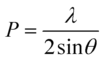
Lloyd's mirror configuration-based laser interference lithography consisting of an expanded continuous wave was used to produce the nanopatterns. A 15 mW He–Cd laser (Kimmon IK-3151-E) at 315 nm wavelength with a Gaussian profile was employed as the illumination source. The substrate and a flat surface aluminium mirror were fixed perpendicular to each other using a V-block. Two exposures separated by a 90-degree rotation of the sample were used to obtain the desired 2D arrays. The nanostructure pitch (P) due to the interference of the laser beams is defined as follows:where λ is the wavelength of the incident beam, θ is the angle between the incident laser and sample normal.
Fabrication process
Silicon substrates were spin-coated with a 60 nm BarLi-II ARC followed by a 150 nm AZ-MiR-701 positive-tone photoresist. The laser power was set at 10 mW and samples were exposed for 90 to 100 s per sample orientation. The dose for each exposure was set such that only doubly exposed regions are above the development threshold. After development, the topmost squaroid posts result from the overlap of regions with destructive interference from the double exposure. The middle layer results from the incomplete destructive interference of the incident waves with its reflection from the substrate, where holes formed in this layer occur where constructive interference forms high intensity regions above and below. The region right below this middle layer receives a higher dose of exposure and thus develops more rapidly, resulting in the overhang structure with fragile resist posts connecting each layer as shown in the tilt-view SEM in Fig. 2. A sample was developed using diluted TMAH solution (1:1 with DI-water) for 15 to 20 s. Finally, a 20 nm layer of aluminum was deposited using an electron-beam evaporator.
Characterization
Scanning electron microscopy (SEM) images were taken with a JEOL JSM 7600F field emission scanning electron microscope with an acceleration voltage of 5 kV. The experimental reflectance spectra were collected with a microspectrometer system (CRAIC QDI2010, CRAIC Technologies) with an aperture of 2 μm.Finite-difference time-domain (FDTD) simulations
FDTD simulation was carried out with commercial software FDTD Solutions (v8.12.527, Lumerical Solutions, Inc.). The simulated structures with different combinations of three layers were constructed based on experimental parameters. Symmetry/anti-symmetry boundary conditions were used on lateral dimensions while at the vertical dimension perfectly-matched layers (PML) were used with the simulation region being 350 nm in both x and y directions and 600 nm away from the top of simulated nanostructures. The mesh size was chosen to be 1 nm along all three dimensions. Mesh accuracy was set to be 3 for accurate and detailed results. The overall structure is illuminated with a normal incident plane wave source. The optical parameters of aluminum were taken from Palik's handbook, and photoresist, BarLi II from supplier's datasheets.Results and discussion
Overview of 3-tiered plasmonic superlattice
In our previous work we have established an approach for realizing plasmonic color mixing by laterally combining different nanostructures into a single color pixel.8 In contrast, the structures here are combined vertically and the properties of the resulting stack are investigated. The 3-tiered partially exfoliated plasmonic color stack is illustrated in Fig. 1. The nanostructure is made up of three layers with distinct geometries vertically separated from each other. By varying the surface geometry in both lateral and vertical dimensions, we achieved distinct plasmonic colors.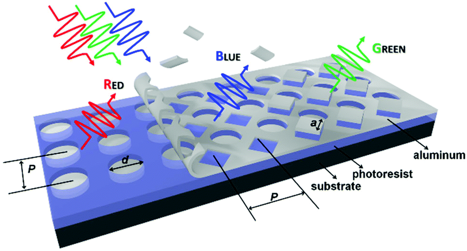 | ||
| Fig. 1 Schematic of the 3-tiered plasmonic superlattice. Metallic nanostructures consisting of 3 layers of nanostructure including: disk array (bottom), nanohole super-array (middle), and squaroid array (top). Peel-off or exfoliation of plasmonic nanostructure layers exposes drastically different colors beneath. Structural parameters of fabricated samples are marked as follows: pitch (P) = 350 nm; diameter (d) of circular disk/hole ranging from 240 to 332 nm; and edge size (a) of square hole/squaroid ranging from 138 to 235 nm. | ||
We first describe one of the constituent layers of the superlattice, i.e. the nanohole super-array. Here we use circular and square nanohole arrays as examples. The nanohole super-array is formed by performing an XOR operation between the two sets of nanohole arrays shifted by a half of a pitch in both x and y. For simplicity, both arrays are on a square lattice with an identical lattice constant of 350 nm in pitch. Structural parameters are marked as P (pitch), d (diameter of circular hole) and a (edge size of square hole). To form the proposed 3-tiered plasmonic superlattice, the 2D plasmonic super-array is further extended by adding an isolated disk and squaroid arrays in the third dimension. With a disk array introduced beneath and a squaroid array on top, we obtain the 3-tiered plasmonic superlattice.
Experimental realization of 3-tiered plasmonic superlattice
Laser interference lithography is versatile in constructing surface nanostructures through altering the constructive/destructive interference patterns in three dimensions. Here we utilize laser interference in lateral and vertical dimensions to form complex nanostructures within a layer of photoresist to create the desired 3D geometries that are sufficiently delicate to enable exfoliation. Fig. 2 shows a process flow to fabricate the 3D plasmonic superlattice via laser interference lithography (LIL) and metal evaporation (details in the Experimental section). A silicon substrate coated with a 150 nm-thick photoresist on a 60 nm anti-reflection coating (ARC) is exposed twice with a He–Cd 315 nm wavelength laser in a Lloyd's mirror setup with the sample rotated by 90 degree between exposures (Fig. 2A). The angle between the incident laser and sample normal was set to 28 degree so as to define the pitch to be 350 nm. The simulated interference pattern due to the double exposure and reflection from the substrate is shown in Fig. 2 (inset). While a ∼200 nm-thick ARC would have completely removed the standing wave in the vertical direction, the 60 nm-thick ARC used produced an optimum standing-wave pattern as shown while acting also as an adhesion promoter for the resist. After development, the resist structure consisting of a square post array on top with circular through-hole arrays at the bottom (Fig. 2B) was constructed. The overall height of the photoresist decreased from 150 nm to 135 nm after development. Finally, a 20 nm-thick aluminum layer was deposited using electron-beam evaporation to provide plasmonic features that form the 3-tiered plasmonic superlattice, as shown in Fig. 2C. Fig. 2E and F shows scanning electron micrograph (SEM) images of the top and tilted views of the structure where the stacked metallic nanostructures can be clearly observed. An illustration of the cross-section profile is depicted in Fig. 2D, indicating that the height of the second layer is 95 nm, as used in the following simulations.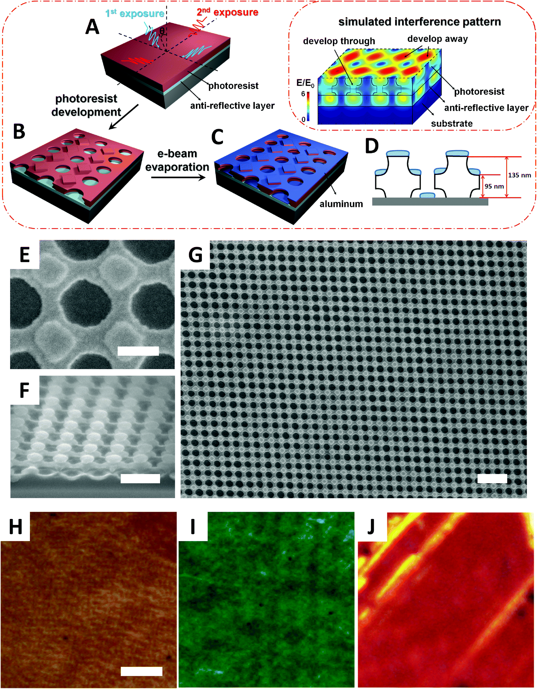 | ||
| Fig. 2 (A–C) Schematic illustration of the fabrication process for the 3-tiered plasmonic superlattice. (A) Double exposure by laser interference lithography. (B) Photoresist development. (C) Electron-beam evaporation of aluminum. (D) Illustrative sketch (not to scale) showing structural parameters along the vertical dimension. Photoresist structure outlined black. 20 nm thick aluminum shown in light blue. (Inset) Simulated exposure intensity plot of the laser interference pattern at 315 nm wavelength. Red regions with higher exposure intensities removed during the resist development process, leaving blue regions to form final 3-tiered structures. (E, F) SEM images of representative plasmonic nanostructures from top view (E) and tilted view (F) at 30 degree. (G) SEM image of large area 3-tiered nanostructures. Scale bars: 200 nm (E), 500 nm (F) and 1 μm (G). (H–J) Optical microscopy images of 3-tiered plasmonic superlattices with structural parameters designed as: d = 220 nm, a = 178 nm (H); d = 250 nm, a = 170 nm (I); and d = 280 nm and 180 nm, a = 200 nm and 100 nm along the long and short axis, respectively (J). Pitch (P) was held at a constant value of 350 nm throughout the experiments. Scale bar: 20 μm. | ||
From the SEM images in Fig. 2E–G, a well-established periodic nanostructure can be clearly observed. Note that the sample was not rotated by exactly 90 degree between exposures, resulting in the skewed grid shown. Top-view SEM images of the 3-tiered nanostructures show distinguished features and the dimensions are consistent with the simulated results (Fig. 2, inset). SEM image at a lower magnification in Fig. 2G indicates the capability of constructing complex 3-tiered nanostructures over large areas with well-defined nanostructures.
The lateral structural parameters of the 3-tiered plasmonic superlattice can be tuned by altering the angle of the incident laser and development conditions, hence achieving a range of colors from the plasmonic color stacks, as shown in Fig. 2H–J. Increasing development time results in a larger hole and smaller squaroid size, as shown in Fig. S1A and S1B.† The change in feature sizes is responsible for the color change from brown to green for a constant 350 nm pitch. Varying the rotation angle between exposures results in elongated structures (see Fig. S1C,† rotation angle: 60 degree), which results in the dark-red color, and polarization-dependent colors (not measured). Tilted-view SEM image in Fig. 2F shows an overhang structure for the top layer, and a second layer that is suspended (with some broken bridges) instead of directly resting on the substrate. These fragile features thus enable the exfoliation of individual structures.
Mechanical exfoliation of layers
To sequentially remove each layer, we used a pair of tweezers and manually made gentle scratches and repeated contact with the surface of the sample. As expected, the process is not yet controllable and results in areas with single, double or damaged layers. We expect to better control this process with the use of adhesive tape or polymeric elastomers such as the polydimethylsiloxane (PDMS) film.Unlike 2D materials where the number of layers is identified by different shades of gray, exfoliating the plasmonic superlattice stack results in obvious color changes, as shown in Fig. 3A–C. The results show that the sample color changes from green → blue → red with the exfoliation of each layer. Regions of incomplete removal of the outer layers are seen in Fig. 3B and C, suggesting that the color change is due to surface reconstruction via removal of plasmonic layers. Corresponding SEM images in Fig. 3D–F show the superlattice structures under the pristine conditions, top square posts removed, with only the bottom disks remaining. Remarkably the exfoliation can neatly remove both the squaroid metal and its supporting resist structures, although residues are seen to increase with the number of layers removed. The disks show a vibrant red color, as they were separated from the Si substrate by the ARC. The SEM image contrast between the metal and photoresist was low due to the low secondary-electron yield when imaging aluminum (a low atomic number metal).
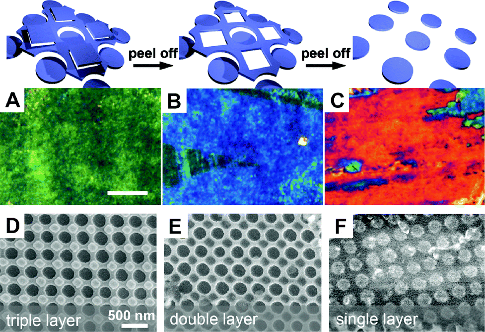 | ||
| Fig. 3 Optical microscopy images of 3D plasmonic superlattice with all three layers (A), two layers (B), and a single layer (C) of metallic nanostructures showing the color change when layers were exfoliated. Scale bar: 10 μm. (Insets) Schematics of the corresponding metal structures (photoresist not shown for clarity). (D, E, F) Corresponding SEM images showing nanostructures with the vertical stacking of layers: (D) triple-layer; (E) double-layer, and (F) single layer. Scale bar: 500 nm. | ||
We note that the adhesion of Al with the resist structures appeared to be good as exfoliation always involved the removal of both Al and the resist structures attached to it. Within reason, we can expect a similar adhesion strength between the Al and the ARC layer, allowing exfoliation to be conducted without removal of the disks attached to the ARC.
While we have yet to develop a procedure to exfoliate layers controllably and sequentially, our observations of the top layer being removed without affecting the middle layer suggests that such a procedure can be conceived. One imagines a careful process where the contact pressure of a soft material, e.g. PDMS, is applied to touch and remove only the topmost layer. The exposed second layer can then be removed easily. Likewise, applying a higher pressure with a softer more conformal adhesive material could allow both layers to be exfoliated in a single step.
Numerical analysis
To address the interactions between the three plasmonic layers fabricated here, we performed finite-difference time-domain (FDTD) numerical simulation to first investigate the optical characteristics of the fundamental layer in the middle, i.e. the nanohole super-array. The aluminum nanohole super-array is supported by a photoresist-coated silicon substrate to match the experiments. The simulated reflectance spectra are shown in Fig. S2† for the values of a/d varying from 0.42 to 0.98, while fixing the width of the metal separating the circular and square hole at 12 nm. Clear spectral shifts and the emergence of multiple resonance modes are observed. At the largest circular hole of 332 nm diameter, the spectrum exhibits a broad dip at 550 nm (green marker). Its corresponding electric-field intensity and charge distributions indicate a dipolar resonance inside the circular and square holes. Increasing the a/d ratio redshifts the resonance mode as indicated by the dashed line from the green marker (dip @514 nm) to the red marker (dip @674 nm). The mode evolves into a hybridized bonding mode between a dipolar resonance of the circular hole and a hexapolar resonance of the square hole. Its hybridized anti-bonding counterpart emerges at ∼500 nm (blue marker) and does not shift with varying a/d ratios. More details on the modes and hybridization between the two sets of hole arrays are presented in Fig. S3–S5.†Having established an understanding of the plasmonic behavior of the nanohole super-array, we further extend the analysis of the nanostructure to three tiers making it possible to compare the theoretical results with the experimental ones. Measured and simulated reflectance spectra of the structures with different numbers of layers are shown in Fig. 4A.
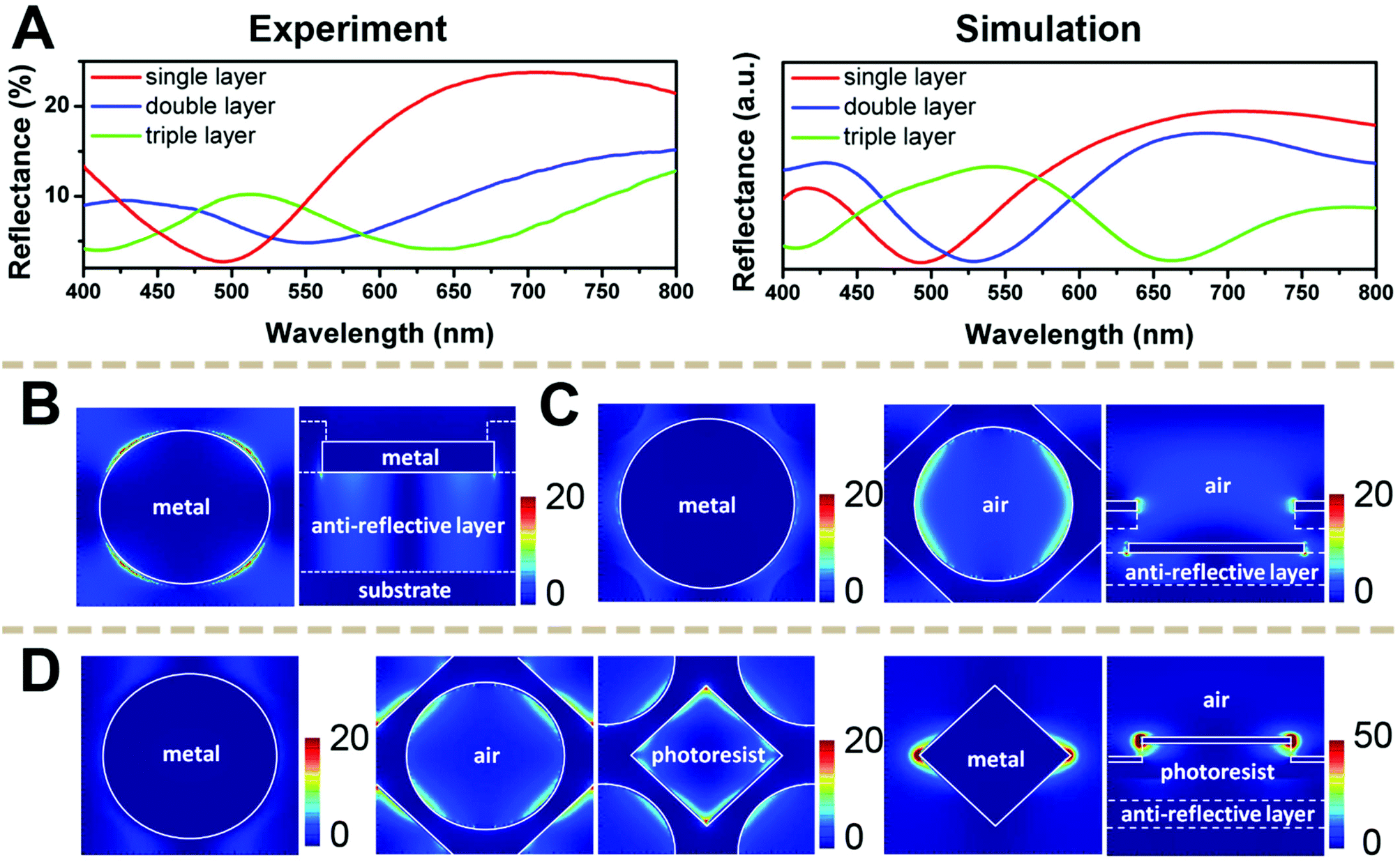 | ||
| Fig. 4 (A) Experimental (left) and simulated (right) reflectance spectra of different layers. (B, C, D) Simulated electric field distribution |E/E0|2 at resonant positions. (B) Single layer @490 nm a circular disk array at the bottom; (C) double layer @528 nm consisting of the bottom disk (left) and super-array in the middle (right); and (D) the full 3-tiered structure @658 nm including (from left to right): a disk array at the bottom; super array in the middle, and a squaroid array at the top. Aluminum structures outlined in solid lines in (B, C, and D), dashed lines outline non-plasmonic components, i.e. the photoresist and ARC layer. | ||
We expect some of the elongated structures as in Fig. S1C† to exhibit dependence on incident light polarization. However, the samples that were investigated through spectrometry and simulations in Fig. 4 were only slightly asymmetric. Thus we do not expect large polarization dependence, and unpolarised light was used for these measurements.
Simulations show a reasonable agreement with the experiments, despite the idealized geometries used. To understand the optical behaviors of the 3D plasmonic superlattice with different layers, we looked at the field distribution at the resonant wavelengths at different cross sections through the structure. The single layer consisting of an aluminum disk array with a diameter of 250 nm and periodicity of 350 nm, shows a clear reflectance dip at ∼490 nm. Calculated electric field distribution shows that this dip is due to the excitation of a high-order quadrupolar resonance. We attribute it to the disk size together with the presence of an asymmetric Fabry–Perot cavity underneath (Fig. 4B). A simple dipole resonance occurs in the infrared region at ∼850 nm (not shown) due to the large disk size.15
As we stack on the middle layer, the spectrum is modified in agreement with the measurements. According to the simulation results from Fig. 4C, the middle layer confines most of the energy in the dipolar resonance of the circular holes. Coupling with the dipolar-like resonance of the bottom disks occurs though the field enhancement is decreased around the disk. Due to the larger size of the circular holes, the square holes from the middle layer do not confine much energy, as shown in Fig. S1.† The coupling between the two layers causes the resonance wavelength to red-shift and produces the observed blue color (Fig. 3B).
For the full 3-tiered superlattice structure, the resonance position is further red-shifted. With normal-incidence illumination, the square structures on the top are excited with a strong dipolar resonance due to the shape effect.20 This mode couples with the middle layer resulting in a more equal field distribution within the square and circular holes. The presence of the top metal layer thus plays a vital role in coupling the electric field from within circular holes to both circular and square holes. In general, we observe that the field intensities are confined to the top-most structures as can be seen in the cross-sectional field distribution plots.
The effect of photoresist removal on color change was minimal. Simulated spectra in Fig. S6† shows that the photoresist structure accounts for only 8 nm shift in the resonance position as the height (h) of the photoresist post was varied from 0 to 30 nm. In contrast, the presence or absence of the metal square accounts for ∼150 nm shift, accounting for the overall color change from green to blue.
Finally, we perform a thorough structural decomposition to show that the coupling of the two top-most plasmonic structures sufficiently determines the color of the entire stack. Fig. 5 shows the simulated reflectance spectra for different combinations of the superlattices. Note that the spectrum for the full 3-tiered structure is close to that with only the top two layers, but different from that with just the top layer. Similarly, with the top layer removed, the middle layer alone is insufficient to determine the spectrum. These results suggest that for a stack consisting of N layers (Nth layer on top), the plasmon coupling between the N and N − 1 layers could sufficiently determine the color of the entire stack. However the plasmon resonance of the Nth layer alone is insufficient.
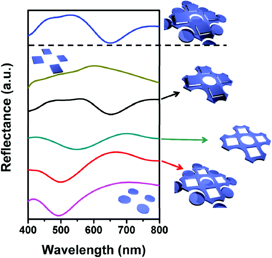 | ||
| Fig. 5 Calculated reflectance spectra of the 3D plasmonic superlattice divided into (from bottom to top): a bottom circular disk layer (magenta line); a double layer with a circular disk and nanohole super-array (red line); a nanohole super-array only (dull green); an upper two-layer consisting of nanohole super-array and a square disk (black line); an upper square disk layer (dull yellow line); and a full 3D plasmonic superlattice structure (blue line). | ||
Conclusions
The concept of 3D plasmonic superlattice colors as introduced here provides a means for color information to be encoded into multiple layers within a sub-wavelength (<200 nm) thickness of materials. A fabrication process was developed to create complex 3D nanostructures. Crucially, the use of laser interference lithography makes it possible to create stacked nanostructures that are weakly connected in the vertical direction. The resulting 3-tiered superlattice structures can thus be sequentially exfoliated leading to a drastic change from green → blue → red. The absorptive nature of the plasmonic structures causes the colors observed to be defined by the hybridized plasmon resonances of the two topmost layers, with a minimal effect from deeper layers. Due to the localized nature of these resonances, the 3D color superlattices can encode diffraction-limited color information, e.g. via controlled milling or removal of the layers, or by laser writing.7 Other practical applications include color changing labels in tamper-evident seals, and or pressure-responsive color surfaces.Competing interest
The authors declare no competing financial interest.Acknowledgements
This work was supported by the SUTD-MIT International Design Centre (IDC) Grant No. IDG31400113, SUTD Digital Manufacturing and Design Centre (DmanD) Grant No. RGDM 1530302, SUTD Startup Research Grant No. SREP13069, and A*STAR, SERC 2014 Public Sector Research Funding (PSF) Grant: SERC Project No. 1421200080.Notes and references
- N. J. Halas, S. Lal, W.-S. Chang, S. Link and P. Nordlander, Chem. Rev., 2011, 111, 3913–3961 CrossRef CAS PubMed.
- Y. Gu, L. Zhang, J. K. W. Yang, S. P. Yeo and C.-W. Qiu, Nanoscale, 2015, 7, 6409–6419 RSC.
- E. C. Dreaden, A. M. Alkilany, X. Huang, C. J. Murphy and M. A. El-Sayed, Chem. Soc. Rev., 2012, 41, 2740–2779 RSC.
- G. Si, Y. Zhao, J. Lv, M. Lu, F. Wang, H. Liu, N. Xiang, T. J. Huang, A. J. Danner, J. Teng and Y. J. Liu, Nanoscale, 2013, 5, 6243–6248 RSC.
- J. Olson, A. Manjavacas, L. Liu, W.-S. Chang, B. Foerster, N. S. King, M. W. Knight, P. Nordlander, N. J. Halas and S. Link, Proc. Natl. Acad. Sci. U. S. A., 2014, 111, 14348–14353 CrossRef CAS PubMed.
- J. Xue, Z.-K. Zhou, Z. Wei, R. Su, J. Lai, J. Li, C. Li, T. Zhang and X.-H. Wang, Nat. Commun., 2015, 6, 8906 CrossRef CAS PubMed.
- X. Zhu, C. Vannahme, E. Højlund-Nielsen, N. A. Mortensen and A. Kristensen, Nat. Nanotechnol., 2015, 11, 325–329 CrossRef PubMed.
- S. J. Tan, L. Zhang, D. Zhu, X. M. Goh, Y. M. Wang, K. Kumar, C.-W. Qiu and J. K. W. Yang, Nano Lett., 2014, 14, 4023–4029 CrossRef CAS PubMed.
- X. M. Goh, Y. Zheng, S. J. Tan, L. Zhang, K. Kumar, C.-W. Qiu and J. K. W. Yang, Nat. Commun., 2014, 5, 5361 CrossRef CAS PubMed.
- H. Duan, H. Hu, K. Kumar, Z. Shen and J. K. W. Yang, ACS Nano, 2011, 5, 7593–7600 CrossRef CAS PubMed.
- A. Joshi-Imre and S. Bauerdick, J. Nanotechnol., 2014, 2014 Search PubMed.
- F. Watt, A. A. Bettiol, J. A. Van Kan, E. J. Teo and M. B. H. Breese, Int. J. Nanosci., 2005, 04, 269–286 CrossRef CAS.
- N. Vogel, M. Retsch, C.-A. Fustin, A. Del Campo and U. Jonas, Chem. Rev., 2015, 115, 6265–6311 CrossRef CAS PubMed.
- B. Ai, Y. Yu, H. Möhwald and G. Zhang, Adv. Opt. Mater., 2013, 1, 724–731 CrossRef.
- L. Wang, R. J. H. Ng, S. Safari Dinachali, M. Jalali, Y. Yu and J. K. W. Yang, ACS Photonics, 2016, 3, 627–633 CrossRef CAS.
- P. Zijlstra, J. W. M. Chon and M. Gu, Nature, 2009, 459, 410–413 CrossRef CAS PubMed.
- H. Wolferen, L. Abelmann and H. van Wolferen, in Lithography: Principles, Processes and Materials, ed. T. C. Hennessy, Nova Science Publishers, Hauppauge NY, 2011, ch. 5, pp. 133–148 Search PubMed.
- Y. Shen, J. Zhou, T. Liu, Y. Tao, R. Jiang, M. Liu, G. Xiao, J. Zhu, Z.-K. Zhou, X. Wang, C. Jin and J. Wang, Nat. Commun., 2013, 4, 2381 Search PubMed.
- E. Prodan, C. Radloff, N. J. Halas and P. Nordlander, Science, 2003, 302, 419–422 CrossRef CAS PubMed.
- A. Agrawal, I. Kriegel and D. J. Milliron, J. Phys. Chem. C, 2015, 119, 6227–6238 CAS.
Footnotes |
| † Electronic supplementary information (ESI) available. See DOI: 10.1039/c6nr03466g |
| ‡ These authors contributed equally to this work. |
| This journal is © The Royal Society of Chemistry 2016 |