
 Open Access Article
 This Open Access Article is licensed under a Creative Commons Attribution-Non Commercial 3.0 Unported Licence
Spun-wrapped aligned nanofiber (SWAN) lithography for fabrication of micro/nano-structures on 3D objects†
Zhou
Ye
a,
Amrinder S.
Nain
abc and
Bahareh
Behkam
*abc
aDepartment of Mechanical Engineering, Virginia Tech, Blacksburg, VA 24061, USA
bSchool of Biomedical Engineering & Sciences, Virginia Tech, Blacksburg, VA 24061, USA
cMacromolecules Innovation Institute, Virginia Tech, Blacksburg, VA 24061, USA. E-mail: behkam@vt.edu
First published on 1st June 2016
Abstract
Fabrication of micro/nano-structures on irregularly shaped substrates and three-dimensional (3D) objects is of significant interest in diverse technological fields. However, it remains a formidable challenge thwarted by limited adaptability of the state-of-the-art nanolithography techniques for nanofabrication on non-planar surfaces. In this work, we introduce Spun-Wrapped Aligned Nanofiber (SWAN) lithography, a versatile, scalable, and cost-effective technique for fabrication of multiscale (nano to microscale) structures on 3D objects without restriction on substrate material and geometry. SWAN lithography combines precise deposition of polymeric nanofiber masks, in aligned single or multilayer configurations, with well-controlled solvent vapor treatment and etching processes to enable high throughput (>10−7 m2 s−1) and large-area fabrication of sub-50 nm to several micron features with high pattern fidelity. Using this technique, we demonstrate whole-surface nanopatterning of bulk and thin film surfaces of cubes, cylinders, and hyperbola-shaped objects that would be difficult, if not impossible to achieve with existing methods. We demonstrate that the fabricated feature size (b) scales with the fiber mask diameter (D) as b1.5 ∝ D. This scaling law is in excellent agreement with theoretical predictions using the Johnson, Kendall, and Roberts (JKR) contact theory, thus providing a rational design framework for fabrication of systems and devices that require precisely designed multiscale features.
Introduction
High-throughput, scalable, and cost-effective fabrication of micro/nano-structures on three-dimensional (3D) objects is crucial for the development of new paradigms in diverse fields including metamaterials,1 optoelectronics,2 nanophotonics and plasmonics,3,4 biosensing,5,6 lab-on-fiber technologies,7 energy harvesting and storage.8 There is also a great need for fabricating nanostructures on the surface of biomedical devices and implants where micro/nanoscale surface features have been shown to promote tissue regeneration9 and inhibit microbial fouling.10 As such, numerous attempts have been made to develop new techniques11–14 and also adapt the conventional nanofabrication techniques such as electron beam lithography (EBL)15,16 and soft lithography11,12,17–22 for nanofabrication on non-planar surfaces. Despite the many positive attributes of these techniques, the high sensitivity of pattern fidelity to overall 3D object shape and limitations with respect to throughput, scalability, reliability, affordability, and substrate material compatibility present significant barriers to their use for nanopatterning of large-areas of pre-structured 3D objects. Presently, to the best of our knowledge, there is no method capable of whole surface nanopatterning of irregularly shaped or highly non-planar 3D objects. Furthermore, simultaneous fabrication of multiscale (i.e. micro- and nanoscale) structures on 3D substrates remains a formidable challenge thwarted by limited affordability and scalability of the aforementioned state-of-the-art techniques. Thus, there is a compelling need to develop new nanoscale as well as multiscale fabrication technologies.Here, we report a versatile and scalable technique, termed Spun-Wrapped Aligned Nanofiber (SWAN) lithography, for fabrication of multiscale structures on large areas of planar and non-planar substrates without a master and at high-throughput in standard laboratory setting. The process flow of SWAN lithography is illustrated in Fig. 1. In the first step, the non-electrospinning Spinneret-based Tunable Engineered Parameters (STEP) technique23,24 was used to deposit polystyrene (PS) fibers with precisely controlled diameter, spacing and orientation onto a 3D substrate. The nanofiber mask is deposited in an array of uniform diameter fibers at a constant or a prescribed varying spacing. Multiple arrays each with different diameter and spacing may be deposited in one layer or in a 3D multi-layer configuration (Fig. 1a). In the second step, the fiber-masked substrate was placed under vacuum in an enclosure containing tetrahydrofuran (THF, a good PS solvent) vapor to carry out a controlled fiber deformation process and achieve the desired fiber-substrate contact area. In the third step, the substrate was etched to transfer the fiber mask pattern onto the substrate. In the final step, the PS fiber mask was dissolved. SWAN lithography is applicable to both bulk and thin film patterning; thus enabling incorporation of passive (e.g. nanostructures for controlling cell behavior on implants) or functional devices (e.g. electronic circuits for sensing) onto curved surfaces and 3D objects.
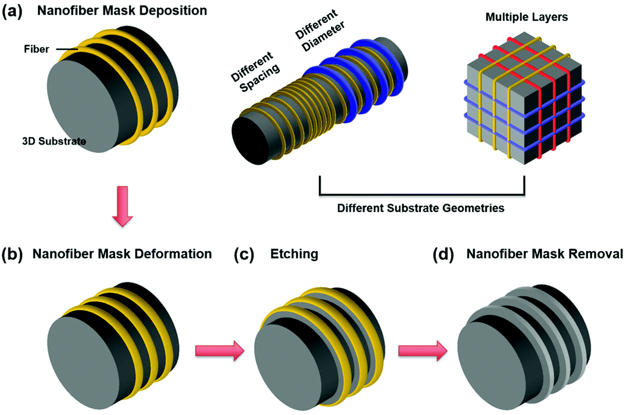 | ||
| Fig. 1 Schematic illustration of SWAN lithography. (a) High throughput continuous deposition of PS fibers on a 3D substrate using the STEP technique. Fiber mask arrays can be deposited in single or multiple layers of the same or different diameter and spacing. (b) Exposure of the fiber-masked substrate to the solvent vapor for controlled deformation of the fiber mask. (c) Etching of the fiber-masked substrate to create micro/nanostructures. (d) Removal of the fiber mask in PS solvent. | ||
Experimental section
Nanopatterning of glassy carbon (GC) substrates
All experiments were performed at room temperature unless otherwise stated. A total of six PS solutions were prepared by dissolving PS (Scientific Polymer Products) in xylene (Fisher Scientific) at 10 wt% for PS of 860 kg mol−1 molecular weight, and at 5 wt%, 7 wt%, 10 wt%, 14 wt%, and 18 wt% for PS of 2000 kg mol−1 molecular weight. Fiber arrays were deposited on GC SIGARADUR® (Hochtemperatur-Werkstoffe GmbH, Germany) plates (10 mm × 10 mm × 1 mm), cylinders (Ø 3 mm × 5 mm), and cubes (6 mm × 6 mm × 6 mm) using the STEP technique.24 Briefly, PS solution was pumped through a glass micropipette to form an extruded droplet at the pipette tip. The droplet was brought into contact with the substrate to form a fiber, and aligned fibers were continuously wrapped around the rotating substrate. The substrate was moved using a 3D motorized stage to form the fiber mask pattern with controlled fiber spacing. The fiber-masked substrate was placed in an enclosure containing THF under a vacuum pressure of −0.68 bar. After exposure to THF vapor for the specified duration, the sample was electrochemically etched at 2.0 V (vs. Ag/AgCl) in 0.1 M NaOH solution with platinum gauze connected to a platinum wire as the counter electrode.25 After etching, PS fibers were dissolved in methylene chloride, and GC substrate was treated in piranha solution (3![[thin space (1/6-em)]](https://www.rsc.org/images/entities/char_2009.gif) :1 H2SO4 and H2O2) for 30 min to remove the PS residue. After each use, the GC plates were serially polished by 1 μm, 0.3 μm, and 0.05 μm alumina slurry (Electron Microscopy Sciences) to remove etched features for the subsequent set of experiments. The scratches appearing in some of the SEM and AFM images (Fig. 5 and 6) were from polishing. After polishing, the resulting surface roughness was 5.1 ± 0.4 nm.
:1 H2SO4 and H2O2) for 30 min to remove the PS residue. After each use, the GC plates were serially polished by 1 μm, 0.3 μm, and 0.05 μm alumina slurry (Electron Microscopy Sciences) to remove etched features for the subsequent set of experiments. The scratches appearing in some of the SEM and AFM images (Fig. 5 and 6) were from polishing. After polishing, the resulting surface roughness was 5.1 ± 0.4 nm.
Nanopatterning of gold film
A borosilicate glass rod (Ø 5 mm) was pulled to a hyperbola shape on an open flame. The hyperbola-shaped glass was cleaned in piranha solution for 30 min, followed by rinsing with deionized water and flushing with dry air. The glass sample was further dried at 180 °C for 30 min. A thin Ti (adhesion promoter) and Au film were sequentially deposited onto the glass sample by electron beam evaporation (Kurt J. Lesker PVD-250). To achieve uniform evaporated gold thickness, the glass substrate was continuously rotated along its axis during the deposition process. A PS fiber array was deposited onto the gold surface and heated in an oven at 110 °C for 20 min to increase adhesion. Then, the fiber-masked sample was etched in freshly prepared gold etchant (15 mM thiourea, 10 mM Fe(NO)3, 1.2% HCl)26 for 2 min while stirring at 350 rpm. PS fibers were dissolved in methylene chloride after etching, leaving behind the metallic features.Surface characterization
Lateral dimensions and heights of the nanopatterned features were measured using scanning electron microscopy (SEM) and atomic force microscopy (AFM), respectively. SEM imaging obtained at an electron beam energy of 5 keV were used to measure fiber diameter and etched feature widths. To measure the height of the etched features, AFM scanning was performed with a Si probe (NANOWORLD NCST-20) in tapping mode. All experimental data was obtained from at least two independent sets of experiments with multiple measurements (at least 10 per sample) on multiple samples to verify the repeatability.Results and discussion
We demonstrate the versatility of SWAN lithography in patterning of 3D objects with various degrees of non-planarity, followed by detailed characterization of the SWAN lithography process itself. SWAN lithography enables simultaneous nanopatterning of the full arc length of curved geometries, such as the GC cylinder (Ø 3 mm × 5 mm) shown in Fig. 2a. PS fiber masks of different diameters resulted in multiscale etched features with widths of 900 nm, 50 nm, or alternating width of 50 nm and 150 nm that were formed on the entire lateral surface of the cylinder with high pattern fidelity. Such nanopatterned substrates may be utilized as highly sensitive neural electrodes.27 A GC cube (6 mm × 6 mm × 6 mm) was modified by polishing one of its vertices to create a triangular face on the vertex (Fig. 2b). Separate layers of PS fibers, each with a different diameter, were deposited in three different orientations that crossed at 60° angles. Solvent vapor treatment and electrochemical etching resulted in 300 nm, 600 nm, and 900 nm wide etched features on the vertex surface (Fig. 2b-i). Similarly, 350 nm wide etched features in a crisscross pattern were achieved on the lateral surfaces of the GC cube (Fig. 2b-ii). Pattern fidelity across adjoining faces and at sharp corners can be robustly achieved, as shown in Fig. 2b-iii. Such 3D objects covered with nanostructures on all surfaces constitute a new class of passive devices which for example can be utilized in antireflectivity applications.28 | ||
| Fig. 2 Fabrication of micro/nano-structures on non-planar GC surfaces. (a) Multiscale structures on the lateral surface of a GC cylinder. SEM images show linear features with widths of (a-i) 900 nm, (a-ii) 50 nm, or (a-iii) alternating widths of 50 nm and 150 nm. (b) Patterning of a GC cube with a polished vertex. SEM image of (b-i) crisscross linear features with three different widths of 300 nm, 600 nm, and 900 nm on the polished vertex of the GC cube, (b-ii) 350 nm wide etched features in an electronic circuit pattern on a face of the GC cube, (b-iii) the etched features along an edge of the GC cube. | ||
For many functional device applications, it is desirable to pattern a deposited metal film. As a proof of concept, we deposited a thin film of gold on a hyperbola-shaped glass substrate (Fig. 3a), followed by deposition of the PS nanofiber mask and wet etching to achieve 300 nm wide gold features over the entire surface of the object. The variation in cross-sectional area and curvature of the substrate had no impact on uniformity of the nanopatterns (Fig. 3b), which in comparison is difficult to achieve by EBL or soft lithography. The gold patterns formed may be used as components of electrical or optical devices or as resists for further processing of the underlying substrate to achieve high aspect ratio features. This process may also be used to pattern optical fibers for a host of imaging and sensing applications.29
 | ||
| Fig. 3 Patterned gold film on a hyperbola-shaped glass substrate. (a) Photograph of the original (left) and the nanostructured (right) substrates with structural coloration. SEM image shows 300 nm wide gold lines on the lateral surface with changing curvature. (b) Curvature change along the length of the substrate. SEM images are from the marked locations with different curvatures. All scale bars are 10 μm. | ||
Next, we characterized the SWAN lithography process on flat GC substrates (10 mm × 10 mm × 1 mm). Features of different sizes were obtained by either controlling the diameter of fibers23,24 or by controlling the size of the fiber-substrate contact area (Fig. 4 and 5). To investigate the dependency of the etched feature width upon fiber diameter, fibers of various diameters were deposited on flat GC substrates. All samples were exposed to THF vapor for 3 min to enhance interfacial adhesion without changing the fiber morphology and were then etched for a short period of time (5 s). The etched feature widths were equal to the fiber-substrate contact widths and were measured to be (fiber diameter: etched feature size (mean ± s.d.)) 85 ± 6 nm: 46 ± 3 nm, 134 ± 8 nm: 82 ± 7 nm, 173 ± 9 nm: 111 ± 7 nm, 219 ± 15 nm: 141 ± 10 nm, and 374 ± 41 nm: 200 ± 18 nm (Fig. 4a). The fiber diameter-etched feature width relation is in agreement with the Johnson, Kendall, and Roberts (JKR) contact theory,30–32 which states that for a fixed set of materials (PS fiber and GC surface), the contact width (b) scales with the fiber diameter (D) according to b1.5 ∝ D (see Fig. 4 inset). This experimentally validated relationship combined with our ability to deposit fibers of various diameters, offer novel enabling means for single-step fabrication of systems and devices with precisely designed application specific multiscale features.
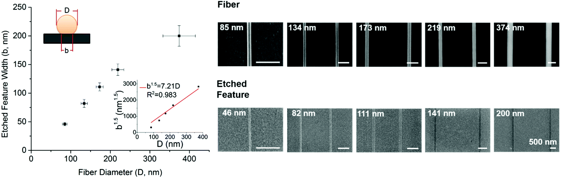 | ||
| Fig. 4 Relationship between the deposited fiber diameter and the etched feature width (n = 573 for fiber diameter measurement, n = 335 for etched feature width measurement). Cartoon shows the cross-section of a fiber deposited on a substrate. SEM images depict fibers with different diameters and the corresponding etched features. The inset plot shows the fitting of experimental data according to the JKR contact theory. All error bars are standard deviations. All scale bars are 500 nm. | ||
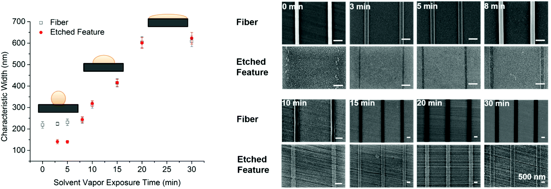 | ||
| Fig. 5 Changing the solvent vapor exposure time to change the etched feature width (n = 867 for fiber width measurement, n = 602 for etched feature width measurement). Cartoons show the deformation of fiber in presence of the solvent vapor. SEM images are fibers and corresponding etched features after different solvent vapor exposure times. All error bars are standard deviations. All scale bars are 500 nm. | ||
While etched feature size can be controlled by fiber diameter, a wider range of feature sizes can be achieved by changing fiber morphology using a controlled solvent vapor treatment process. Solvent molecules penetrate the polymeric fibers, causing them to deform and spread on the substrate.33 Therefore, increasing solvent vapor exposure time can increase the fiber-substrate contact width (Fig. 5). To determine the role of solvent vapor exposure time on feature width, we fixed the PS fiber diameter (219 nm) and varied the solvent exposure duration from 0–30 min. For short 0–3 min exposure duration, fiber contact with the substrate was sporadic, resulting in inconsistencies in feature width. For increased 3–5 min exposure duration, the fiber-substrate interfacial adhesion was enhanced without changing the fiber morphology; thus, the width of the resulting feature remained constant. With further increase in exposure duration (8–20 min), both the fiber contact width and etched feature size were observed to continuously increase. For exposure duration longer than 20 min, no further increase in fiber width was achieved; consequently the etched feature size remained constant. Thus, by exposing 219 nm diameter fibers to THF vapor for 3–30 min, we were able to control etched feature width in the wide range of 141 ± 10 nm to 623 ± 27 nm.
Lastly, the height of the etched features was controlled by varying the duration of the electrochemical etching process. For the fixed process parameters of PS fiber diameter (219 nm) and THF vapor treatment time (20 min with resulting mask contact width of 600 nm), when the etch time was varied from 5 s to 180 s, etched feature height increased from 27 ± 3 nm to 182 ± 18 nm. For etch times longer than 180 s, no further increase in the etched feature height was observed (Fig. 6). This is attributed to the reduction and eventual loss of contact between the fiber and the substrate due to undercutting during the etching process.
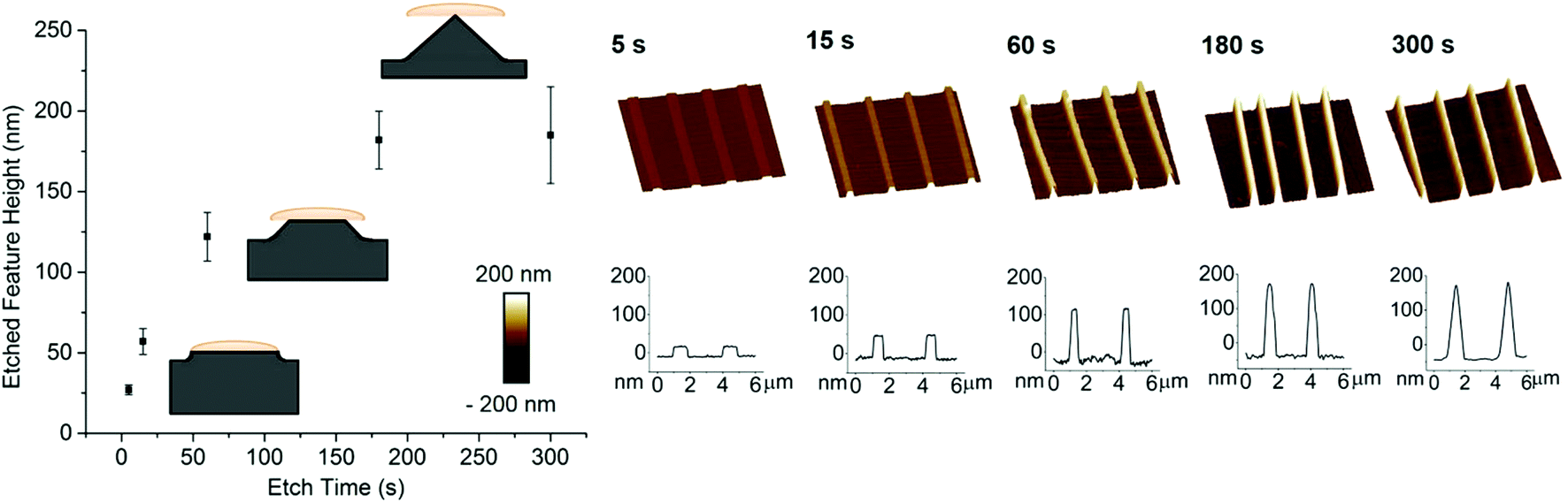 | ||
| Fig. 6 Relationship between etch time and feature height for a fixed feature base width (n = 672). Cartoons show the increasing etched feature heights for longer etch time. AFM cross-section and 3D images show the feature heights for different etch times. All error bars are standard deviations. | ||
SWAN lithography can be applied to other bulk materials (e.g. Si, Fig. S1†) and thin films that can be etched using electrochemical, wet chemical, or dry etching processes. SWAN lithography is also applicable to soft and flexible substrates, such as the commonly used polydimethylsiloxane (PDMS) which can be etched using the reactive ion etching (RIE) technique.34,35 SWAN lithography may be carried out in standard laboratory settings with minimal processing steps and is independent of substrate electrical, optical, or mechanical properties. Size of the fabricated feature is determined by the (1) fiber diameter, (2) fiber and substrate materials, (3) solvent vapor exposure duration, and (4) etching method and duration. Our multiscale lithography method enables high throughput (>10−7 m2 s−1) and large area fabrication of sub-50 nm to several-micron features (Fig. S2†) with exquisite control on feature sizes and high pattern fidelity irrespective of the substrate geometry. Our nanofiber mask deposition method is highly scalable, cost-effective, and is capable of achieving even higher throughputs (Fig. S3†).
The distinguishing features of the SWAN lithography, compared to other methods that are also based on direct deposition of masking geometries,36,37 are: (i) defect-free patterning over large-areas, (ii) multiscale patterning in a single step, (iii) wrapping of the masking geometry around the object which enables whole surface nanopatterning of macroscale objects in a single step. SWAN lithography also offers distinct advantages in comparison with the conventional nanofabrication techniques of EBL, soft lithography, and direct-write methods. In contrast to EBL, SWAN lithography produces high fidelity patterns over large-areas irrespective of degree of non-planarity of the substrate and overcomes EBL's limitations in the size of the patterned area and achievable resolution that are attributed to variation in beam incidence angle, exposure dosage, and uniformity of resist coating thickness.15,16 In comparison with soft lithography and nanoimprint lithography based techniques,11,12,17–19 SWAN lithography obviates the need for master templates that are typically fabricated using low throughput and costly methods. Furthermore, it overcomes soft lithography's challenge with pattern distortion on highly non-planar or irregularly shaped pre-structured 3D objects, which is shown to occur due to lack of full conformity of the 2D elastomeric stamp17–19 and nanopatterned polymeric device layers.20–22 Our masterless technique can robustly achieve sub-100 nm feature sizes, whereas in soft lithography, low elastic modulus of the stamps makes it highly challenging to reliably achieve sub-100 nm features over large-area 3D objects. Lastly, compared with resistless nanolithography and direct-write methods such as focused ion beam milling and ion beam proximity printing19 that provide more versatility in substrate shape, SWAN lithography has much higher throughput, lower cost, and does not alter the material surface properties.
Conclusions
In conclusion, for the first time, we report a lithography technique for fabrication of multiscale structures, from micro to nanoscale, on the whole surface of pre-structured 3D objects. SWAN lithography enables simple, rapid and affordable production of design iterations of nanopatterned templates (Fig. S4†) and may be utilized to alleviate the main challenge associated with high throughput methods such as soft-lithography and roll-to-roll lithography38 that rely on nanopatterned hard templates. Facile, scalable, cost-effective, and high throughput fabrication of micro/nanostructures on wide variety of 3D substrate geometries provides opportunities in development of new nanodevice configurations that have been difficult or impossible to obtain. Thus, it could significantly contribute to the scientific progress as well as technological advancement in different fields including photonics/plasmonics, electronics, and biotechnology in which unique properties of well-ordered nanoscale patterns enhance functionality and performance.Acknowledgements
This work was partially supported by the Institute for Critical Technology and Applied Science (ICTAS) at Virginia Tech. Z. Y. acknowledges financial support from the Robert E. Hord, Jr. Mechanical Engineering Graduate Fellowship. We would also like to thank M. Ellis for potentiostat instrument access and our MicroN BASE Laboratory colleagues A. Kim, J. Clark, L. Carrasco, E. Leaman, and C. Damico for their help with preliminary experiments and insightful discussions. We thank Z. Morrow and P. Sharma for assistance with photography.References
- V. M. Shalaev, Nat. Photonics, 2007, 1, 41–48 CrossRef CAS.
- X. Wang, C. J. Summers and Z. L. Wang, Nano Lett., 2004, 4, 423–426 CrossRef CAS PubMed.
- N. J. Halas, S. Lal, W.-S. Chang, S. Link and P. Nordlander, Chem. Rev., 2011, 111, 3913–3961 CrossRef CAS PubMed.
- F. Priolo, T. Gregorkiewicz, M. Galli and T. F. Krauss, Nat. Nanotechnol., 2014, 9, 19–32 CrossRef CAS PubMed.
- J. Das and S. O. Kelley, Anal. Chem., 2013, 85, 7333–7338 CrossRef CAS PubMed.
- W. Zhang, K. Patel, A. Schexnider, S. Banu and A. D. Radadia, ACS Nano, 2014, 8, 1419–1428 CrossRef CAS PubMed.
- M. Pisco, F. Galeotti, G. Quero, A. Iadicicco, M. Giordano and A. Cusano, ACS Photonics, 2014, 1, 917–927 CrossRef CAS.
- A. S. Aricò, P. Bruce, B. Scrosati, J.-M. Tarascon and W. van Schalkwijk, Nat. Mater., 2005, 4, 366–377 CrossRef PubMed.
- D. G. Castner and B. D. Ratner, Surf. Sci., 2002, 500, 28–60 CrossRef CAS.
- M. Kargar, J. Wang, A. S. Nain and B. Behkam, Soft Matter, 2012, 8, 10254–10259 RSC.
- E. J. Smythe, M. D. Dickey, G. M. Whitesides and F. Capasso, ACS Nano, 2009, 3, 59–65 CrossRef CAS PubMed.
- D. J. Lipomi, R. V. Martinez, M. A. Kats, S. H. Kang, P. Kim, J. Aizenberg, F. Capasso and G. M. Whitesides, Nano Lett., 2011, 11, 632–636 CrossRef CAS PubMed.
- S. Aksu, M. Huang, A. Artar, A. A. Yanik, S. Selvarasah, M. R. Dokmeci and H. Altug, Adv. Mater., 2011, 23, 4422–4430 CrossRef CAS PubMed.
- D. Chanda, K. Shigeta, S. Gupta, T. Cain, A. Carlson, A. Mihi, A. J. Baca, G. R. Bogart, P. Braun and J. A. Rogers, Nat. Nanotechnol., 2011, 6, 402–407 CrossRef CAS PubMed.
- J. Zhang, C. Con and B. Cui, ACS Nano, 2014, 8, 3483–3489 CrossRef CAS PubMed.
- A. Han, A. Kuan, J. Golovchenko and D. Branton, Nano Lett., 2012, 12, 1018–1021 CrossRef CAS PubMed.
- K. E. Paul, M. Prentiss and G. M. Whitesides, Adv. Funct. Mater., 2003, 13, 259–263 CrossRef CAS.
- B. Farshchian, A. Amirsadeghi, S. M. Hurst, J. Wu, J. Lee and S. Park, Microelectron. Eng., 2011, 88, 3287–3292 CrossRef CAS.
- P. Ruchhoeft, M. Colburn, B. Choi, H. Nounu, S. Johnson, T. Bailey, S. Damle, M. Stewart, J. Ekerdt, S. V. Sreenivasan, J. C. Wolfe and C. G. Willson, J. Vac. Sci. Technol., B, 1999, 17, 2965–2969 CAS.
- W. R. Childs and R. G. Nuzzo, Adv. Mater., 2004, 16, 1323–1327 CrossRef CAS.
- W. M. Choi and O. O. Park, Nanotechnology, 2004, 15, 1767–1770 CrossRef CAS.
- Z. Li, Y. Gu, L. Wangs, H. Ge, W. Wu, Q. Xia, C. Yuan, Y. Chen, B. Cui and R. S. Williams, Nano Lett., 2009, 9, 2306–2310 CrossRef CAS PubMed.
- A. S. Nain and J. Wang, Polym. J., 2013, 45, 1–6 CrossRef.
- A. S. Nain, M. Sitti, A. Jacobson, T. Kowalewski and C. Amon, Macromol. Rapid Commun., 2009, 30, 1406–1412 CrossRef CAS PubMed.
- G. K. Kiema, S. Ssenyange and M. T. McDermott, J. Electrochem. Soc., 2004, 151, C142–C148 CrossRef CAS.
- X. Duan, Y. Zhao, A. Perl, E. Berenschot, D. N. Reinhoudt and J. Huskens, Adv. Mater., 2009, 21, 2798–2802 CrossRef CAS.
- J. Van Dersarl, A. Mercanzini and P. Renaud, Adv. Funct. Mater., 2015, 25, 78–84 CrossRef CAS.
- L. Yao and J. He, Prog. Mater. Sci., 2014, 61, 94–143 CrossRef.
- M. H. Tu, T. Sun and K. T. V. Grattan, Sens. Actuators, B, 2014, 191, 37–44 CrossRef CAS.
- M. Barquins, J. Adhes., 1988, 26, 1–12 CrossRef CAS.
- M. K. Chaudhury, T. Weaver, C. Y. Hui and E. J. Kramer, J. Appl. Phys., 1996, 80, 30 CrossRef CAS.
- K. L. Johnson, K. Kendall and A. D. Roberts, Proc. R. Soc. London, Ser. A, 1971, 324, 301–313 CrossRef CAS.
- B. A. Miller-Chou and J. L. Koenig, Prog. Polym. Sci., 2003, 28, 1223–1270 CrossRef CAS.
- W. Chen, R. H. W. Lam and J. Fu, Lab Chip, 2012, 12, 391–395 RSC.
- J. Garra, T. Long, J. Currie, T. Schneider, R. White and M. Paranjape, J. Vac. Sci. Technol., A, 2002, 20, 975 CAS.
- S.-Y. Min, T.-S. Kim, B. J. Kim, H. Cho, Y.-Y. Noh, H. Yang, J. H. Cho and T.-W. Lee, Nat. Commun., 2013, 4, 1773 CrossRef PubMed.
- S. P. Bhawalkar, J. Qian, M. C. Heiber and L. Jia, Langmuir, 2010, 26, 16662–16666 CrossRef CAS PubMed.
- S. H. Ahn and L. J. Guo, Adv. Mater., 2008, 20, 2044–2049 CrossRef CAS.
Footnote |
| † Electronic supplementary information (ESI) available: SWAN lithography on silicon; comparison of SWAN lithography and state-of-the-art nanopatterning methods; replica molding using SWAN lithography fabricated template; PDMS nanofluidic device, gold nanopattern characterization. See DOI: 10.1039/c6nr03323g |
| This journal is © The Royal Society of Chemistry 2016 |