Lithography-free plasma-induced patterned growth of MoS2 and its heterojunction with graphene†
Abstract
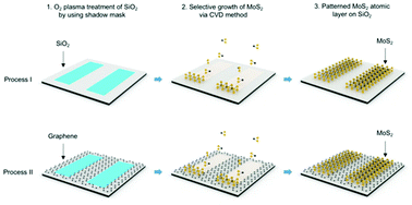
Application-oriented patterned growth of transition metal dichalcogenides (TMDCs) and their heterojunctions is of critical importance for sophisticated, customized two-dimensional (2D) electronic and optoelectronic devices; however, it is still difficult to fabricate these patterns in a simple, clean, and high controllability manner without using optical lithography. Here, we report the direct synthesis of patterned MoS2 and graphene–MoS2 heterojunctions via selective plasma treatment of a SiO2/Si substrate and chemical vapor deposition of MoS2. This method has multiple merits, such as simple steps, a short operating time, easily isolated MoS2 layers with clean surfaces and controllable locations, shapes, sizes and thicknesses, which enable their integration into the device structure without using a photoresist. In addition, we demonstrate the direct growth of patterned graphene–MoS2 heterojunctions for the fabrication of transistor. This study reveals a novel method to fabricate and use patterned MoS2 and graphene–MoS2 heterojunctions, which could be generalized to the rational design of other 2D materials, heterojunctions and devices in the future.
 Please wait while we load your content...

