
 Open Access Article
 This Open Access Article is licensed under a
 Creative Commons Attribution 3.0 Unported Licence
ZnO nanowire array growth on precisely controlled patterns of inkjet-printed zinc acetate at low-temperatures†
Constantinos P.
Tsangarides
,
Hanbin
Ma
 and
Arokia
Nathan
*
and
Arokia
Nathan
*
Electrical Engineering Division, Department of Engineering, University of Cambridge, Cambridge, CB3 0FA, UK. E-mail: ct436@cam.ac.uk
First published on 13th May 2016
Abstract
ZnO nanowires have been fabricated through the hydrothermal method on inkjet-printed patterns of zinc acetate dihydrate. The silicon substrate used was heated accordingly during the printing period in order to maintain good spatial uniformity of the zinc acetate nanoparticles, responsible for the pattern morphology. Printing more than one pass of precursor ink leads to an increase in seed layer thickness that subsequently alters the density and dimensions of nanowires. It has been demonstrated that with the right inkjet-printing parameters and substrate temperature, ZnO nanowires can be effortlessly fabricated in accordance with the desired pattern variations under low temperature and mild conditions that ensures promising applications in optoelectronic devices.
1 Introduction
Zinc oxide (ZnO) is a semiconductor material with a wide direct band gap of 3.37 eV. It is very cheap, abundant and non-toxic with interesting opto-electronic properties which allow it to be used in transparent electrodes,1 thin film transistors,2 chemical or UV sensors,3 light-emitting diodes4 and energy harvesting devices.5 It can be implemented in the form of thin films or nanostructures with the latter being extensively studied.In terms of growing nanostructures like nanowires and nanotubes, various synthesis methods can be employed including the vapour–liquid–solid (VLS) method,6 thermal evaporation,7 chemical-vapour deposition8 and laser ablation.9 These procedures, however, require either high temperatures or expensive equipment. This results in many limitations ranging from limited substrate choice to small-scale productivity. With the hydrothermal method,10 these can be overcome as it is inexpensive and does not need temperatures above 100 °C. In general, this method requires a seed layer onto which the nanowires are grown. The most common techniques for applying a seed layer onto a substrate are through spin-coating, spray-coating or RF sputtering.2 These can cover uniform large-areas of the seed layer, but if patterning is needed, then extra steps of lithography are required to prepare a mask. In contrast, inkjet-printing technology can be used to bypass such steps as it can simultaneously pattern the seed layer by a dot-on-demand mechanism.11,12 It can print the sol–gel precursor ink under ambient conditions with high spatial accuracy and low cost. The combination of inkjet-printing and the hydrothermal method is believed to be very versatile and time-effective.
In this paper, the above combination is studied in an attempt to find which are the best parameters to be used during printing and how they affect the grown nanowire patterns. The sample stage used in the hydrothermal method was modified so that it can give clean patterns by limiting the growth of unnecessary nanowires outside the patterned regions. Furthermore, the pattern appearance was analysed by trying different substrate-temperatures during printing. It is found that the coffee-stain effect impact, which is the major problem in inkjet printed patterns, can be tuned from having an almost empty pattern into a uniformly filled pattern. In other words, the coffee-stain effect can be taken into account if required to produce complicated patterns.13 In addition, the effect of printing multiple layers was explored to examine how this affects the post-grown nanowires from the standpoint of size and concentration. All these yielded high quality patterns along with the knowledge of process tuning to the user's preferences.
2 Experimental section
The schematic diagram in Fig. 1 represents the process followed to fabricate the ZnO nanowires. This consists of two main phases: digitally selective printing of a seed layer and hydrothermal growth of nanowires on the seed layer. The chemicals used in the overall experiment are zinc acetate dihydrate [Zn(CH3COO)2·(H2O)2] (≥98%), 1-propanol [C3H8O] (99%), hexamethyltetramine [HMTA, (CH2)6N4] (≥99%) and de-ionised (DI) water. The sol–gel precursor ink is prepared by dissolving zinc acetate dihydrate in 1-propanol to form a concentration of 10 mM. The ink is sonicated for 30 min and then filtered by using a 0.2 μL syringe filter. There is no production of ZnO nanoparticles inside the ink, preventing in this way any possible agglomeration and clogging of nozzles.14 Therefore, no use of extra additives or surfactants is needed, making the formulation simpler and straightforward. Si/SiO2 (300 nm) substrates were cleaned by sonication in acetone followed by isopropanol and DI-water, and subsequently blown dry with a nitrogen gun. The seed layers are printed into a desired pattern formation on the substrate using a piezoelectric dot-on-demand inkjet printer. The print head nozzles used are of 10 pL volume and the printing resolution is varied relative to the dot spacing required. Further printing parameters can be found in the ESI, Fig. S1.† During printing, the substrate can be heated within a range of pre-adjusted temperatures: from room temperature up to 60 °C. A change in the substrate temperature during printing, as discussed in the Results and discussion section, can play a significant role. Additionally, in some cases extra layers are printed on top of the initial one where the printing delay time in-between each layer is set to 30 s. Once the printing is done, the sample is then unloaded from the printer and placed directly in an oven for drying and annealing at 65 °C for 24 h under atmospheric conditions. After the annealing step the sample is attached suitably on a stage, facing downwards, and then immersed in a crystallizing dish filled with the nutrient solution for the hydrothermal growth process. The stage is custom made from acrylic plastic and can accommodate an extra cover over the sample. This method has already been reported, stating that the cover will help eliminating growth of nanowires on un-patterned areas.15 The distance between the sample and the cover can be easily adjusted, but in the experiment it is set to 1.6 mm. The sample is positioned upside-down so that it prevents any unwanted precipitation of the nutrient solution remaining within the grown nanowires. The nutrient solution is made up of 25 mM concentration of both zinc acetate dihydrate and HMTA in DI-water and with a molar ratio of 1![[thin space (1/6-em)]](https://www.rsc.org/images/entities/char_2009.gif) :1. The mixture is dissolved evenly with a magnetic-stirrer. The set up is then placed inside a preheated oven at 90 °C for 2 h. Finally, after the hydrothermal step, the sample with the on-grown nanowires is rinsed with DI water and then dried using a hot plate. The temperature, time and mixture ratio directly affect the geometrical properties of the nanowires.16 These parameters are maintained the same throughout the whole experimental configuration.
:1. The mixture is dissolved evenly with a magnetic-stirrer. The set up is then placed inside a preheated oven at 90 °C for 2 h. Finally, after the hydrothermal step, the sample with the on-grown nanowires is rinsed with DI water and then dried using a hot plate. The temperature, time and mixture ratio directly affect the geometrical properties of the nanowires.16 These parameters are maintained the same throughout the whole experimental configuration.
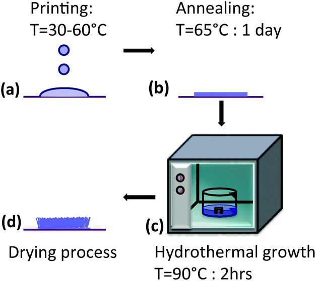 | ||
| Fig. 1 Schematic diagram of the ZnO nanowire growth procedure: (a) printing the zinc acetate dihydrate precursor, (b) annealing, (c) hydrothermal growth and (d) drying. | ||
Different configurations were used to follow the improvement in the quality of the ZnO grown nanowires. In particular, it was examined how a stage with the extra cover can affect the growth of ZnO nanowires compared to a stage with no cover at all. The next configuration tried was to set the substrate at different temperatures during printing and investigate the consequences on the morphology of the pattern of the ZnO nanowires as well as the ideal dot spacing for a continuous line formation and if it agrees with the theoretical concept.17 Further investigations were done in terms of multi-layer printing, and how it can alter the density of the nanowires.
The printer used is the Dematix Materials Printer (DMP-2831). The resulting ZnO patterns were characterized with the following tools. A SEM (LEO GEMINI 1530VP FEG-SEM) was used to image the surface morphology of the ZnO nanowires on the patterns. The Veeco Dektak 6M Stylus Surface Profilometer was used to measure the height of the patterns.
3 Results and discussion
3.1 ZnO nanowire synthesis
Once the pattern is printed, followed by annealing and then set in the nutrient solution for hydrothermal treatment, ZnO nanowires start to grow. Based on a study of Duan et al., it is claimed that zinc acetate dihydrate can free its H2O molecules by heating between 50–125 °C.18 This ensures that the dehydration step at 65 °C followed in this paper must be valid and the chemical formula should change from Zn(CH3COO)2·(H2O)2 to Zn(CH3 COO)2. Since there is no use of high boiling-point organic additives, the sample can be treated at a very low temperature. The following chemical equations represent the overall reactions taking place during the hydrothermal growth of ZnO nanowires:19| (CH2)6N4 + 6H2O ↔ 6HCHO + 4NH3 | (1) |
| NH3 + H2O ↔ NH4+ + OH− | (2) |
| 2OH− + Zn2+ ↔ Zn(OH)2(s) | (3) |
| Zn(OH)2(s) ↔ ZnO(s) + H2O | (4) |
| Zn(CH3COO)2 + 2OH− → ZnO(s) + 2CH3COO− + H2O | (5) |
Eqn (1)–(4) explain what happens in the nutrient solution. In (1), HMTA decomposes in heated aqueous solution to give ammonia and formaldehyde.20 In this way HMTA acts as a pH buffer since ammonia slowly converts into NH4+ and OH−, where the latter helps with the formation of Zn(OH)2 as shown in (3). Meanwhile, (5) shows that the anhydrous zinc acetate precursor layer converts into a ZnO seed-layer by forced hydrolysis21 that happens simultaneously with the above. Eqn (4) shows that Zn(OH)2 can convert into ZnO, and this can happen either as heterogeneous or homogeneous nucleation. The latter though requires high-supersaturated levels of Zn(OH)2, heterogeneous nucleation can happen even at low-supersaturated levels through dissolution/reprecipitation17 onto a ZnO seed-layer to form nanowires because the interfacial energy between the ZnO crystals and seed-layer is smaller than the interfacial energy between the crystals and solution.22 All these reactions except (5) are in equilibrium and can be shifted if parameters like temperature, time and concentration of nutrients change.23,24 Also, the ratio between zinc acetate dihydrate and HMTA plays a significant role too. For example, a lower concentration of HMTA to zinc acetate dihydrate would result in a reduction of the nanowire aspect ratio.25
3.2 Extra cover effect
The nanowires are supposed to grow only on the patterned areas where there is a ZnO seed layer. However, a collective amount of ZnO nanowires was also found to grow at locations adjacent to the patterned areas. The exact reasons for this are not clear but it is believed to be due to the uncontrolled flow of fluid from the natural convectional currents driven by uneven temperatures in the crystallizing dish. This dynamic motion drifts the ZnO particles that start to act as seed grains throughout the area. Although Wang et al. have accurately spotted this problem and suggested that the sample should be ideally placed floating on the surface of the solution facing downwards.26 Nevertheless, this is not enough. By adding the extra cover it restricts the immoderate convectional current, providing a steady flow that is almost static relative to the samples. This also confines the volume below the samples limiting the amount of additional unwanted suspension of particles while allowing itself to replenish over time. It is found in our case that a spacing of 1.6 mm is ideal, while a spacing of more than 1 cm does not help. Fig. 2 shows the big difference between the two configurations. It can be clearly seen that the number of unwanted ZnO nanowire clusters is significantly reduced, allowing the fabrication of clean, high quality patterns.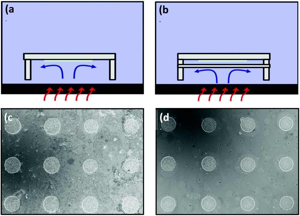 | ||
| Fig. 2 Upside-down sample during the hydrothermal process (a) without and (b) with the extra cover. Patterns of (c) and (d) correspond to (a) and (b), respectively. | ||
3.3 Platen temperature effect
The schematic diagram in Fig. 3 shows the formation of the coffee-stain and how it can be constrained in this study. It is well known that when a droplet falls on the substrate it takes a cup sphere shape. This should evaporate uniformly after some time. However, because of the presence of particles inside the drop, the contact line is pinned and because of the higher temperature at the edge, differential evaporation occurs.27,28 This leads to a thermo-capillary convection that draws the particles to points of higher evaporation rates. The final result, which is a ring-formation of aggregated particles that settle at the former drop edge, can be seen in Fig. 3d.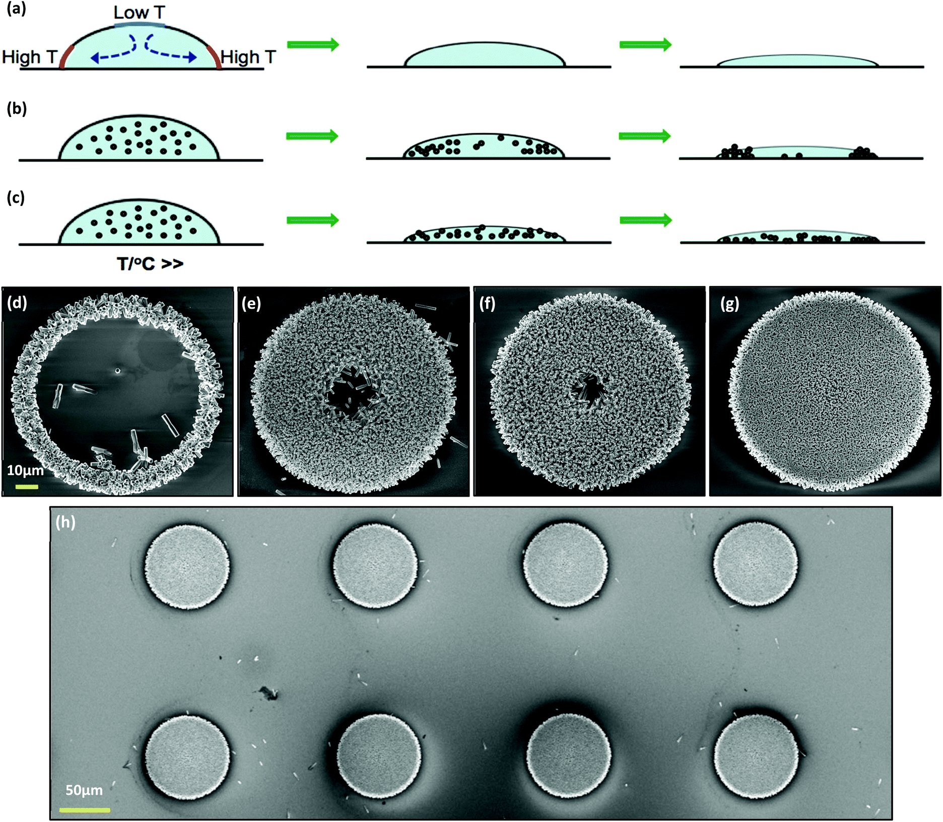 | ||
| Fig. 3 Schematic representation of the mechanism of particle distribution in drying drops. (a) A differential evaporation rate due to the temperature gradient produces a thermo-capillary flow. (b) If particles are present, they follow this flow and adhere at the contact line of the droplet. (c) At much higher temperatures, the particles disperse uniformly. SEM images of ZnO nanowire arrays grown on 1-pass printed seed particles correspond to platen temperature configurations of (d) 25 °C, (e) 40 °C, (f) 50 °C and (g) 60 °C. (h) Pattern of 2 × 4 ZnO nanowire dots at 60 °C. The diameter of dots is ∼85 μm. | ||
Different methods were tried to eliminate the coffee-stain effect. There are several reports that have printed more than one layer to fill the uncovered areas while others have developed recipes of a combination of solvents in order to establish a surface-tension gradient. This gives rise to a Marangoni flow that opposes the above flow.29,30 While this could be demonstrated to work, it can be complicated as it needs the correct combination of solvents as well as the right ratio between themselves. In fact, the extra solvent could also require higher annealing temperatures, and this can restrict the selection of substrates.
In this paper, the coffee-stain effect is successfully limited by heating the substrate above room temperature during printing. Increasing the temperature of the substrate induces a faster evaporation rate of the drop. Even if the evaporation rate is differential to some degree, at higher temperatures it becomes fast enough to overcome the thermo-capillary conventional flow from the centre to the edge. Eventually, the drop will evaporate before the particles migrate collectively to the edge allowing them to disperse uniformly. Comparing the dots in Fig. 3e–g it can be seen that there is a big difference in change from room temperature to 60 °C. The dot at 40 °C has an empty central region of nanowires while the dot at 60 °C looks very uniform along its radius and with a denser forest of nanowires. It is important to mention that we observe a change in the diameter of the nanowires themselves. In the ESI, Fig. S5–S7† show that the nanowires belonging to a 3-pass printed configuration have an average diameter of 570 nm at 40 °C, 500 nm at 50 °C and 320 nm at 60 °C.† This is most likely due to the higher density of nanowires. When several seed particles settle next to each other, they form seed-sites of slightly higher thickness than the rest of the area.31,32 These elevated sites are responsible for the heterogeneous nucleation and development of ZnO nanowires. The denser the seed particles the more nucleation sites turn up and hence the denser the nanowires. Increasing the density of nanowires restricts their lateral growth since the access of nutrients to the sidewalls of nanowires becomes more difficult.
However, there is a visible difference between the nanowires grown in the centre, compared to those grown at the edge of the patterns. What is observed is that the nanowires at the edge are usually bigger than the inner ones. For example, the nanowires grown at a substrate temperature of 40 °C have an average diameter of 1100 nm at the edge and 580 nm at the centre, whereas the ones grown at 60 °C have an average diameter of 650 nm and 450 nm respectively. This shows that by reducing the coffee-stain effect, we reduce the large variations in the morphology of nanowires across the pattern. In addition, the nanowires grown at the edge produce an urchin-like design morphology (Fig. S10, ESI†), a phenomenon quite universal in other inkjet-printed patterns too.14,15 This is possible because they follow a radial growth, which is mainly favoured by the lack of nanowires outside the patterned region. In order for nanowires to minimize their total surface energy and maintain their length, they tend to grow towards regions of higher nutrient solution. Another important factor that can contribute to this particular growth mechanism is the angular deviation of the normal axis of nucleation sites at the edge of the pattern compared to the rest of the area, especially in elevated heights.33
3.4 Continuous line formation
Digital selective patterning is one of the many advantages of inkjet printing and in order to form a desired pattern it should be able to produce continuous lines on the micron scale. To produce such lines, a series of dots must be juxtaposed with the necessary spacing. The dot spacing is the distance between two consecutive droplets that the printer ejects on the substrate. This can be configured in the printer's parameters but it does not usually give the desired outcome. Many factors such as substrate temperature, satellite droplets and ambient humidity can play an adverse role.34 In this paper, we attempt to resolve these issues by combining the characteristics of the particular precursor ink and the ideal substrate temperature. In this experiment, three configurations of dot spacing were tried: 80 μm, 60 μm and 40 μm. The temperature of the platen was set to 60 °C. By looking at Fig. 4 it is clearly seen that for the 80 μm dot spacing, the line has an irregular width where the maxima represents the dots’ diameter and minima the impinging connection between the dots. Reducing the dot spacing down to 60 μm, a nicely uniform line forms with a width of 86 μm. If the dot spacing is further reduced to 40 μm, the line width increases to 100 μm. This shows a correlation with the theory proposed by Smith et al. predicting the width of the line as being inversely proportional to the square root of dot spacing.17 However, if the dot spacing is reduced below a certain threshold value, according to Duineveld, the line width stops following the above rule and produces a series of bulges due to dynamic instabilities.35,36 Indeed, the lowest dot spacings tried in this experiment were 35 μm and 25 μm with the latter breaking the rule of a continuous straight line (Fig. S12 and S13, ESI†).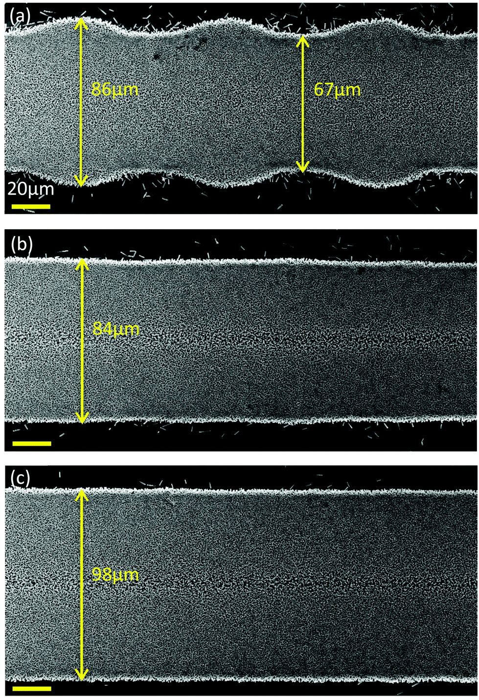 | ||
| Fig. 4 SEM images of different dot spacing configurations of (a) 80 μm, (b) 60 μm and (c) 40 μm. | ||
3.5 Multilayer effect
Printing more than one layer introduces visible changes in the morphology of the surface of patterns. First of all, the density of nanowires increases, increasing the fill factor. By printing more than one layer of precursor ink, more nanoparticles are deposited within the same area. It is believed that the number of nucleation sites increases as the printed pattern gets thicker and this leads to a higher concentration of nanowires. In addition, this impacts the orientation of nanowires too as the density of nanowires is directly related to their degree of alignment.37 The sample with the 3-pass printing reveals, as shown in Fig. S2–S5,† a denser forest of nanowires of better orientation than the sample with the 1-pass printing.† When more nanowires grow in the same area, less space is available in-between them. Therefore, in order to maintain a low surface energy they tend to grow as vertical as possible. Furthermore, the pattern of 3-pass printed seed layer (Fig. 5) appears to give shorter nanowires with smaller diameters. As discussed in section 3.3, fewer nutrients reach the nanowire sidewalls due to the limited space. This results in a slower lateral growth. As for the length of NWs, the axial growth is slower while the denser nanowires require more nutrients in the same duration of time. Finally, with the enhancement of nanowires in the vertical orientation, high density, small diameter NWs improve the dot surface pattern. Fig. 5a clearly shows that with 3 layers of printing the pattern becomes smoother with respect to one layer.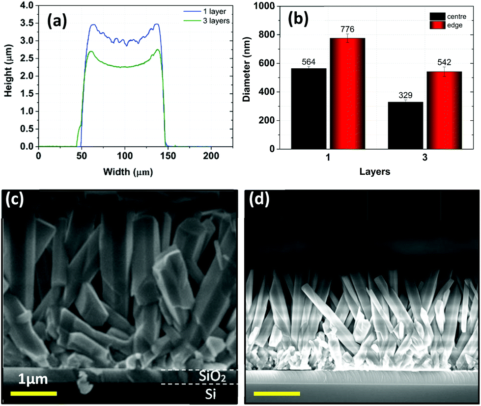 | ||
| Fig. 5 (a) Line profile of dots of ZnO nanowires grown on 1- and 3-pass printed layers. (b) Comparison of the diameters between the two configurations at both central and edge regions of dots. Cross-sectional images of dots corresponding to nanowires grown on (c) 1-pass and (c) 3-pass printed layers. These are done under optimised conditions at 60 °C. | ||
4 Conclusions
In summary, well-aligned ZnO nanowires are successfully grown by the hydrothermal method on seed layers derived from inkjet printed zinc acetate patterns. There is no requirement of vacuum conditions and strong etchants as it is intended to avoid multi-step techniques. Confining the fast-moving convectional flow of nutrient solution effectively reduces the number of unwanted nanowires grown outside the region of the patterns. The coffee-stain effect can be almost eliminated or taken advantage of when required through appropriate adjustment of the temperature of the substrate during inkjet printing. We show that the verticality of nanowires and the uniformity of the patterned surface have a direct effect on their density, which can be controlled either through temperature or the number of printed layers. Regulating the dot spacing to 2/3rd of the original printed dot size can produce continuous line formations, while giving the opportunity to modify the width of the line by decreasing the dot spacing even further. In summary, these configurations can give enough technical knowledge on producing ZnO nanowires under mild conditions thus making them compatible for applications in flexible large area electronics.Acknowledgements
This research was supported by the Engineering and Physical Sciences Research Council (EPSRC) through the Integrated Photonic and Electronic Systems (IPES) Centre for Doctoral Training and ORAMA. The author would also like to thank Dr Malik M. Qasim for his help and advice on this work.References
- K. Ellmer, J. Phys. D: Appl. Phys., 2000, 33, R17–R32 CrossRef CAS.
- E. Fortunato, P. Barquinha, L. Pereira and R. Martins, Adv. Mater., 2005, 17, 590–594 CrossRef CAS.
- A. Hatamie, A. Khan, M. Golabi, A. P. F. Turner, V. Beni, W. C. Mak, A. Sadollahkhani, H. Alnoor, B. Zargar, S. Bano, O. Nur and M. Willander, Langmuir, 2015, 31, 10913–10921 CrossRef CAS PubMed.
- J. H. Lim, C. K. Kong, K. K. Kim, I. K. Park, D. K. Hwang and S. J. Park, Adv. Mater., 2006, 18, 2720–2724 CrossRef CAS.
- Y. Qiu, D. C. Yang, B. Yin, J. X. Lei, H. Q. Zhang, Z. Zhang, H. Chen, Y. P. Li, J. M. Bian, Y. H. Liu, Y. Zhao and L. Z. Hu, RSC Adv., 2015, 5, 5941–5945 RSC.
- N. S. Ramgir, K. Subannajui, Y. Yang, R. Grimm, R. Michiels and M. Zacharias, J. Phys. Chem. C, 2010, 114, 10323–10329 CAS.
- B. D. Yao, Y. F. Chan and N. Wang, Appl. Phys. Lett., 2002, 81, 757–759 CrossRef CAS.
- W. Lee, M. Jeong and J. Myoung, Acta Mater., 2004, 52, 3949–3957 CrossRef CAS.
- A. B. Hartanto, X. Ning, Y. Nakata and T. Okada, Appl. Phys. A: Mater. Sci. Process, 2004, 78, 299–301 CrossRef CAS.
- L. Vayssieres, K. Keis, A. Hagfeldt and S. E. Lindquist, Chem. Mater., 2001, 13, 4395–4398 CrossRef CAS.
- H. W. Choi, T. Zhou and G. E. Jabbour, Nanoscale, 2015, 7, 3338–3355 RSC.
- M. Abulikemu, E. Husni, H. Haverinen, D. Cha, M. A. Malik and G. E. Jabbour, Angew. Chem., Int. Ed., 2013, 52, 1–5 CrossRef.
- M. Layani, M. Gruchko, O. Milo, I. Balberg, D. Azulay and S. Magdassi, ACS Nano, 2009, 3, 3537–3542 CrossRef CAS PubMed.
- J. Kwon, S. J. Hong, H. Lee, J. Yeo, S. S. Lee and S. H. Ko, Nanoscale Res. Lett., 2013, 8, 489 CrossRef PubMed.
- S. H. Ko, D. Lee, N. Hotz, J. Yeo, S. Hong, K. H. Nam and C. P. Grigoropoulos, Langmuir, 2012, 28, 4787–4792 CrossRef CAS PubMed.
- M. C. Akgun, Y. E. Kalay and H. E. Unalan, J. Mater. Res., 2012, 27, 1445–1451 CrossRef CAS.
- B. D. P. J. Smith, D.-Y. Shin and J. E. Stringer, J. Mater. Sci., 2006, 41, 4153–4158 CrossRef.
- Y. Duan, J. Li, X. Yang, L. Hu, Z. Wang, Y. Liu and C. Wang, J. Anal. Appl. Pyrolysis, 2008, 83, 1–6 CrossRef CAS.
- S. Xu and Z. L. Wang, Nano Res., 2011, 4, 1013–1098 CrossRef CAS.
- X. Hu, Y. Masuda, T. Ohji and K. Kato, Langmuir, 2008, 24, 7614–7617 CrossRef CAS PubMed.
- K. Govender, D. S. Boyle, P. B. Kenway and P. O. Brien, J. Mater. Chem., 2004, 14, 2575–2591 RSC.
- L. Vayssieres, K. Keis, S. Lindquist and A. Hagfeldt, J. Phys. Chem. B, 2001, 105, 3350–3352 CrossRef CAS.
- H. L. Cao, X. F. Qian, Q. Gong, W. M. Du, X. D. Ma and Z. K. Zhu, Nanotechnology, 2006, 17, 3632–3636 CrossRef CAS.
- S. Xu, N. Adiga, S. Ba, T. Dasgupta, J. Wu and Z. L. Wang, ACS Nano, 2009, 3, 1803–1812 CrossRef CAS PubMed.
- W. X. Zhang and K. Yanagisawa, Chem. Lett., 2005, 34, 1170–1171 CrossRef CAS.
- X. Wang, F. Sun, Y. Huang, Y. Duan and Z. Yin, Chem. Commun., 2015, 51, 3117–3120 RSC.
- R. D. Deegan, O. Bakajin, T. F. Dupont, G. Huber, S. R. Nagel and T. A. Witten, Lett. Nat., 1997, 389, 827–829 CrossRef CAS.
- R. Deegan, Phys. Rev. E: Stat. Phys., Plasmas, Fluids, Relat. Interdiscip. Top., 2000, 61, 475–485 CrossRef CAS.
- H. Hu and R. G. Larson, J. Phys. Chem. B, 2006, 110, 7090–7094 CrossRef CAS PubMed.
- B. J. De Gans and U. S. Schubert, Langmuir, 2004, 20, 7789–7793 CrossRef CAS PubMed.
- H. Sun, M. Luo, W. Weng, K. Cheng, P. Du, G. Shen and G. Han, Nanotechnology, 2008, 19, 395602 CrossRef PubMed.
- J. Liu, J. She, S. Deng, J. Chen and N. Xu, J. Phys. Chem. C, 2008, 112, 11685–11690 CAS.
- H.-H. Park, X. Zhang, K. W. Lee, K. H. Kim, S. H. Jung, D. S. Park, Y. S. Choi, H. Shin, H. K. Sung, K. H. Park, H. K. Kang, H. Park and C. K. Ko, CrystEngComm, 2013, 15, 3463 RSC.
- Y. N. Liang, B. K. Lok and X. Hu, Proc. Electron. Packag. Technol. Conf. EPTC, 2009, 174–179 Search PubMed.
- B. Derby, J. Eur. Ceram. Soc., 2011, 31, 2543–2550 CrossRef CAS.
- P. C. Duineveld, J. Fluid Mech., 2003, 477, 175–200 Search PubMed.
- Z. H. Ibupoto, K. Khun, M. Eriksson, M. Alsalhi, M. Atif, A. Ansari and M. Willander, Materials, 2013, 6, 3584–3597 CrossRef CAS.
Footnote |
| † Electronic supplementary information (ESI) available: Printing parameters in detail and extra figures. See DOI: 10.1039/c6nr02962k |
| This journal is © The Royal Society of Chemistry 2016 |