
 Open Access Article
 This Open Access Article is licensed under a
 Creative Commons Attribution 3.0 Unported Licence
Chirality specific and spatially uniform synthesis of single-walled carbon nanotubes from a sputtered Co–W bimetallic catalyst†
Hua
An
a,
Akihito
Kumamoto
b,
Hiroki
Takezaki
a,
Shinnosuke
Ohyama
a,
Yang
Qian
a,
Taiki
Inoue
a,
Yuichi
Ikuhara
b,
Shohei
Chiashi
a,
Rong
Xiang
*a and
Shigeo
Maruyama
*ac
aDepartment of Mechanical Engineering, The University of Tokyo, Tokyo 113-8656, Japan. E-mail: maruyama@photon.t.u-tokyo.ac.jp; xiangrong@photon.t.u-tokyo.ac.jp
bInstitute of Engineering Innovation, The University of Tokyo, Tokyo 113-8656, Japan
cEnergy NanoEngineering Laboratory, National Institute of Advanced Industrial Science and Technology (AIST), Tsukuba 305-8564, Japan
First published on 29th June 2016
Abstract
Synthesis of single-walled carbon nanotubes (SWNTs) with well-defined atomic arrangements has been widely recognized in the past few decades as the biggest challenge in the SWNT community, and has become a bottleneck for the application of SWNTs in nano-electronics. Here, we report a selective synthesis of (12, 6) SWNTs with an enrichment of 50%–70% by chemical vapor deposition (CVD) using sputtered Co–W as a catalyst. This is achieved under much milder reduction and growth conditions than those in the previous report using transition-metal molecule clusters as catalyst precursors (Nature, 2014, 510, 522). Meanwhile, in-plane transmission electron microscopy unambiguously identified an intermediate structure of Co6W6C, which is strongly associated with selective growth. However, most of the W atoms disappear after a 5 min CVD growth, which implies that anchoring W may be important in this puzzling Co–W system.
Introduction
Single-Walled carbon nanotubes (SWNTs) have been attracting much attention during the last few decades due to their unique structure and ensuing interesting electronic properties, including ultra-high carrier mobility and chirality dependent electron conductivity.1,2 Various proof-of-concept applications have been demonstrated using the unique electronic properties of this material.3–5 Though tremendous progress has been made towards the realistic applications of SWNTs, it is still widely recognized that the absence of techniques to control the structure/chirality of produced SWNTs has been a bottleneck for further development, particularly for applications in electronics and optics.Chemical vapor deposition (CVD) has been proposed to be one of the most promising methods to synthesize SWNTs with high efficiencies. However, the produced SWNTs, in almost all cases, contain both semi-conducting and metallic SWNTs with mixed chiralities. Researchers have made significant efforts to explore possible approaches towards structure selective growth from both experimental and theoretical aspects. For example, D. E. Resasco et al. reported a supported CoMo catalyzed synthesis of (6, 5) dominant SWNTs by tailoring growth conditions and supported materials.6 Y. Miyauchi et al. obtained a similar chirality enrichment in a low temperature alcohol catalytic CVD.7 J. Liu et al. claimed the synthesis of semi-conducting SWNTs by using an ethanol/methanol mixture or by water etching.8–10 J. Zhang et al. found that metallic SWNTs can be destroyed by using UV light during the growth.11 A. R. Harutyunyan et al. reported a direct synthesis of metallic SWNTs as high as 91% by modulating the ambient gas during annealing.12 Y. Chen et al. achieved selective synthesis of (9, 8) with 33.5% abundance among all species.13–15 B. Yakobson et al. demonstrated that near armchair SWNTs are kinetically favorable during growth, which results in a greater length and abundance.16 This model was later supported by B. Maruyama et al. through an in situ Raman experiment.17 More recently, they concurrently considered kinetic and thermodynamic aspects of CNT growth and explained the different enrichments under different CVD conditions.18
In spite of these advances, direct CVD synthesis of single chirality SWNTs has been believed to be challenging. One breakthrough was reported in 2014 by F. Yang et al., who claimed the selective synthesis of (12, 6) SWNTs at an enrichment of 92%.19 The key to this high selectivity is the use of the Co–W catalyst, which forms a Co7W6 alloy that structurally matches with (12, 6) SWNTs. The catalyst they used is a unique crown-type structure molecule that contains six Co atoms encapsulated with a W-based polyoxoanion shell, which favors the formation of the Co7W6 alloy at high temperature.20 If this growth selectivity is governed by catalyst structure21 regardless of the precursor molecules, preparing a catalyst by more versatile optional methods will not only verify the robustness of this Co–W combination, but may also benefit possible scalable production in the future. In this context, we present here that, with a simple sputtered Co–W catalyst, selective growth can also be achieved with a (12, 6) enrichment of 50–70%. An intermediate structure of Co6W6C is also identified by our recently proposed in-plane transmission electron microscope (TEM) technique, and is found to be strongly associated with the selective nucleation.
Results and discussion
Fig. 1a shows a representative SEM image of the as-grown SWNTs formed at a growth temperature of 750 °C. A sample grown from pure Co under the same conditions is shown as the inset for comparison. Without the presence of W, the SWNTs form into a thick mat with a high nucleation density, while in the case of Co–W, the SWNT density decreases significantly. The length of the SWNTs obtained from Co–W after a 5 min growth is usually several micrometers according to high resolution SEM and TEM observations, which shows not much difference from those obtained from pure Co. The SWNTs grown from Co–W seem to be covered with some amorphous as well as particle-like impurities. This will be further characterized and discussed later. However, since the catalyst is prepared by sputtering, in either case, SWNTs grow uniformly over the entire substrate. This spatial uniformity will be important for future device fabrications.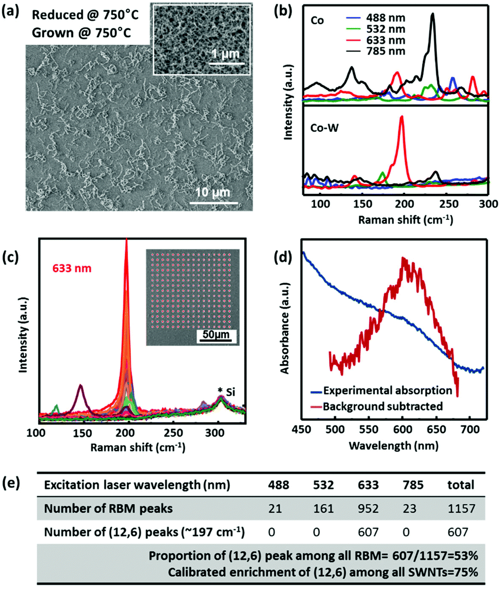 | ||
| Fig. 1 Characterization of SWNTs grown from sputtered Co-W. (a) A typical SEM image of SWNTs grown from Co-W. Inset: SWNT arrays obtained from pure Co. (b) Averaged Raman spectra in the RBM region of SWNTs grown from pure Co and Co-W with four different excitation wavelengths. (c) Raman spectra of SWNTs with multi data excited at 633 nm. (d) An optical absorption spectrum of SWNT samples after dispersion. (e) Statistical analysis on SWNTs of (12, 6) with RBM occurrence frequencies excited by four lasers: 488, 532, 633 and 785 nm. | ||
Raman spectroscopy is used to confirm the existence and the structure of SWNTs. The G-bands of both samples (grown from Co and Co–W catalyst) show typical features of SWNTs, with a clear split into G+ and G−. The D bands of both samples are not strong, and typical G/D ratios are about 15 to 20 (Fig. S1†). However, clear differences are observed between the two samples in Radial Breathing Mode (RBM) regions (Fig. 1b). In the case of pure Co, the RBM peaks from four excitation lasers demonstrate a wide distribution, while for Co–W, though SWNTs with other chiralities also exist, the peak locating at 197 cm−1 excited by a 633 nm laser becomes dominant. The index of the dominant SWNTs is assigned as (12, 6) according to the diameter and the excited transition energy in the Kataura plot (Fig. S2†). As the environment, the substrate and even the amorphous carbon coating may affect the vibration of a SWNT, the inverse relationship of the RBM frequency and the diameter of the SWNTs is determined by ωRBM = 235.9/dt + 5.5,22 which was carefully calibrated and specified for SWNTs on flat Si/SiO2 in this range. (9, 9) is excluded because of the G-band shape which shows an asymmetric G− with a Breit–Wigner–Fano (BWF) feature.23
Raman mapping was performed to obtain more quantitative results about the SWNT content. In this Raman scanning, a step of 8 μm is used. Since the spot size of the laser is smaller than 2 μm and the SWNT length is approximately 2–5 μm as obtained from SEM characterization, 8 μm spacing is reasonable to measure one SWNT only once (though in each spot there might exist more than one SWNT), and to avoid the over-counting of the same SWNT. By this approach, we measured a 1 cm × 1 cm sample by four different excitations (totally 1826 points), and obtained 1157 observable RBM peaks, within which 607 are assigned as (12, 6). From these statistics, assuming that each (12, 6) peak comes from one SWNT, the proportion of (12, 6) peaks among all detectable RBMs can be calculated to be about 53%. Considering that there are high possibilities that one peak at 197 cm−1 comes from two or more (12, 6) tubes under one laser spot, the real enrichment of (12, 6) tubes can be higher. In the original report, F. Yang et al.19 observed approx. seven SWNTs under one laser spot and concluded a selectivity of over 90%. Assuming that there are x SWNTs on average under one laser spot, the enrichment in this sample can be calibrated to be 67%, 75%, 82%, and 89% if x equals to 2, 3, 4, and 7, respectively. In our case, the SWNTs are sparser and there are usually 3 to 4 SWNTs on average under one laser spot, so (12, 6) enrichment after this calibration is over 70% with conservative estimation. We claim that this number does not always reflect the exact percentage in SWNTs, because there could be other SWNTs that are not resonant at all these four excitation wavelengths (due to the well-known resonance effect), and/or some SWNTs could be too short to be identified from the background. However, it seems to be clear that the produced SWNT sample is highly (12, 6) enriched according to this Raman analysis, and we conclude here that the enrichment is 50–70% from the current Raman analysis.
Optical absorption usually gives more reliable evaluations of the entire sample. Fig. 1d shows a dominant absorption peak at ∼610 nm, which is consistent with the M11 transition of (12, 6) SWNTs. However, due to the low SWNT yield, the peak is not satisfactorily strong, though over 30 samples were used to prepare one solution. Also, the broad peak suggests the possible coexistence of impurities and other SWNTs. Possibly because of these two reasons; we cannot observe a peak splitting that was clearly shown for spectroscopically pure semimetal SWNTs.24,25 Compared with the original report of over 90%,19 this relatively low selectivity could be related to the lower growth temperature and/or to a different catalyst preparation method. Except for this, it is convincing to us that the incorporation of W into a Co catalyst leads to a clear shift and narrowing down of the chirality distribution.
The reduction temperature of the catalyst is found crucial for SWNT yield as well as for the selectivity of (12, 6) SWNTs. Fig. 2 shows SEM images and the corresponding average Raman spectra of SWNTs grown from the catalyst reduced at different temperatures. In all three cases, the growth temperature was set the same (750 °C) to compare the possible structure change of the catalyst during reduction. When the reduction temperature is low (600 °C), the SWNT yield is much higher than that of the other two samples. The Raman spectrum suggests that this low temperature reduced sample is very similar to those grown from pure Co (Fig. S3†). The relative intensity of the 197 cm−1 peak (to other peaks) is remarkably decreased. For the samples grown from the higher temperature (750 °C) reduced catalyst, however, the (12, 6) peak significantly dominates the RBM peaks (SWNT yield decreases to 5% roughly estimated from Raman). When the reduction temperature goes up to 850 °C, the selectivity slightly improves but the yield becomes much lower. The changes in relative intensities at the 197 cm−1 peak with respect to the total sum intensity are shown in Fig. S4,† revealing a developing selectivity with the increasing reduction temperature. This trend suggests that despite the reduction at this relatively low temperature, the introduction of W is still effective for the selectivity, which indicates that the catalyst structure may have already changed. Compared to the original report by F. Yang et al.,19 where they claimed that 1030 °C is necessary, nearly 300 °C lower reduction/growth temperature is puzzling. If not explainable by a further downshift of the bulk phase diagram and therefore the easier formation of the alloy at lower temperatures, there might be some other un-identified factors that are playing a critical role.
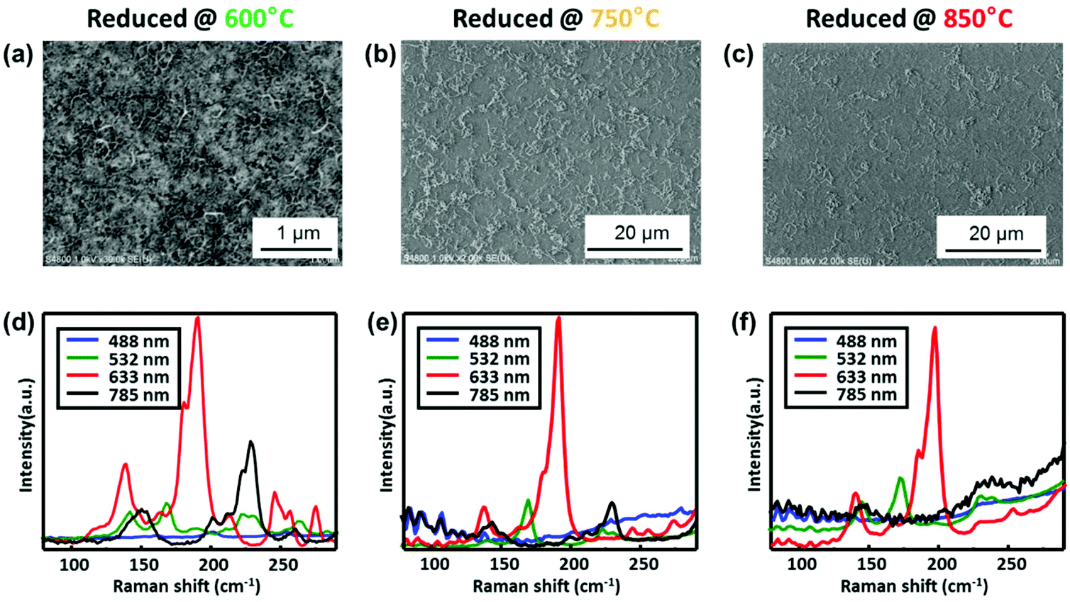 | ||
| Fig. 2 SEM images and average Raman spectra of SWNTs grown at different reduction temperatures: (a, d) 600 °C, (b, e) 750 °C and (c, f) 850 °C. | ||
In order to tackle this puzzle, we further performed an in-plane TEM study on these sputtered Co–W catalysts. In these experiments, the Co–W catalysts are directly prepared onto a SiO2 TEM grid. The advantage of this technique is that this TEM grid can be used for high temperature reactions.26 Though atomic resolution is not always easy due to the thick SiO2 background, the most original and realistic catalyst morphology and structure are retained. Furthermore, the in-plane view also provides a chance to access the statistical information of one sample, which is hardly obtainable in conventional TEM observations.
Fig. 3 shows representative TEM images of samples grown at 750 °C but were reduced at different temperatures (similar to samples in Fig. 2). In Fig. 3a and b, clear differences in the catalyst morphology are observed between the two samples. At a low reduction temperature (600 °C), W and/or C atoms migrate and form a wormlike/island structure, which may be a transition morphology from an as-deposited continuous film (not shown) to nano-sized particles. The 750 °C reduced catalyst (Fig. 3b), however, shows a more complex and polycrystal-like contrast. Though the melting temperature of W is 3422 °C in bulk, it is apparent that W starts to aggregate and form irregular particles at a temperature as low as 750 °C. Particularly, the regions near larger W particles seem to have been “swallowed” by the center. Therefore, possibly from this stage, W begins to form an alloy/composite with Co, and those particles with a complex contrast contain both Co and W (structure to be determined later). The 850 °C reduced catalysts in Fig. 3c show a particle-like morphology similar to the 750 °C reduced sample, except that the particles are more spherical and the number density is slightly smaller. The simplified illustrations of these changes are shown as the insets of Fig. 3a–c. The in-plane images of these samples after SWNT growth are shown in Fig. 3d–f. The most noticeable difference is the SWNT yield, which agrees well with the SEM and Raman observation (Fig. 2). At the same time, all three samples contain particles with a diameter of 5–30 nm, which are possibly those impurities in SEM observations discussed previously. Besides these three representative samples, we also grew SWNTs from 650 °C, 700 °C and 800 °C reduced catalysts, which show intermediate morphologies (Fig. S5†). Three reduction temperatures are shown here to demonstrate a clearer trend from islands to spherical particles. In all these observations, identifying the contrast of SWNTs is very difficult due to the strong background of SiO2. Few layer graphite sheets are sometimes observed on large particles (possibly excess of W as to be discussed later), but no few- or multi-walled carbon nanotubes exist.
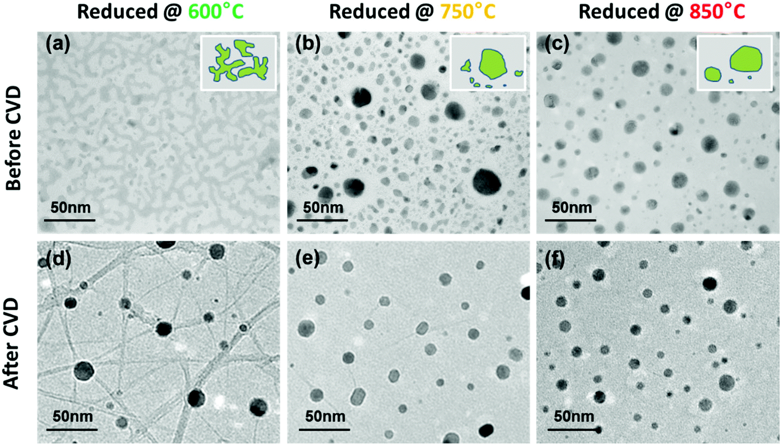 | ||
| Fig. 3 TEM micrographs of different temperature reduced (600 °C, 750 °C and 850 °C, respectively) Co-W catalysts. (a), (b), and (c) Before CVD and (d), (e), and (f) after a 5 min growth at 750 °C. | ||
One uniqueness of in-plane TEM is its capability of providing comprehensive structural information in a large area. We compared the selected area electron diffraction (SAED) patterns of the samples before and after growth, as shown in Fig. 4. In this experiment, each diffraction pattern was taken with the selected area aperture diameter of several micrometers, and therefore contains the average information of more than 10![[thin space (1/6-em)]](https://www.rsc.org/images/entities/char_2009.gif) 000 particles. Lower-temperature reduced samples show a clear and dominant phase of the BCC structure of metallic W (JCPDS-International Centre for Diffraction Data 2004, card no. PDF#04-0806). Co is not visible possibly due to the lower relative amount, alloying with W and/or oxidized after exposure to air. However, since the obtained SWNTs are very similar to those from pure Co, probably the interaction between Co and W at this lower temperature is less significant and most SWNTs are grown from pure Co. For the high temperature reduced catalysts, additional diffraction rings appear at around 110 of metallic W (Fig. 4a), suggesting the formation of a new crystal phase. These diffraction rings match perfectly with Co6W6C (card no. PDF#23-0939). Though the as-reduced catalyst is not supposed to have carbon, this structure is consistently identified in all our experiments where selective growth is achieved. This un-intentionally incorporated carbon (possibly from carbon contamination and/or residue in CVD apparatus) may contribute to the formation of Co6W6C. This influence of un-intentionally introduced species is not unique and is also reported previously in an Fe-based system.27 Since no additional Co related diffraction patterns are observed, it is very likely that this structure is responsible for the nucleation of SWNTs. At this stage, we are not able to rule out the possibility of coexistence of some small amounts of metallic Co particles. However, according to the control experiment described previously, pure Co tends to grow SWNTs with a wide chirality distribution and thus is unlikely dominant in this case (Fig. S6†). Except this ternary Co6W6C, no other Co–W alloy phases, e.g. Co7W6, are identified in all our experiments.
000 particles. Lower-temperature reduced samples show a clear and dominant phase of the BCC structure of metallic W (JCPDS-International Centre for Diffraction Data 2004, card no. PDF#04-0806). Co is not visible possibly due to the lower relative amount, alloying with W and/or oxidized after exposure to air. However, since the obtained SWNTs are very similar to those from pure Co, probably the interaction between Co and W at this lower temperature is less significant and most SWNTs are grown from pure Co. For the high temperature reduced catalysts, additional diffraction rings appear at around 110 of metallic W (Fig. 4a), suggesting the formation of a new crystal phase. These diffraction rings match perfectly with Co6W6C (card no. PDF#23-0939). Though the as-reduced catalyst is not supposed to have carbon, this structure is consistently identified in all our experiments where selective growth is achieved. This un-intentionally incorporated carbon (possibly from carbon contamination and/or residue in CVD apparatus) may contribute to the formation of Co6W6C. This influence of un-intentionally introduced species is not unique and is also reported previously in an Fe-based system.27 Since no additional Co related diffraction patterns are observed, it is very likely that this structure is responsible for the nucleation of SWNTs. At this stage, we are not able to rule out the possibility of coexistence of some small amounts of metallic Co particles. However, according to the control experiment described previously, pure Co tends to grow SWNTs with a wide chirality distribution and thus is unlikely dominant in this case (Fig. S6†). Except this ternary Co6W6C, no other Co–W alloy phases, e.g. Co7W6, are identified in all our experiments.
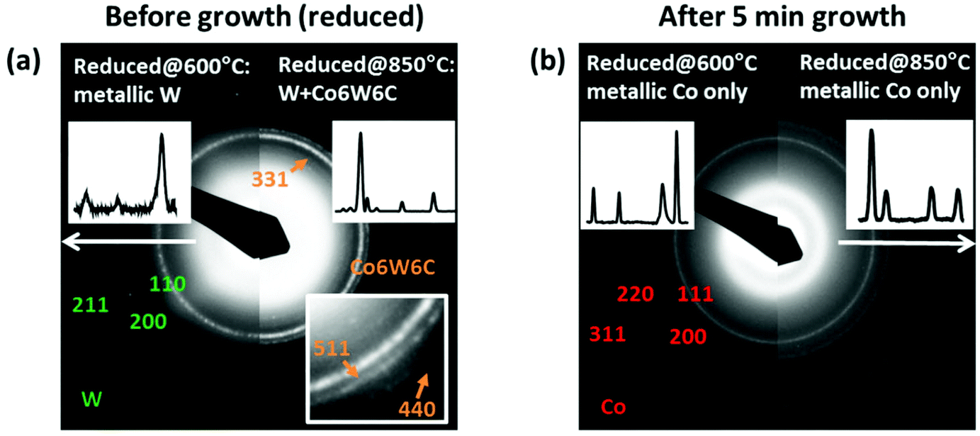 | ||
| Fig. 4 Electron diffraction patterns of catalysts reduced at 600 °C and 850 °C. (a) Before and (b) after growth with the assigned materials and structure. The insets are the relative intensity of electron diffraction rings. | ||
Another interesting phenomenon that we found here is that after growth, in both low and high temperature reduced samples, W related phases disappear almost completely. Neither noticeable metallic W nor any other W related phases remain after a 5 min growth. Only the existence of pure metallic Co was confirmed by the SAED patterns in Fig. 4b. The loss of W species is likely due to a reaction with ethanol during the SWNT growth. Ethanol molecules partially decompose at the CVD temperature with water and ethylene as the main products.28 At the same time, metallic W is reported to be easily oxidized in a water vapor environment to form volatile WO2(OH)2, which can easily disappear at high temperatures through the gas phase.29 This dynamic change of the catalyst structure makes it more challenging to identify the active nucleation sites for growth, which suggests that growth time is another important parameter for more precise control over selective growth. Further studies may be focused on CVD time dependent (12, 6) enrichment. Meanwhile, the yield in the present study is extremely low and we are not yet able to increase carbon yield without compensation of selectivity. Also, it is still unclear whether high selectivity and low yield are always strongly coupled (e.g. an earlier work showed no chirality selectivity for Co–W at a higher carbon yield30). Besides growth, more sophisticated characterization may be needed for more precise quantification (e.g. a laser close to 633 nm may excite more SWNT “impurities” that have diameter close to 1.2 nm but are not resonant in current measurement). Nevertheless, we believe that the capability of the Co–W bimetallic catalyst in selective growth is well reproduced and the critical role of W in changing the catalyst structure has been clearly demonstrated. Importantly in this work, the catalyst is prepared by simple sputtering, which is preferable for future larger scale, more uniform synthesis of SWNTs, and hopefully potential applications using chirality specific SWNT samples. This study also brings out more open questions for this complicated system, which definitely needs more effort from the whole community.
Conclusions
In summary, we demonstrated a Co–W catalyst prepared by simple sputtering, which is capable of producing (12, 6) SWNTs with a selectivity of 50–70% under much milder growth conditions. Reduction of the catalyst is crucial for selective growth, which only occurs when the reduction temperature is above 750 °C. In-plane TEM revealed clear morphological differences between low-temperature and high-temperature reduced catalysts. An intermediate structure of Co6W6C is unambiguously identified and associated with selective growth of (12, 6) SWNTs. However, the W related structure is also found to be surprisingly unstable in a growth atmosphere after only a few minutes of growth, suggesting that more effort is needed for more precise control of this complex Co–W catalyst.Experimental methods
Catalyst preparation
The Co–W catalyst is prepared by magnetron sputtering (Ulvac-Riko). The p-doped Si substrate with a 300-nm layer of SiO2 is attached to the substrate holder and metallic W (nominal thickness 0.7 nm) and metallic Co (nominal thickness 0.3 nm) are deposited in sequence followed by a 5 min annealing at 400 °C in air. The prepared substrate is used for CVD growth.SWNT growth
SWNTs are synthesized by alcohol catalytic chemical vapor deposition (ACCVD).31 Briefly, the prepared substrate is placed in a 1 inch quartz tube. A 300 sccm Ar/H2 (3%) mixture gas is purged through the tube during the heating process at a pressure of 40 kPa. Upon reaching the reduction temperature, the sample is kept for another 5 min before heating or cooling to 750 °C in an Ar atmosphere (SWNTs are grown at 750 °C in all cases). After that, ethanol is introduced at a flow rate of 150–450 sccm for a 5 min growth at the total pressure of 1.3 kPa. Finally, the tube is cooled down to room temperature with 300 sccm Ar.SWNT characterization
As-grown SWNTs are characterized by using a scanning electron microscope (SEM, Hitachi S-4800) at an accelerating voltage of 1 kV. Raman spectra are obtained by using Renishaw inVia, with excitation wavelengths of 488, 532, 633, and 785 nm. Optical absorptions are obtained on the dispersed samples by using a UV-vis-NIR optical spectrometer (Shimadzu UV-3150). Since the SWNT yield on the surface is not high enough, 30 pieces of 1 cm × 1 cm samples are sonicated in D2O solution with 1.25 w/v% SDS to obtain sufficient optical density.In-plane TEM
For in-plane TEM characterization, the Co–W catalyst is directly sputtered onto a Si/SiO2 TEM grid with a SiO2 (20 nm) fabricated by standard photolithography and etching. The prepared SiO2 grid is then used for the growth of SWNTs together with the standard Si/SiO2 wafer substrate. TEM images are obtained by using JEM-2000EX-II (JEOL Co. Ltd) and JEM-2010F (JEOL Co., Ltd) operated at 200 keV, and selected area electron diffraction (SAED) patterns are obtained by using JEM-2010F with a camera length of 60 cm.Acknowledgements
We thank T. Ito and H. Tsunakawa for TEM assistance. H. A. thanks the China Scholarship Council for financial support. Part of this work is financially supported by JSPS KAKENHI Grant-in-Aid for Scientific Research (25630063, 15H05760, 26420135), Grant-in-Aid for Young Scientists (15K17984) and JST-EC DG RTD Coordinated Research Project ‘IRENA’ under the Strategic International Collaborative Research Program (JST-SICORP), and by the “Nanotechnology Platform” (project No. 12024046) of the Ministry of Education, Culture, Sports, Science and Technology (MEXT), Japan.Notes and references
- R. Saito, G. Dresselhaus and M. S. Dresselhaus, Physical properties of Carbon Nanotubes, Imperial Collage Press, 2007 Search PubMed.
- J. Ado, G. Dresselhaus and M. S. Dresselhaus, Carbon Nanotubes - Advanced Topics in the Synthesis, Structure, Properties and Applications, Springer, 2008 Search PubMed.
- S. J. Kang, C. Kocabas, T. Ozel, M. Shim, N. Pimparkar, M. A. Alam, S. V. Rotkin and J. A. Rogers, Nat. Nanotechnol., 2007, 2, 230–236 CrossRef CAS PubMed.
- M. M. Shulaker, G. Hills, N. Patil, H. Wei, H. Y. Chen, H. S. PhilipWong and S. Mitra, Nature, 2013, 501, 526–530 CrossRef CAS PubMed.
- A. Javey, J. Guo, Q. Wang, M. Lundstrom and H. J. Dai, Nature, 2003, 424, 654–657 CrossRef CAS PubMed.
- G. Lolli, L. A. Zhang, L. Balzano, N. Sakulchaicharoen, Y. Q. Tan and D. E. Resasco, J. Phys. Chem. B, 2006, 110, 2108–2115 CrossRef CAS PubMed.
- Y. H. Miyauchi, S. H. Chiashi, Y. Murakami, Y. Hayashida and S. Maruyama, Chem. Phys. Lett., 2004, 387, 198–203 CrossRef CAS.
- L. Ding, A. Tselev, J. Y. Wang, D. N. Yuan, H. B. Chu, T. P. McNicholas, Y. Li and J. Liu, Nano Lett., 2009, 9, 800–805 CrossRef CAS PubMed.
- W. W. Zhou, S. T. Zhan, L. Ding and J. Liu, J. Am. Chem. Soc., 2012, 134, 14019–14026 CrossRef CAS PubMed.
- J. H. Li, C. T. Ke, K. H. Liu, P. Li, S. H. Liang, G. Finkelstein, F. Wang and J. Liu, ACS Nano, 2014, 8, 8564–8572 CrossRef CAS PubMed.
- G. Hong, B. Zhang, B. H. Peng, J. Zhang, W. M. Choi, J. Y. Choi, J. M. Kim and Z. F. Liu, J. Am. Chem. Soc., 2009, 131, 14642–14643 CrossRef CAS PubMed.
- A. R. Harutyunyan, G. G. Chen, T. M. Paronyan, E. M. Pigos, O. A. Kuznetsov, K. Hewaparakrama, S. M. Kim, D. Zakharov, E. A. Stach and G. U. Sumanasekera, Science, 2009, 326, 116–120 CrossRef CAS PubMed.
- H. Wang, B. Wang, X. Y. Quek, L. Wei, J. W. Zhao, L. J. Li, M. B. Chan-Park, Y. H. Yang and Y. A. Chen, J. Am. Chem. Soc., 2010, 132, 16747–16749 CrossRef CAS PubMed.
- H. Wang, L. Wei, F. Ren, Q. Wang, L. D. Pfefferle, G. L. Haller and Y. Chen, ACS Nano, 2013, 7, 614–626 CrossRef CAS PubMed.
- L. Wei, B. Liu, X. Wang, H. Gui, Y. Yuan, S. Zhai, A. K. Ng, C. Zhou and Y. Chen, Adv. Electron. Mater., 2015, 1, 1500151 CrossRef.
- F. Ding, A. R. Harutyunyan and B. I. Yakobson, Proc. Natl. Acad. Sci. U. S. A., 2009, 106, 2506–2509 CrossRef CAS PubMed.
- R. Rao, D. Liptak, T. Cherukuri, B. I. Yakobson and B. Maruyama, Nat. Mater., 2012, 11, 213–216 CrossRef CAS PubMed.
- V. I. Artyukhov, E. S. Penev and B. I. Yakobson, Nat. Commun., 2014, 5, 4892 CrossRef CAS PubMed.
- F. Yang, X. Wang, D. Q. Zhang, J. Yang, D. Luo, Z. W. Xu, J. K. Wei, J. Q. Wang, Z. Xu, F. Peng, X. M. Li, R. M. Li, Y. L. Li, M. H. Li, X. D. Bai, F. Ding and Y. Li, Nature, 2014, 510, 522–524 CrossRef CAS PubMed.
- S. Yao, Z. Zhang, Y. Li and E. Wang, Dalton Trans., 2010, 39, 3884–3889 RSC.
- F. Yang, X. Wang, D. Q. Zhang, K. Qi, J. Yang, Z. Xu, M. H. Li, X. L. Zhao, X. D. Bai and Y. Li, J. Am. Chem. Soc., 2015, 137, 8688–8691 CrossRef CAS PubMed.
- D. Zhang, J. Yang, F. Yang, R. Li, M. Li, D. Ji and Y. Li, Nanoscale, 2015, 7, 10719–10727 RSC.
- E. H. Hároz, J. G. Duque, W. D. Rice, C. G. Densmore, J. Kono and S. K. Doorn, Phys. Rev. B, 2011, 84, 121403 CrossRef.
- X. M. Tu, A. R. H. Walker, C. Y. Khripin and M. Zheng, J. Am. Chem. Soc., 2011, 133, 12998–13001 CrossRef CAS PubMed.
- E. H. Hároz, J. G. Duque, X. M. Tu, M. Zheng, A. R. H. Walker, R. H. Hauge, S. K. Doorn and J. Kono, Nanoscale, 2013, 5, 1411–1439 RSC.
- K. Cui, A. Kumamoto, R. Xiang, H. An, B. Wang, T. Inoue, S. Chiashi, Y. Ikuhara and S. Maruyama, Nanoscale, 2016, 8, 1608–1617 RSC.
- B. C. Bayer, C. Baehtz, P. R. Kidambi, R. S. Weatherup, C. Mangler, J. Kotakoski, C. J. L. Goddard, S. Caneva, A. Cabrero-Vilatela, J. C. Meyer and S. Hofmann, Appl. Phys. Lett., 2014, 105, 143111 CrossRef.
- R. Xiang, B. Hou, E. Einarsson, P. Zhao, S. Harish, K. Morimoto, Y. Miyauchi, S. Chiashi, Z. K. Tang and S. Maruyama, ACS Nano, 2013, 7, 3095–3103 CrossRef CAS PubMed.
- B. Zhou, S. Han, R. Raja and G. A. Somorjai, Nanotechnology in catalysis 3, Springer Science & Business Media, 2007 Search PubMed.
- J. E. Herrera and D. E. Resasco, J. Phys. Chem. B, 2003, 107, 3738–3746 CrossRef CAS.
- S. Maruyama, R. Kojima, Y. Miyauchi, S. Chiashi and M. Kohno, Chem. Phys. Lett., 2002, 360, 229–234 CrossRef CAS.
Footnote |
| † Electronic supplementary information (ESI) available: Raman spectroscopy (G-band) of SWNTs grown from Co and Co–W catalyst; Kataura plot for chirality assignment; Raman spectra (RBM region) of SWNTs grown from low temperature reduced monometallic Co; relative intensities of the 197 cm−1 peak with respect to the total sum intensity; TEM image of Co–W catalyst reduced at six different temperatures (600, 650, 700, 750, 800, and 850 °C); TEM images of SWNTs grown from Co monometallic catalyst. See DOI: 10.1039/c6nr02749k |
| This journal is © The Royal Society of Chemistry 2016 |