
 Open Access Article
 This Open Access Article is licensed under a Creative Commons Attribution-Non Commercial 3.0 Unported Licence
Growth and characterization of epitaxially stabilized ceria(001) nanostructures on Ru(0001)
Jan Ingo
Flege
*ab,
Jan
Höcker
a,
Björn
Kaemena
a,
T. Onur
Menteş
c,
Alessandro
Sala
c,
Andrea
Locatelli
c,
Subhashis
Gangopadhyay
d,
Jerzy T.
Sadowski
 e,
Sanjaya D.
Senanayake
f and
Jens
Falta
ab
e,
Sanjaya D.
Senanayake
f and
Jens
Falta
ab
aInstitute of Solid State Physics, University of Bremen, Otto-Hahn-Allee 1, 28359 Bremen, Germany. E-mail: flege@ifp.uni-bremen.de; Fax: +49 421 218 62251; Tel: +49 421 218 62243
bMAPEX Center for Materials and Processes, University of Bremen, 28359 Bremen, Germany
cElettra-Sincrotrone Trieste S.C.p.A., S.S. 14 - km 163, 5 in AREA Science Park, 34149 Trieste, Italy
dDepartment of Physics, BITS Pilani, Pilani 333 031, Rajasthan, India
eCenter for Functional Nanomaterials, Brookhaven National Laboratory, Upton, NY 11973, USA
fChemistry Department, Brookhaven National Laboratory, Upton, New York 11973, USA
First published on 3rd May 2016
Abstract
We have studied (001) surface terminated cerium oxide nanoparticles grown on a ruthenium substrate using physical vapor deposition. Their morphology, shape, crystal structure, and chemical state are determined by low-energy electron microscopy and micro-diffraction, scanning probe microscopy, and synchrotron-based X-ray absorption spectroscopy. Square islands are identified as CeO2 nanocrystals exhibiting a (001) oriented top facet of varying size; they have a height of about 7 to 10 nm and a side length between about 50 and 500 nm, and are terminated with a p(2 × 2) surface reconstruction. Micro-illumination electron diffraction reveals the existence of a coincidence lattice at the interface to the ruthenium substrate. The orientation of the side facets of the rod-like particles is identified as (111); the square particles are most likely of cuboidal shape, exhibiting (100) oriented side facets. The square and needle-like islands are predominantly found at step bunches and may be grown exclusively at temperatures exceeding 1000 °C.
1. Introduction
When combining different materials with distinct physical, chemical, and electronic characteristics in the nanoscale regime, their shared interface has a decisive influence on their joint properties. For transition metals and metal oxides, which are the typical components of heterogeneous catalysts, this metal–oxide interface is generally assumed to enhance the catalytic activity of the multicomponent system beyond the individual contributions of the different components.1,2 This mutual modification may occur in several forms, ranging from purely structural aspects to electronic effects (charge transfer) as well as chemical processes (intermixing), which may be used to tailor the catalyst's functionality. In case of effects related to the crystallographic structure of ordered materials, the existence of epitaxial relations at the interface may have pronounced consequences for the resulting morphology. Accordingly, optimization by rational design requires the understanding of the underlying physical and chemical processes that ultimately determine the characteristics of the multicomponent architecture. For this reason, the study of the structural, chemical, and electronic materials properties demands the application of a variety of experimental techniques to make this kind of bottom-up approach interesting for large-scale manufacturing and processing. Here, we focus on the interface of ceria, a multivalent rare-earth oxide with many applications in catalysis as well as energy harvesting, storage and conversion,3 and ruthenium, a prototypical transition metal.Of the low-index surfaces (001), (110), and (111) of cerium dioxide, the (001) has the highest energy and is the least stable with a bulk-truncated polar termination and relatively open surface;4 yet the (001) surface is very commonly found exposed in nanostructures synthesized from wet chemical methods such as rods, cubes, and spheres.5 The ability to prepare nanostructured oxides of cerium is considered an important step towards the control of reactions by tuning surface and bulk morphology of catalyst supports. The surface chemistry of the (001) surface is often compared to that of the (111) surface, with interesting variations in the structure sensitivity towards the formation of intermediates, including surface bonding and also selectivity to desorption of products.6 However, on many transition metal surfaces, the deposition of cerium oxide by evaporation of Ce metal in an oxygen atmosphere at elevated substrate temperatures typically results in the formation of (111)-oriented CeO2 islands,7–17 at conditions that are therefore thought to be representing growth near thermodynamic equilibrium. Yet, on Cu(111) also CeO2(001) islands were identified coexisting with the CeO2(111) majority phase,18–20 opening up the exciting possibility to investigate the chemistry6,21 of more open ceria surfaces with sophisticated surface science probes.22 Previously, these open surfaces had only been realized as rather thick films in the few hundred nanometer range,23–26 prohibiting a direct comparison under identical conditions.
On ruthenium(0001), and at temperatures of about 700 °C or higher, single-crystalline ceria(111) islands nucleate at step edges, and they subsequently adopt a triangular shape if not impeded by step bunches.27 Depending on substrate temperature and terrace width, these islands exhibit a typical height of 2–3 nm and may easily grow to micrometer dimensions, with an Arrhenius-like dependence of the nucleation density on substrate temperature.17 Very recently, on ruthenium both square- and rectangular-shaped CeO2(001) islands have also been observed after annealing in oxygen at temperatures up to 830 °C, and the driving force for this process has tentatively been tied to thermal reduction of the ceria that would alleviate the polarity problem.28 Here, using in situ low-energy electron microscopy (LEEM) we will show that these nanocrystals are thermodynamically stable during and after growth in a wide range of temperatures. Strikingly, at temperatures higher than 1000 °C, i.e. slightly lower than the ceria decomposition temperature at near-ultrahigh-vacuum (UHV) pressures, we find exclusively rectangular islands while the growth of (111) oriented particles is largely suppressed. Employing a suite of experimental tools comprising both in situ and ex situ microscopy, micro-diffraction, and synchrotron-based microspectroscopic techniques, we identify the structure and oxidation state of the particles and show that there is a preferred azimuthal registry with respect to the substrate main symmetry directions, enhancing the stability of the (001) oriented oxide particles that outweighs the thermodynamic preference of the ceria(111) phase.
2. Experimental methods
The Ru(0001) single crystals (Mateck) were initially cleaned ex situ and subsequently in situ using established procedures, which involve repeated oxidation by exposure to O2 and high-temperature annealing as described elsewhere.29,30 Cerium oxide was deposited in situ by evaporating metallic Ce onto the clean Ru(0001) substrate using a home-built electron beam evaporator in the main chamber of the microscope while backfilling with molecular oxygen at a partial pressure of 5 × 10⁻⁷ Torr. During growth, the sample temperature was held fixed at different temperatures ranging between 800 and 1050 °C.The LEEM experiments were performed in three separate commercial Elmitec LEEM III systems installed at the University of Bremen, Germany, at the Nanospectroscopy beamline31 at the Elettra synchrotron light source, Trieste, Italy, and at beamline U5UA of the National Synchrotron Light Source (NSLS) at Brookhaven National Laboratory (BNL), Upton, NY (USA).32 The latter two setups are additionally equipped with energy filters enabling operation as spectroscopic photoemission and low-energy electron microscopes (SPE-LEEM). This allows for in situ microscopy either by employing low-energy electrons from the internal electron gun or by using photoelectrons emitted from the sample, which are excited by the incident synchrotron radiation in an energy range of about 20–200 eV (BNL) or 20–1000 eV (Elettra). The latter enabled the recording of spatially resolved Ce M-edge absorption spectra in photoemission electron microscopy (PEEM) mode by tuning the photon energy through the range of about 860 to 910 eV and monitoring the intensity of the secondary electrons produced by the cascade of inelastic processes following the primary excitation of the photoelectron.33 The PEEM measurements were performed with a mild O2 background pressure of 2 × 10⁻⁸ mbar to avoid beam-induced reduction of the ceria nanoparticles.
Scanning tunneling microscopy was conducted in a separate UHV chamber at the University of Bremen, Germany, offering routine complementary characterization by LEED and X-ray photoelectron spectroscopy (XPS) using a conventional Mg/Al dual X-ray anode (Omicron). Further topographic information was obtained from ex situ atomic force microscopy (AFM) using a commercial Veeco V Multimode instrument at the Center for Functional Nanomaterials (CFN), BNL. Part of the data were analyzed using the open source software package GXSM developed by P. Zahl.34
3. Results and discussion
First, we will discuss the growth characteristics of cerium oxide on ruthenium(0001) at high temperatures (≥800 °C) with a particular focus on sample morphology and particle shape, covering the range from the nanometer to the micrometer scale using AFM and LEEM. In the following section, we will ascertain the chemical state of the different micro- and nanoparticles by spatially resolved X-ray absorption spectroscopy (μXAS), facilitating a probing depth of 10 nm or more due to the strongly increased escape depth of slow secondary electrons, which exhibit kinetic energies of just a few electron volts, allowing assessing the chemical state of single, whole particles. Finally, we characterize the atomic structure of the rectangular nanocrystals by reciprocal-space (μLEED) and real-space (STM) methods and establish the preferred epitaxial relation of the ceria(001) particles to the underlying substrate and give qualitative reasons for the enhanced stability observed.3.1. Growth mode and particle shape
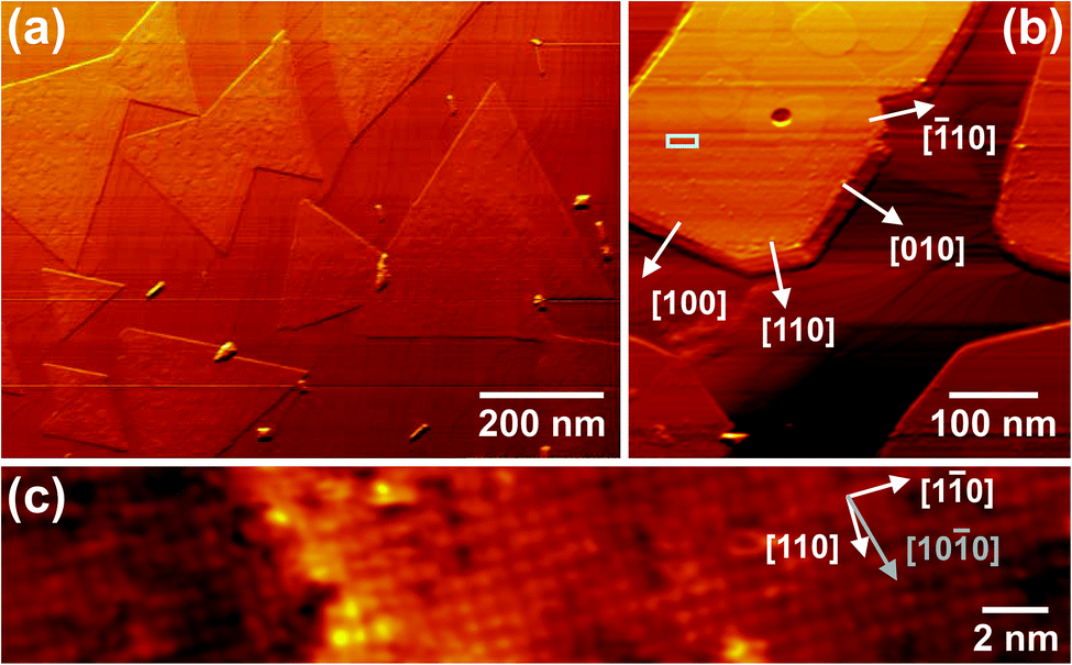
The growth of cerium oxide on the Ru(0001) surface at 800 °C and a partial O2 pressure of 5 × 10⁻⁷ Torr proceeds in the Volmer–Weber mode as displayed in Fig. 1a. Interestingly, apart from the well-known triangular-shaped, micron-sized islands (labeled “A”) that have previously been identified as CeO2(111),17 square-shaped (“B”) and rod-like objects (“C”) are observed, with relative surface coverages of 87%, 6%, and 7%, respectively, as determined from Fig. 1a. These morphological features B and C are exclusively found at steps or, especially pronounced, at massive step bunches (Fig. 1b). Different from the (111) majority phase, which appears in bright contrast at certain energies, these objects almost always appear in dark contrast compared to the oxygen-covered Ru surface and the ceria(111) phase; moreover, they display a distinct modulation of the electron reflectivity in the whole range of kinetic energies investigated (0–50 eV). This systematic difference in local energy-dependent electron reflectivity in contrast to the ceria(111) particles clearly points to a different atomic structure.35 Moreover, the rod-like objects have preferentially grown along the high symmetry directions of the hexagonal substrate, indicating a specific epitaxial relation between them. This effect is clearly visible in the magnified view of the flat-top mesa-like structure of the ruthenium substrate in Fig. 1b, where the rods are found to be oriented either in parallel or to comprise angles of 60 or 120°.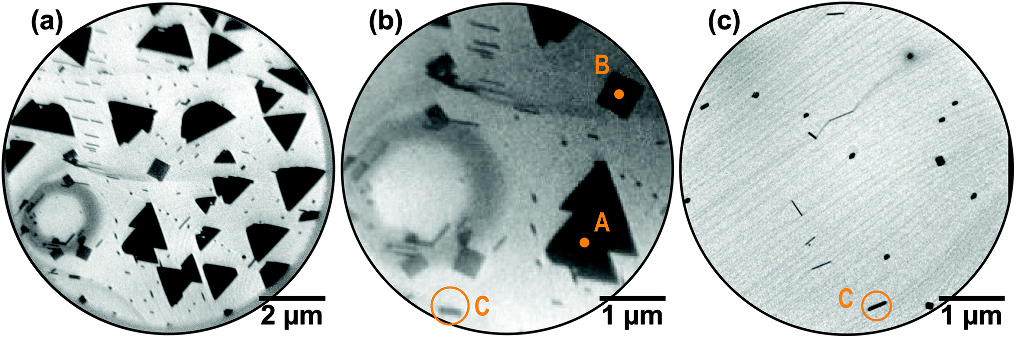 | ||
| Fig. 1 LEEM images of the as-prepared CeO2/Ru(0001) surface after growth at (a and b) 800 °C (electron energy: 28.9 eV) and (c) 1050 °C (electron energy: 22.7 eV). Triangular (“A”), square-like (“B”), and rod-like (“C”) nanostructures are labeled. The dark, round feature in the upper right corner of (c) is a detector artifact. | ||
While the triangular particles clearly constitute the majority surface component at temperatures of about 800 °C, the situation is completely reversed at deposition temperatures above 1000 °C: here, square and rod-like particles are found exclusively (Fig. 1c). Again, atomic steps and step bunches play a dominant role by providing suitable nucleation sites. Interestingly, there are few extremely thin, needle-like objects whose growth direction is found to deviate from the growth direction of their thicker counterparts. This effect is a direct manifestation of the growth process that preferentially proceeds tangentially to the step bunch where the initial nucleation took place. This aspect and its implications will be discussed in further detail in a later section based on the atomic structure of the particles.
AFM was applied ex situ to obtain topographical information on the shape of the particles. A typical micrograph is depicted in Fig. 2a. From the height distribution, mainly two types of objects are identified: large triangular shapes with a height of about 2–3 nm as well as small, tall rectangular and square-like objects exhibiting a height of 5 nm or more. These square-like structures are frequently found to be embedded into CeO2(111) particles as illustrated in the Fig. 2b. This morphology is a direct consequence of the concurrent growth of the ceria(111) majority phase and the rectangular objects, which show a more pronounced three-dimensional growth and hence a much slower lateral growth. From the image, it is obvious that the square-like structure is very rough and may even be composed of smaller building blocks of cubic shape; the triangular particles, to the contrary, are rather flat and smooth in appearance.
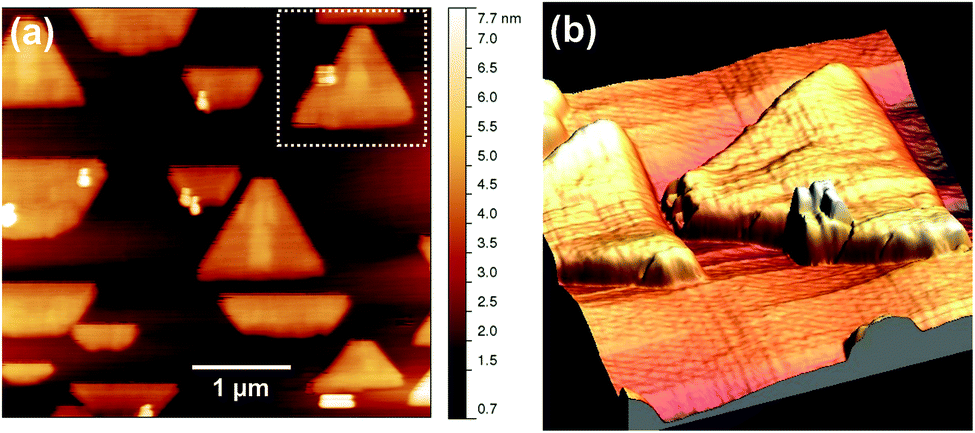 | ||
| Fig. 2 AFM images of the as-prepared CeO2/Ru(0001) surface. (a) Large-scale overview, (b) three-dimensional representation of a CeO2(111) island with an embedded cubic structure recorded in the marked area (dotted line) as shown in (a). | ||
3.2. Oxidation state
The chemical identity of the different ceria particles was confirmed by performing μXAS in XPEEM mode. Fig. 3a displays a PEEM image in which the different particle shapes are simultaneously observed. The photon energy has been tuned to the white line of the Ce M4-edge, resulting in chemical contrast. Since all types of particles are bright, all particles contain cerium. The oxidation state of the individual particles can be analyzed from a collection of PEEM images that have been recorded while the photon energy was tuned through the Ce M4,5 absorption edge. Individual XAS fingerprints for the different particles were extracted by plotting the local intensity of a selected region of interest depending on photon energy (Fig. 3(b)). All spectra show the same spectroscopic signature that is representative of fully oxidized CeO2 particles.36,37 Qualitatively, the increased background intensity for the rectangular islands far off the M4,5 edges indicates a lower work function than what is found for the CeO2(111) surface. Since the rectangular particles are also made of CeO2, this notion therefore suggests a different, probably more open surface orientation of CeO2. Due to the large escape depth of the very slow electrons employed, the different resonance absorption intensities suggest that the rectangular particles are thicker than the triangular particles, compatible with the AFM results.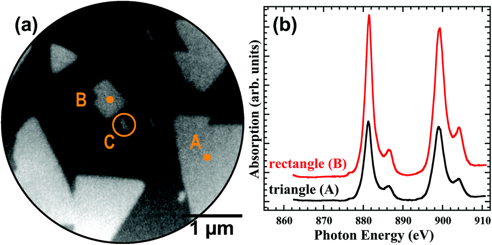 | ||
| Fig. 3 (a) XPEEM image (electron energy: 2.0 eV) of the as-prepared CeO2/Ru(0001) surface recorded at a photon energy (881.5 eV) corresponding to the white line of the Ce M5-edge. (b) Local Ce M-edge X-ray absorption spectra extracted from differently shaped islands. The absorption spectra of the rectangular particles B and C are virtually identical. | ||
3.3. Atomic structure
After establishing that all particles essentially consist of CeO2, we turn to the morphology and crystallographic orientation of the rod-like nanostructures as depicted in Fig. 1c. Using an illumination aperture to confine the incident electron beam to an area of 250 nm in diameter, μLEED patterns have been recorded for the particle labeled “C” in Fig. 1c depending on energy; exemplary patterns are displayed in Fig. 4. Strikingly, all Ru(0001) substrate spots (see Fig. 4a) are elongated in the same direction, evidencing the high step density in this region that fostered the nucleation and growth of the particle. From the comparison of the images, it is evident that the diffraction spots originating from the particle move with energy, which in the LEEM instrument is a clear sign that they originate from inclined surface areas of the particle, i.e., presumably its side facets.38 A false-color cut through three-dimensional reciprocal space from the (−10) to the (10) diffraction spot of Ru(0001) is shown in Fig. 4c. The apparent elongation and splitting of the half-order and integer substrate rods suggests ordering of the substrate steps,39 consistent with the assertion of a high step density. By measuring the tilt angle of the diffraction rods with respect to the surface normal, the inclination of the side facets with respect to the Ru(0001) surface normal is determined to 54.2 ± 0.5°, which is virtually identical to the angle between the [100] and [111] directions in cubic systems (54.74°). Together with the spatial arrangement and symmetry of the facet spots, these results strongly indicate (i) the presence of ceria(111) side facets, (ii) that the top facets are very small or even non-existing, and (iii) that the crest of the pyramidal-shaped ceria nanorods is orthogonal to the ceria [100] direction. This finding is essentially in accordance with the results by Fronzi and coworkers based on DFT calculations that, under oxygen-lean conditions, favored a truncated octahedral ceria particle shape with {111} side facets and a small {100} top facet.40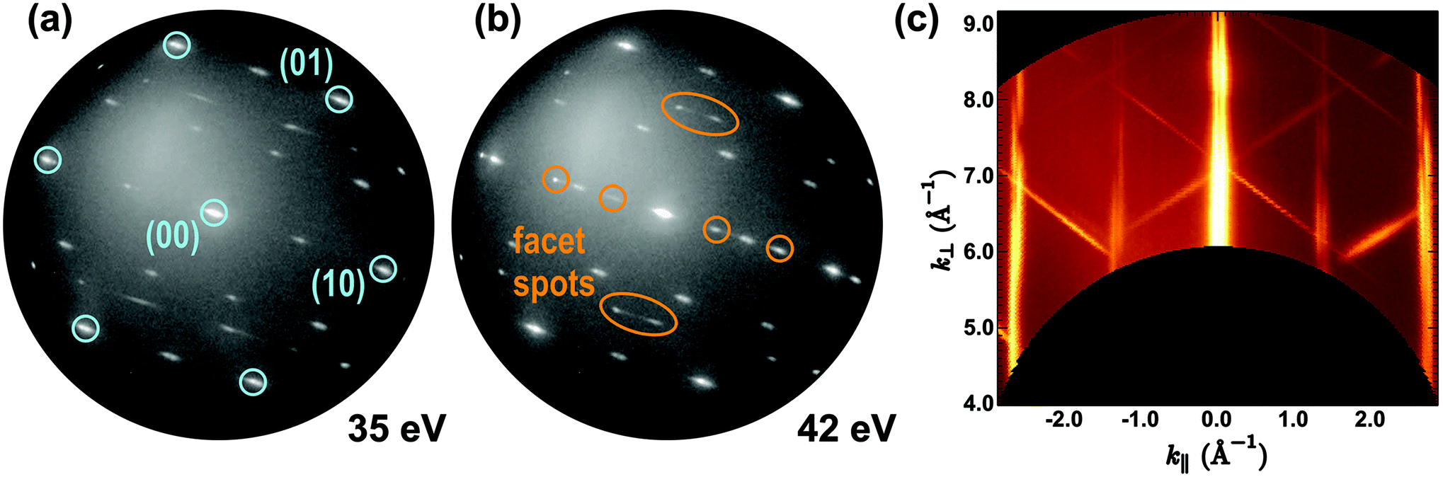 | ||
| Fig. 4 (a and b) μLEED patterns acquired of the square island labeled “C” of the as-prepared CeO2/Ru(0001) surface displayed in Fig. 1(c). The surrounding p(2 × 2) hexagonal spots are due to the oxygen adlayer of the Ru(0001) surface. (c) Reciprocal space map revealing the side facet orientations of the ceria nanorods. Non-vertical surface lattice rods indicate tilted ceria facets and allow determining their inclination angle. | ||
The presence of a flat, ordered top facet for square-like ceria nanostructures is clearly demonstrated by the μLEED pattern recorded from the particle “B” (Fig. 1b) as shown in Fig. 5a. Besides the hexagonal Ru(0001) diffraction spots, originating from the co-illuminated Ru(0001) surface at the sides of the island, also weaker peaks with fourfold symmetry are observed. Their lateral arrangement is compatible with the integer reflections of the (1 × 1)-periodic CeO2(001) surface as illustrated by the schematic LEED pattern displayed in Fig. 5b, in which an in-plane ceria lattice constant of 3.826 Å has been assumed. Contrary to Fig. 4, no facet spots were observed. Therefore, this diffraction pattern evidences the growth of CeO2(001) nanocrystals with (1 × 1) periodicity. In the following, we will investigate the two major conclusions that follow from this finding, i.e., (i) the relative azimuthal orientation of the particle and substrate lattices, and (ii) the apparent absence of a surface reconstruction of the ceria(001) top facet.
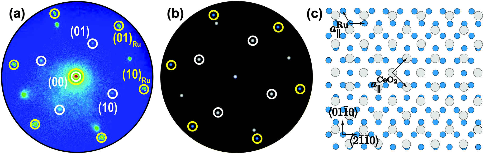 | ||
| Fig. 5 (a) μLEED pattern (40 eV) acquired of the square island labeled “B” of the as-prepared CeO2/Ru(0001) surface displayed in Fig. 1(b). The Ru and ceria spots are marked by yellow and white circles, respectively. The Ru spots are the contribution from the surrounding Ru(0001) surface that was also illuminated despite the use of the 500 μm aperture. (b) Schematic LEED pattern assuming a hexagonal Ru lattice (2.706 Å) and a square ceria lattice (3.826 Å). (c) Real-space coincidence lattice deduced from the observed azimuthal alignment (a) of the Ru and ceria lattices. | ||
Real-space modeling of the lateral atomic arrangement that is compatible with the μLEED pattern (Fig. 5a) reveals the formation of a coincidence lattice at the metal–oxide interface as depicted in Fig. 5c: the CeO2 bulk lattice constant ( ) matches two times the nearest-neighbor distance of Ru(0001) (aRu∥ = 2.706 Å), resulting in a virtually unstrained coincidence arrangement in one of the symmetrically equivalent 〈2
![[1 with combining macron]](https://www.rsc.org/images/entities/char_0031_0304.gif) 0〉 directions of the substrate. In the perpendicular 〈010〉 directions, the ceria bulk lattice constant and the substrate row spacing (
0〉 directions of the substrate. In the perpendicular 〈010〉 directions, the ceria bulk lattice constant and the substrate row spacing (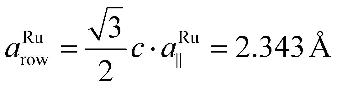 ) have to be considered. Assuming perfect lattice matching for the double nearest-neighbor distance and the ceria bulk lattice (
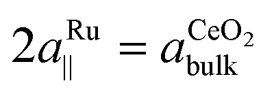 ), a ratio of
 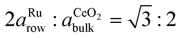 is obtained, which can be approximated by 13
![[thin space (1/6-em)]](https://www.rsc.org/images/entities/char_2009.gif) :15 with an error less than 10−4. Therefore, perfect matching is reached when 13 ceria bulk lattice constants match 30 times the substrate row spacing, which may be described by a superstructure in matrix notation:
:15 with an error less than 10−4. Therefore, perfect matching is reached when 13 ceria bulk lattice constants match 30 times the substrate row spacing, which may be described by a superstructure in matrix notation: 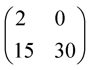 . However, as the ceria nanocrystals are several nanometers thick, the presence of such a coincidence bonding geometry between the ceria and the substrate cannot be verified by LEED. Nonetheless, especially the excellent match in the 〈20〉 directions provides an intuitive explanation for the observation of preferred azimuthal orientations of the nanostructures, implying that such an atomic bonding geometry is thermodynamically favorable and hence, in addition to the direction of the step edges, one of the decisive factors for the orientation of the crystallographic axes of the particles during the initial nucleation and growth process.
We have used STM to probe also in real space the morphology and atomic structure of isolated, comparatively large square and rod-like particles. A representative survey image taken after ceria growth at 700 °C is reproduced in Fig. 6a. Clearly, large and flat triangular ceria(111) islands are seen to coexist with many smaller, rectangular nanostructures, consistent with our previous findings from LEEM (Fig. 1) and AFM (Fig. 2). However, after growth at 830 °C also much larger rectangular patches are visible (Fig. 6b) whose top facets are large and smooth enough to allow for investigating their crystallographic structure and surface termination. A high-resolution image of the region indicated by a solid rectangle in Fig. 6b is represented in Fig. 6c. Clearly, a p(2 × 2) reconstruction is resolved that spans the whole imaged region. Before we rationalize why this p(2 × 2) reconstruction does not show up in μLEED (see Fig. 5), we discuss further structural details. Analysis of the line profile also reveals a single atomic step between the lower terrace (left part) and the upper terrace (center to right part) of the ceria(001) island. The typical corrugation amounts to about 0.3 Å, but occasionally deeper pits are discerned that, based on the imaging conditions, are attributed to statistically distributed point defects.
 | ||
| Fig. 6 STM empty-state, constant-current images displaying the morphology and atomic structure of the as-prepared CeO2/Ru(0001) surface. (a) Overview (differentiated image, sample bias 2.5 V, tunneling current 0.2 nA) showing small square and rectangular ceria particles coexisting with large triangular particles after growth at 700 °C. (b) For growth at 830 °C and higher ceria coverages, also larger rectangular particles can be found, mostly near significant step bunches and defects (differentiated image, sample bias 2.0 V, tunneling current 0.2 nA). (c) High-resolution image (sample bias 3.0 V, tunneling current 0.3 nA) acquired on the top facet of the large rectangular particle as indicated in (b). The lower and upper terraces exhibit a p(2 × 2) reconstruction and are separated by a single step. | ||
The finding of a p(2 × 2) reconstruction is in agreement with the STM data from Pan et al. who identified two types of surface reconstructions, i.e., a c(2 × 2) and a p(2 × 2) surface periodicity, after annealing to temperatures of about 530 to 830 °C.28 On the basis of density functional theory (DFT) calculations, these surface reconstructions have been traced back to two different surface terminations, an O termination (“Bn-type structure”) for the c(2 × 2) and a Ce termination (“Cn-type structure”) for the p(2 × 2) surface. From thermodynamical considerations, the Cn structures, i.e., the p(2 × 2) structures, were found to be most stable, consistent with our findings for growth at high temperatures. Furthermore, the results of the DFT calculations suggested that under UHV conditions a considerable amount of O vacancies should be present, whose density could also possibly be further increased because of electron irradiation. If these defects are incorporated in a manner such that anti-phase domain boundaries are formed, the (2 × 2) superstructure spots will be weakened considerably or even disappear completely, yielding a (1 × 1) LEED pattern, consistent with our observations (Fig. 5a).
3.4. Crystallographic particle shape
Based on STM and LEED, we may propose a model for the particle shape of the large rectangular particles and the oxide nanorods. The observation of the (001) top facet reconstruction of the large rectangular particle by STM (Fig. 6c) and the identification of the in-plane [110] and [10] directions enable the labeling of the crystallographic directions perpendicular to the particle edges. The result of this procedure is marked in the STM image (Fig. 6b): the long, straight edges of the particle are found to be oriented perpendicular to the <100> directions whereas the corners are delimited by shorter edges perpendicular to the <110> directions. Independent determination of the substrate orientation by STM reveals a parallel alignment of the oxide [010] and the substrate [![[2 with combining macron]](https://www.rsc.org/images/entities/char_0032_0304.gif) 110] direction, consistent with the LEED observation and the inferred condition for the coincidence lattice (Fig. 5). Taken together, these findings suggest that the large rectangular nanocrystals are either of truncated octahedral shape28,40 or, more likely since we have never observed reflections from side facets in μLEED, of cuboidal (“brick-like”) shape, similar to wet-chemically prepared ceria nanocubes.41
110] direction, consistent with the LEED observation and the inferred condition for the coincidence lattice (Fig. 5). Taken together, these findings suggest that the large rectangular nanocrystals are either of truncated octahedral shape28,40 or, more likely since we have never observed reflections from side facets in μLEED, of cuboidal (“brick-like”) shape, similar to wet-chemically prepared ceria nanocubes.41
3.5. Growth of CeO2(111) vs. CeO2(001) particles
Lastly, we discuss the physical origin for the formation of the (001) orientation as compared to the conventionally observed (111) orientation. In the case of Cu(111) it has been suggested that the formation of an interfacial copper oxide may stabilize the growth of ceria(001).18 However, at the growth conditions employed here the formation of ruthenium oxide species, which using intensity–voltage LEEM can clearly be distinguished and identified on the few nanometer scale,42 has not been observed. From our XAS data that corroborated an identical oxidation state close to Ce4+ for the coexisting ceria particles, it is obvious that the transition from CeO2 to Ce2O3 is not the driving force for ceria(001) formation, as has previously been argued on the basis of thermodynamical considerations and predictions by the Gibbs–Wulff theorem.28 Instead, the difference in the Gibbs free energies of the different surface orientations must be counterbalanced by an additional term that essentially inverts the stability considerations purely based on the individual surface free energies. Based on the presence of a coincidence lattice between the ceria(001) particles and the Ru(0001) as identified by μLEED, we hence infer that this additional term in the total Gibbs free energy is given by the interfacial energy between the particle and the substrate and that it is large enough to compensate for the slightly less favorable energetics of the ceria(001) surface. Also, in view of our LEEM results we propose that the coincidence lattice plays a dominant role for their stabilization at high temperatures. This statement may in fact be interpreted as a generalization of the behavior of the differently oriented ceria(111) domains at high temperatures of about 900 °C, where we had already noticed the absence of ceria(111) rotational domains whose principal axes are azimuthally rotated with respect to the 〈20〉 main symmetry directions of the Ru(0001) substrate.17 However, to arrive at a fully coherent picture of the nucleation and growth process of ceria on ruthenium, especially at lower temperatures, additional kinetic factors, which are beyond the scope of the present investigation, need to be considered to explain the preferential occurrence of the (111) versus the (001) orientation.
4. Conclusion
We have identified the formation of ceria(001) islands at near-UHV growth conditions. These islands are easily recognized by their square (cuboidal) or rod-like (truncated octahedral) shape, and they coexist with the ceria(111) majority phase over a wide range of temperatures. The ceria(001) particles are predominantly found at step bunches of the ruthenium(0001) substrate, and they may exclusively be grown at very high temperatures in excess of 1000 °C. The origin of their stability has been traced back to the existence of a coincidence lattice formed at the oxide–substrate interface that reverts the considerations based purely on the Gibbs surface free energies of the different ceria orientations. These results should prove crucial in understanding the complex cerium oxide epitaxy on late transition metals and, by enabling selective preparation of well-defined ceria nanostructures of specific orientation in well-defined environments, pave the road toward in-depth studies of structure–activity relations in model heterogeneous catalysis.Acknowledgements
Technical support by Percy Zahl, Peter Sutter (Center for Functional Nanomaterials, BNL), and Gary Nintzel (NSLS, BNL) as well as Jürgen Lauckner and Torben Rohbeck (University of Bremen) is gratefully acknowledged. This research used resources of the Center for Functional Nanomaterials and National Synchrotron Light Source, which are U.S. DOE Office of Science User Facilities, at Brookhaven National Laboratory under Contract no. DE-SC0012704. The research leading to these results has received funding from the European Community's Seventh Framework Programme (FP7/2007-2013) under grant agreement no. 312284. S. G. thanks the German Academic Exchange Service for funding a research stay at the University of Bremen as part of a DAAD fellowship 2014 for university academics. Also, support by the EU COST Action CM1104 is acknowledged. Finally, we thank Thomas Schmidt (University of Bremen) for stimulating discussions.References
- J. A. Rodriguez, S. Ma, P. Liu, J. Hrbek, J. Evans and M. Pérez, Science, 2007, 318, 1757–1760 CrossRef CAS PubMed.
- S. Surnev, A. Fortunelli and F. P. Netzer, Chem. Rev., 2013, 113, 4314–4372 CrossRef CAS PubMed.
- A. Trovarelli, Catal. Rev., 1996, 38, 439–520 CAS.
- H. Nörenberg and J. Harding, Surf. Sci., 2001, 477, 17–24 CrossRef.
- Z. Wu, M. Li, D. R. Mullins and S. H. Overbury, ACS Catal., 2012, 2, 2224–2234 CrossRef CAS.
- D. R. Mullins, Surf. Sci. Rep., 2015, 70, 42–85 CrossRef CAS.
- M. Alexandrou and R. M. Nix, Surf. Sci., 1994, 321, 47–57 CrossRef CAS.
- C. Hardacre, G. M. Roe and R. M. Lambert, Surf. Sci., 1995, 326, 1–10 CrossRef CAS.
- K.-D. Schierbaum, Surf. Sci., 1998, 399, 29–38 CrossRef CAS.
- D. R. Mullins, P. V. Radulovic and S. H. Overbury, Surf. Sci., 1999, 429, 186–198 CrossRef CAS.
- S. Eck, C. Castellarin-Cudia, S. Surnev, M. G. Ramsey and F. P. Netzer, Surf. Sci., 2002, 520, 173–185 CrossRef CAS.
- J.-L. Lu, H.-J. Gao, S. Shaikhutdinov and H.-J. Freund, Surf. Sci., 2006, 600, 5004–5010 CrossRef CAS.
- V. Matolín, L. Libra, I. Matolínová, V. Nehasil, L. Sedláček and F. Šutara, Appl. Surf. Sci., 2007, 254, 153–155 CrossRef.
- S. Ma, J. Rodriguez and J. Hrbek, Surf. Sci., 2008, 602, 3272–3278 CrossRef CAS.
- D. C. Grinter, R. Ithnin, C. L. Pang and G. Thornton, J. Phys. Chem. C, 2010, 114, 17036–17041 CAS.
- P. Luches, F. Pagliuca and S. Valeri, J. Phys. Chem. C, 2011, 115, 10718–10726 CAS.
- B. Kaemena, S. D. Senanayake, A. Meyer, J. T. Sadowski, J. Falta and J. I. Flege, J. Phys. Chem. C, 2013, 117, 221–232 CAS.
- F. Yang, Y. Choi, S. Agnoli, P. Liu, D. Stacchiola, J. Hrbek and J. A. Rodriguez, J. Phys. Chem. C, 2011, 115, 23062–23066 CAS.
- O. Stetsovych, J. Beran, F. Dvořák, K. Mašek, J. Mysliveček and V. Matolín, Appl. Surf. Sci., 2013, 285(Part B), 766–771 CrossRef CAS.
- J. Höcker, T. Duchoň, K. Veltruská, V. Matolín, J. Falta, S. D. Senanayake and J. I. Flege, J. Chem. Phys. C, 2016, 120, 4895–4901 CrossRef.
- G. Vilé, S. Colussi, F. Krumeich, A. Trovarelli and J. Pérez-Ramírez, Angew. Chem., Int. Ed., 2014, 53, 12069–12072 CrossRef PubMed.
- J. Höcker, T. O. Menteş, A. Sala, A. Locatelli, T. Schmidt, J. Falta, S. D. Senanayake and J. I. Flege, Adv. Mater. Interfaces, 2015, 2, 1500314 Search PubMed.
- T. Inoue, T. Ohsuna, L. Luo, X. D. Wu, C. J. Maggiore, Y. Yamamoto, Y. Sakurai and J. H. Chang, Appl. Phys. Lett., 1991, 59, 3604 CrossRef CAS.
- T. Ami, Y. Ishida, N. Nagasawa, A. Machida and M. Suzuki, Appl. Phys. Lett., 2001, 78, 1361 CrossRef CAS.
- V. F. Solovyov, K. Develos-Bagarinao and D. Nykypanchuk, Phys. Rev. B: Condens. Matter, 2009, 80, 104102 CrossRef.
- V. F. Solovyov, T. Ozaki, A. Atrei, L. Wu, A. Al-Mahboob, J. T. Sadowski, X. Tong, D. Nykypanchuk and Q. Li, Sci. Rep., 2014, 4, 4627 Search PubMed.
- J. I. Flege, B. Kaemena, S. D. Senanayake, J. Höcker, J. T. Sadowski and J. Falta, Ultramicroscopy, 2013, 130, 87–93 CrossRef CAS PubMed.
- Y. Pan, N. Nilius, C. Stiehler, H.-J. Freund, J. Goniakowski and C. Noguera, Adv. Mater. Interfaces, 2014, 1, 1400404 Search PubMed.
- T. E. Madey, H. A. Engelhardt and D. Menzel, Surf. Sci., 1975, 48, 304–328 CrossRef CAS.
- J. I. Flege, J. Hrbek and P. Sutter, Phys. Rev. B: Condens. Matter, 2008, 78, 165407 CrossRef.
- A. Locatelli, L. Aballe, T. O. Menteş, M. Kiskinova and E. Bauer, Surf. Interface Anal., 2006, 38, 1554–1557 CrossRef CAS.
- J. I. Flege, E. Vescovo, G. Nintzel, L. H. Lewis, S. Hulbert and P. Sutter, Nucl. Instrum. Methods Phys. Res., Sect. B, 2007, 261, 855–858 CrossRef CAS.
- A. Locatelli and E. Bauer, J. Phys.: Condens. Matter, 2008, 20, 093002 CrossRef.
- P. Zahl, T. Wagner, R. Möller and A. Klust, J. Vac. Sci. Technol., B, 2010, 28, C4E39–C4E47 CAS.
- J. I. Flege and E. E. Krasovskii, Phys. Status Solidi RRL, 2014, 8, 463–477 CrossRef CAS.
- C. Dong, A. Augustsson, C. Chen, C. Chang, Y. Chen and J.-H. Guo, J. Electron Spectrosc. Relat. Phenom., 2005, 144–147, 581–584 CrossRef CAS.
- S. Alayoglu, K. An, G. Melaet, S. Chen, F. Bernardi, L. W. Wang, A. E. Lindeman, N. Musselwhite, J. Guo, Z. Liu, M. A. Marcus and G. A. Somorjai, J. Phys. Chem. C, 2013, 117, 26608–26616 CAS.
- J. Wollschläger, J. Falta and M. Henzler, Appl. Phys. A, 1990, 50, 57–68 CrossRef.
- J. Falta, R. Imbihl, M. Sander and M. Henzler, Phys. Rev. B: Condens. Matter, 1992, 45, 6858–6867 CrossRef CAS.
- M. Fronzi, A. Soon, B. Delley, E. Traversa and C. Stampfl, J. Chem. Phys., 2009, 131, 104701 CrossRef.
- S. Yang and L. Gao, J. Am. Chem. Soc., 2006, 128, 9330–9331 CrossRef CAS PubMed.
- J. I. Flege, B. Herd, J. C. Goritzka, H. Over, E. E. Krasovskii and J. Falta, ACS Nano, 2015, 9, 8468–8473 CrossRef CAS PubMed.
| This journal is © The Royal Society of Chemistry 2016 |